Arduino FreeRTOS

Arduino FreeRTOS Logo

For a long time I have been using the AVR port of FreeRTOS as the platform for my Arduino hardware habit. I’ve written (acquired, stolen, and corrupted) a plethora of different drivers and solutions for the various projects I’ve built over the last years. But, sometimes it would be nice to just try out a new piece of hardware in a solid multi-tasking environment without having to dive into the datasheets and write code. Also, when time is of the essence rewriting someone’s existing driver is just asking for stress and failure.

So recently, with an important hack-a-thon coming up, I thought it would be nice to build a robust FreeRTOS implementation that can just shim into the Arduino IDE and allow me to use the best parts of both environments, seamlessly.

Arduino IDE Core is just AVR

One of the good things about the Arduino core environment is that it is just the normal AVR environment with a simple Java IDE added. That means that all of the AVR command line tools used to build Arduino sketches will also just work my AVR port of FreeRTOS.

Some key aspects of the AVR FreeRTOS port have been adjusted to create the seamless integration with the Arduino IDE. These optimizations are not necessarily the best use of FreeRTOS, but they make the integration much easier.

FreeRTOS needs to have an interrupt timer to trigger the scheduler to check which task should be using the CPU, and to fairly distribute processing time among equivalent priority tasks. In the case of the Arduino environment all of the normal timers are configured in advance, and therefore are not available for use as the system_tick timer. However, all AVR ATmega devices have a watchdog timer which is driven by an independent 128kHz internal oscillator. Arduino doesn’t configure the watchdog timer, and conveniently the watchdog configuration is identical across the entire ATmega range. That means that the entire range of classic AVR based Arduino boards can be supported within FreeRTOS with one system_tick configuration.

The Arduino environment has only two entry point functions available for the user, setup() and loop(). These functions are written into an .ino file and are linked together with and into a main() function present in the Arduino libraries. The presence of a fixed main() function within the Arduino libraries makes it really easy to shim FreeRTOS into the environment.

The main() function in the main.c file contains a initVariant() weak attribute stub function prior to the internal Arduino initialisation setup() function. By implementing an initVariant() function execution can be diverted into the FreeRTOS environment, after calling the normal setup() initialisation, by simply continuing to start the FreeRTOS scheduler.

int main(void) // Normal Arduino main.cpp. Normal execution order.
{
init();
initVariant(); // Our initVariant() diverts execution from here.
setup(); // The Arduino setup() function.

for (;;)
{
loop(); // The Arduino loop() function.
if (serialEventRun) serialEventRun();
}
return 0;
}

Firstly, this initVariant() function is located in the variantHooks.cpp file in the FreeRTOS library. It replaces the weak attribute function definition in the Arduino core.

void initVariant(void)
{
setup(); // The Arduino setup() function.
vTaskStartScheduler(); // Initialise and run the FreeRTOS scheduler. Execution should never return to here.
}

Secondly, the FreeRTOS idle task is used to run the loop() function whenever there is no unblocked FreeRTOS task available to run. In the trivial case, where there are no configured FreeRTOS tasks, the loop() function will be run exactly as normal, with the exception that a short scheduler interrupt will occur every 15 milli-seconds (configurable). This function is located in the variantHooks.cpp file in the library.

void vApplicationIdleHook( void )
{
loop(); // The Arduino loop() function.
if (serialEventRun) serialEventRun();
}

Putting these small changes into the Arduino IDE, together with a single directory containing the necessary FreeRTOS v10.x.x files configured for AVR, is all that needs to be done to slide the FreeRTOS shim under the Arduino environment.

I have published the relevant files on Github where the commits can be browsed and the repository downloaded. The simpler solution is to install FreeRTOS using the Arduino Library Manager, or download the ZIP files from Github and install manually as a library in your Arduino IDE.

Getting Started with FreeRTOS

Ok, with these simple additions to the Arduino IDE via a normal Arduino library, we can get started.

Firstly in the Arduino IDE Library manager, from Version 1.6.8, look for the FreeRTOS library under the Type: “Contributed” and the Topic: “Timing”.

Arduino Library Manager

Arduino Library Manager

Ensure that the most recent FreeRTOS library is installed. As of writing that is v10.3.0-4.

FreeRTOS v8.2.3-6 Installed

Example of FreeRTOS v8.2.3-6 Installed

Then under the Sketch->Include Library menu, ensure that the FreeRTOS library is included in your sketch. A new empty sketch will look like this.

ArduinoIDE_FreeRTOS

Compile and upload this empty sketch. This will show you how much of your flash is consumed by the FreeRTOS scheduler. As a guide the following information was compiled using Arduino v1.8.5 on Windows 10.

// Device: loop() -> FreeRTOS | Additional Program Storage
// Uno: 444 -> 6592 | 20%
// Goldilocks: 502 -> 6684 | 5%
// Leonardo: 3462 -> 9586 | 23%
// Yun: 3456 -> 9580 | 23%
// Mega: 662 -> 6898 | 2%

Now test and upload the Blink sketch, with an underlying Real-Time Operating System. That’s all there is to having FreeRTOS running in your sketches. So simple.

Next Steps

Blink_AnalogRead.ino is a good way to take the next step as it combines two basic Arduino examples, Blink and AnalogRead into one sketch with in two separate tasks. Both tasks perform their duties, managed by the FreeRTOS scheduler.

#include

// define two tasks for Blink and AnalogRead
void TaskBlink( void *pvParameters );
void TaskAnalogRead( void *pvParameters );

// the setup function runs once when you press reset or power the board
void setup()
{
// Now set up two tasks to run independently.
xTaskCreate(
TaskBlink
, "Blink"; // A name just for humans
, 128      // This stack size can be checked and adjusted by reading the Stack Highwater
, NULL
, 2        // Priority, with 3 (configMAX_PRIORITIES - 1) being the highest, and 0 being the lowest.
, NULL );

xTaskCreate(
TaskAnalogRead
, "AnalogRead";
, 128      // Stack size
, NULL
, 1        // Priority, with 3 (configMAX_PRIORITIES - 1) being the highest, and 0 being the lowest.
, NULL );

// Now the task scheduler, which takes over control of scheduling individual tasks, is automatically started.
}

void loop()
{
// Empty. Things are done in Tasks. Never Block or delay.
}

/*--------------------------------------------------*/
/*---------------------- Tasks ---------------------*/
/*--------------------------------------------------*/

void TaskBlink(void *pvParameters) // This is a task.
{
(void) pvParameters;

// initialize digital pin 13 as an output.
pinMode(13, OUTPUT);

for (;;) // A Task shall never return or exit.
{
digitalWrite(13, HIGH); // turn the LED on (HIGH is the voltage level)
vTaskDelay( 1000 / portTICK_PERIOD_MS ); // wait for one second
digitalWrite(13, LOW); // turn the LED off by making the voltage LOW
vTaskDelay( 1000 / portTICK_PERIOD_MS ); // wait for one second
}
}

void TaskAnalogRead(void *pvParameters) // This is a task.
{
(void) pvParameters;

// initialize serial communication at 9600 bits per second:
Serial.begin(9600);

for (;;)
{
// read the input on analog pin 0:
int sensorValue = analogRead(A0);
// print out the value you read:
Serial.println(sensorValue);
vTaskDelay(1); // one tick delay (15ms) in between reads for stability
}
}

Next there are a number of examples in the FreeRTOS Quick Start Guide.

One last important thing you can do is to reduce device power consumption by not using the default loop() function for anything more than putting the MCU to sleep. This code below can be used for simply putting the MCU into a sleep mode of your choice, while no tasks are unblocked. Remember that the loop() function shouldn’t ever disable interrupts and block processing.

#include // include the Arduino (AVR) sleep functions.

loop() // Remember that loop() is simply the FreeRTOS idle task. Something to do, when there's nothing else to do.
{
// Digital Input Disable on Analogue Pins
// When this bit is written logic one, the digital input buffer on the corresponding ADC pin is disabled.
// The corresponding PIN Register bit will always read as zero when this bit is set. When an
// analogue signal is applied to the ADC7..0 pin and the digital input from this pin is not needed, this
// bit should be written logic one to reduce power consumption in the digital input buffer.

#if defined(__AVR_ATmega640__) || defined(__AVR_ATmega1280__) || defined(__AVR_ATmega1281__) || defined(__AVR_ATmega2560__) || defined(__AVR_ATmega2561__) // Mega with 2560
DIDR0 = 0xFF;
DIDR2 = 0xFF;
#elif defined(__AVR_ATmega644P__) || defined(__AVR_ATmega644PA__) || defined(__AVR_ATmega1284P__) || defined(__AVR_ATmega1284PA__) // Goldilocks with 1284p
DIDR0 = 0xFF;

#elif defined(__AVR_ATmega328P__) || defined(__AVR_ATmega168__) || defined(__AVR_ATmega8__) // assume we're using an Arduino with 328p
DIDR0 = 0x3F;

#elif defined(__AVR_ATmega32U4__) || defined(__AVR_ATmega16U4__) // assume we're using an Arduino Leonardo with 32u4
DIDR0 = 0xF3;
DIDR2 = 0x3F;
#endif

// Analogue Comparator Disable
// When the ACD bit is written logic one, the power to the Analogue Comparator is switched off.
// This bit can be set at any time to turn off the Analogue Comparator.
// This will reduce power consumption in Active and Idle mode.
// When changing the ACD bit, the Analogue Comparator Interrupt must be disabled by clearing the ACIE bit in ACSR.
// Otherwise an interrupt can occur when the ACD bit is changed.
ACSR &= ~_BV(ACIE);
ACSR |= _BV(ACD);

// There are several macros provided in the header file to actually put
// the device into sleep mode.
// SLEEP_MODE_IDLE (0)
// SLEEP_MODE_ADC (_BV(SM0))
// SLEEP_MODE_PWR_DOWN (_BV(SM1))
// SLEEP_MODE_PWR_SAVE (_BV(SM0) | _BV(SM1))
// SLEEP_MODE_STANDBY (_BV(SM1) | _BV(SM2))
// SLEEP_MODE_EXT_STANDBY (_BV(SM0) | _BV(SM1) | _BV(SM2))

set_sleep_mode( SLEEP_MODE_IDLE );

portENTER_CRITICAL();
sleep_enable();

// Only if there is support to disable the brown-out detection.
#if defined(BODS) && defined(BODSE)
sleep_bod_disable();
#endif

portEXIT_CRITICAL();
sleep_cpu(); // good night.

// Ugh. I've been woken up. Better disable sleep mode.
sleep_reset(); // sleep_reset is faster than sleep_disable() because it clears all sleep_mode() bits.
}

o that’s all there is to it. There’s nothing more to do except to read the FreeRTOS Quick Start Guide.
Further reading with manicbug, and by searching on this site too.

General Usage

FreeRTOS has a multitude of configuration options, which can be specified from within the FreeRTOSConfig.h file. To keep commonality with all of the Arduino hardware options, some sensible defaults have been selected.

The AVR Watchdog Timer is used with to generate 15ms time slices, but Tasks that finish before their allocated time will hand execution back to the Scheduler. This does not affect the use of any of the normal Timer functions in Arduino.

Time slices can be selected from 15ms up to 500ms. Slower time slicing can allow the Arduino MCU to sleep for longer, without the complexity of a Tickless idle.

Watchdog period options:

  • WDTO_15MS
  • WDTO_30MS
  • WDTO_60MS
  • WDTO_120MS
  • WDTO_250MS
  • WDTO_500MS

Note that Timer resolution is affected by integer math division and the time slice selected. Trying to accurately measure 100ms, using a 60ms time slice for example, won’t work.

Stack for the loop() function has been set at 192 bytes. This can be configured by adjusting the configIDLE_STACK_SIZE parameter. It should not be less than the configMINIMAL_STACK_SIZE. If you have stack overflow issues, just increase it. Users should prefer to allocate larger structures, arrays, or buffers using pvPortMalloc(), rather than defining them locally on the stack. Or, just declare them as global variables.

Memory for the heap is allocated by the normal malloc() function, wrapped by pvPortMalloc(). This option has been selected because it is automatically adjusted to use the capabilities of each device. Other heap allocation schemes are supported by FreeRTOS, and they can used with additional configuration.

Never use the Arduino delay() function in your Tasks, as it burns CPU cycles and doesn’t place the Task into Blocked State, allowing the Scheduler to place other lower priority tasks into Running State. Use vTaskDelay() or vTaskDelayUntil() instead. Also never delay or Block the Arduino loop() as this is being run by the FreeRTOS Idle Task, which must never be blocked.

Errors

  • Stack Overflow: If any stack (for the loop() or) for any Task overflows, there will be a slow LED blink, with 4 second cycle.
  • Heap Overflow: If any Task tries to allocate memory and that allocation fails, there will be a fast LED blink, with 100 millisecond cycle.

Compatibility

  • ATmega328 @ 16MHz : Arduino UNO, Arduino Duemilanove, Arduino Diecimila, etc.
  • ATmega328 @ 16MHz : Adafruit Pro Trinket 5V, Adafruit Metro 328, Adafruit Metro Mini
  • ATmega328 @ 16MHz : Seeed Studio Stalker
  • ATmega328 @ 16MHz : Freetronics Eleven, Freetronics 2010
  • ATmega328 @ 12MHz : Adafruit Pro Trinket 3V
  • ATmega32u4 @ 16MHz : Arduino Leonardo, Arduino Micro, Arduino Yun, Teensy 2.0
  • ATmega32u4 @ 8MHz : Adafruit Flora, Bluefruit Micro
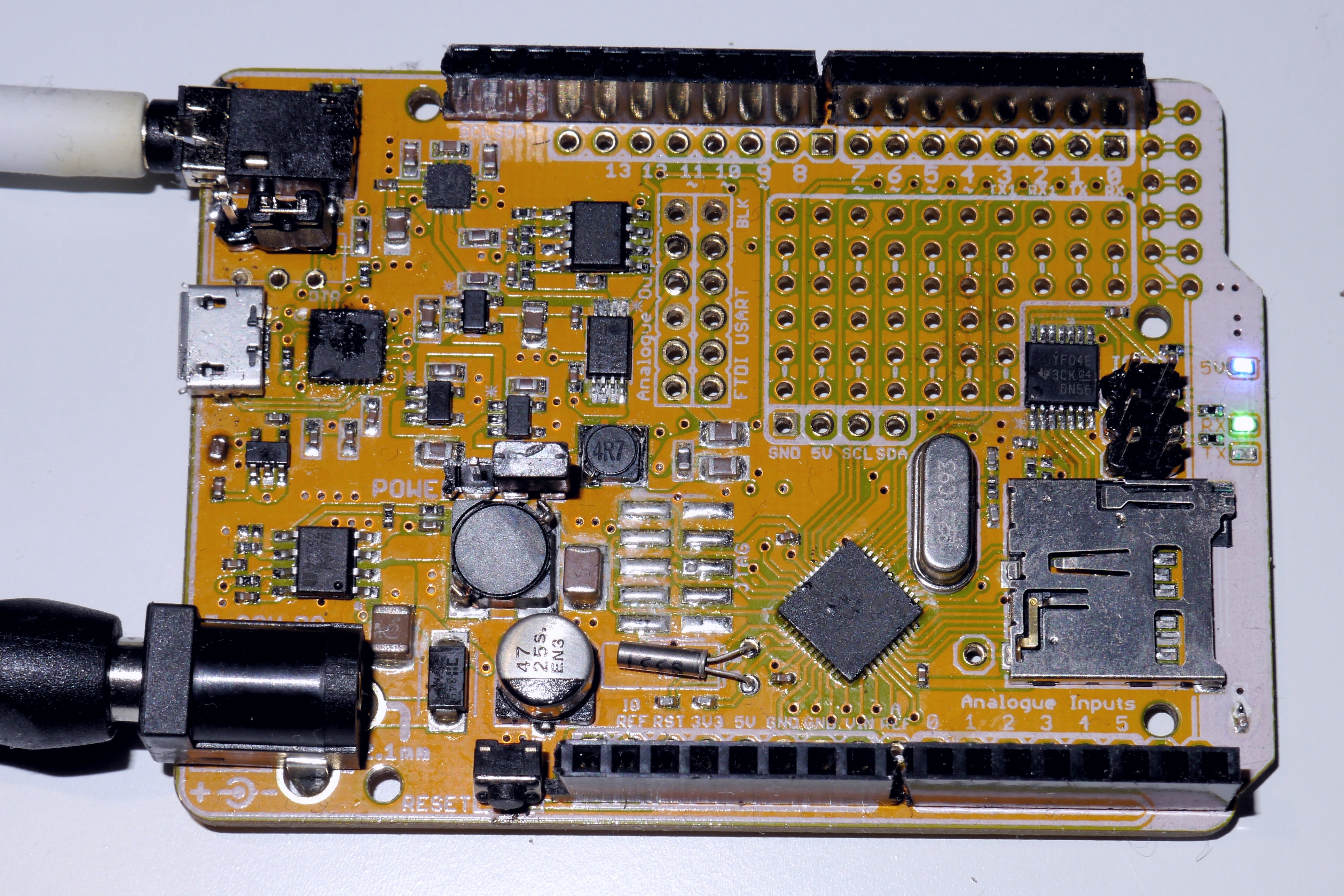
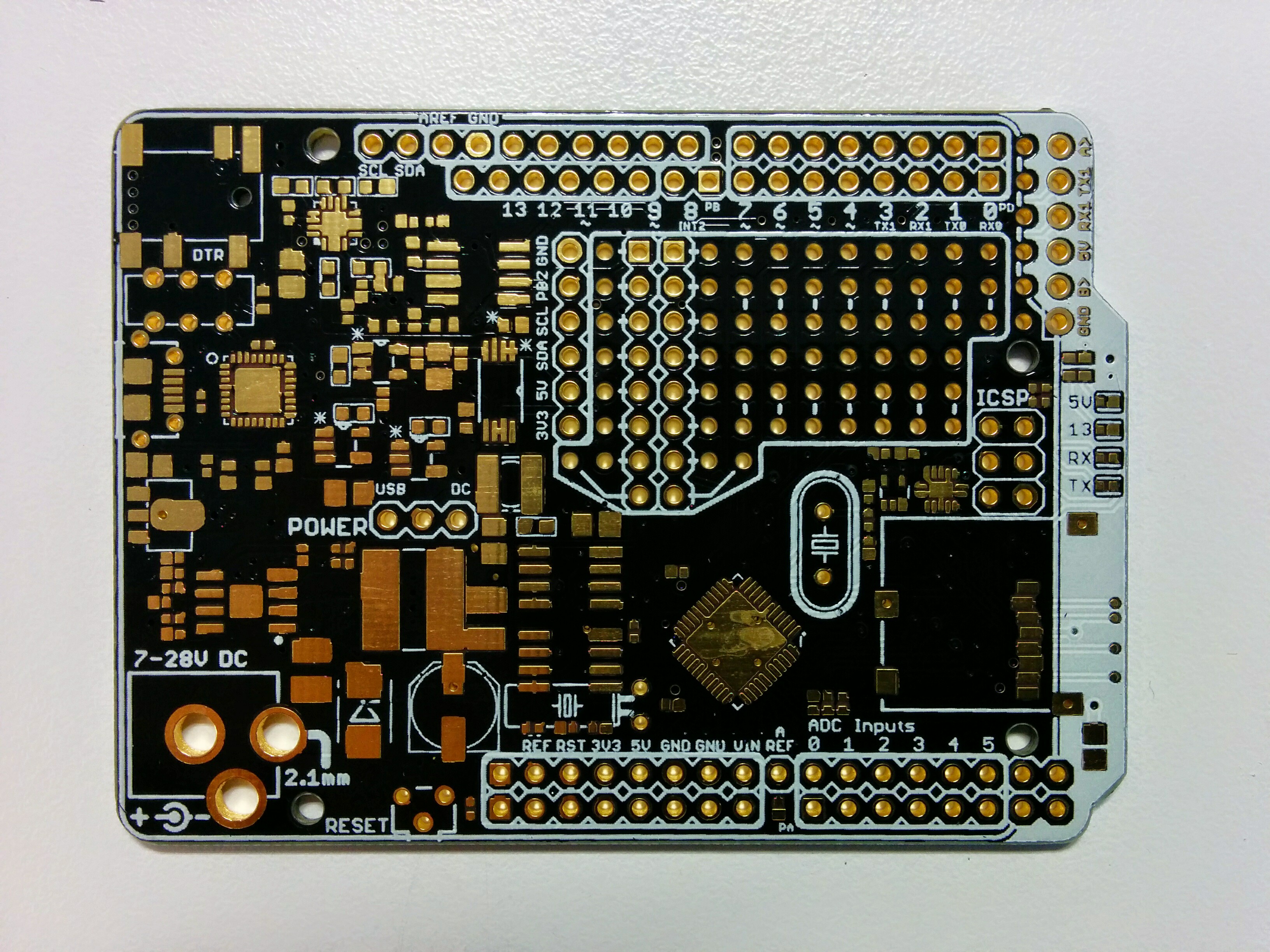
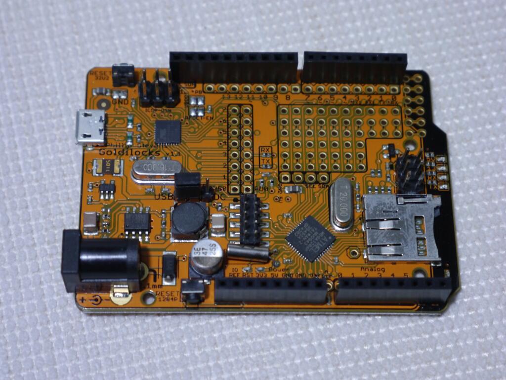
  • ATmega1284p @ 20MHz : Freetronics Goldilocks V1
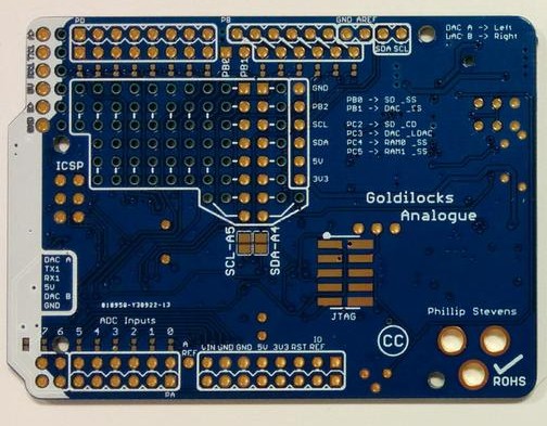
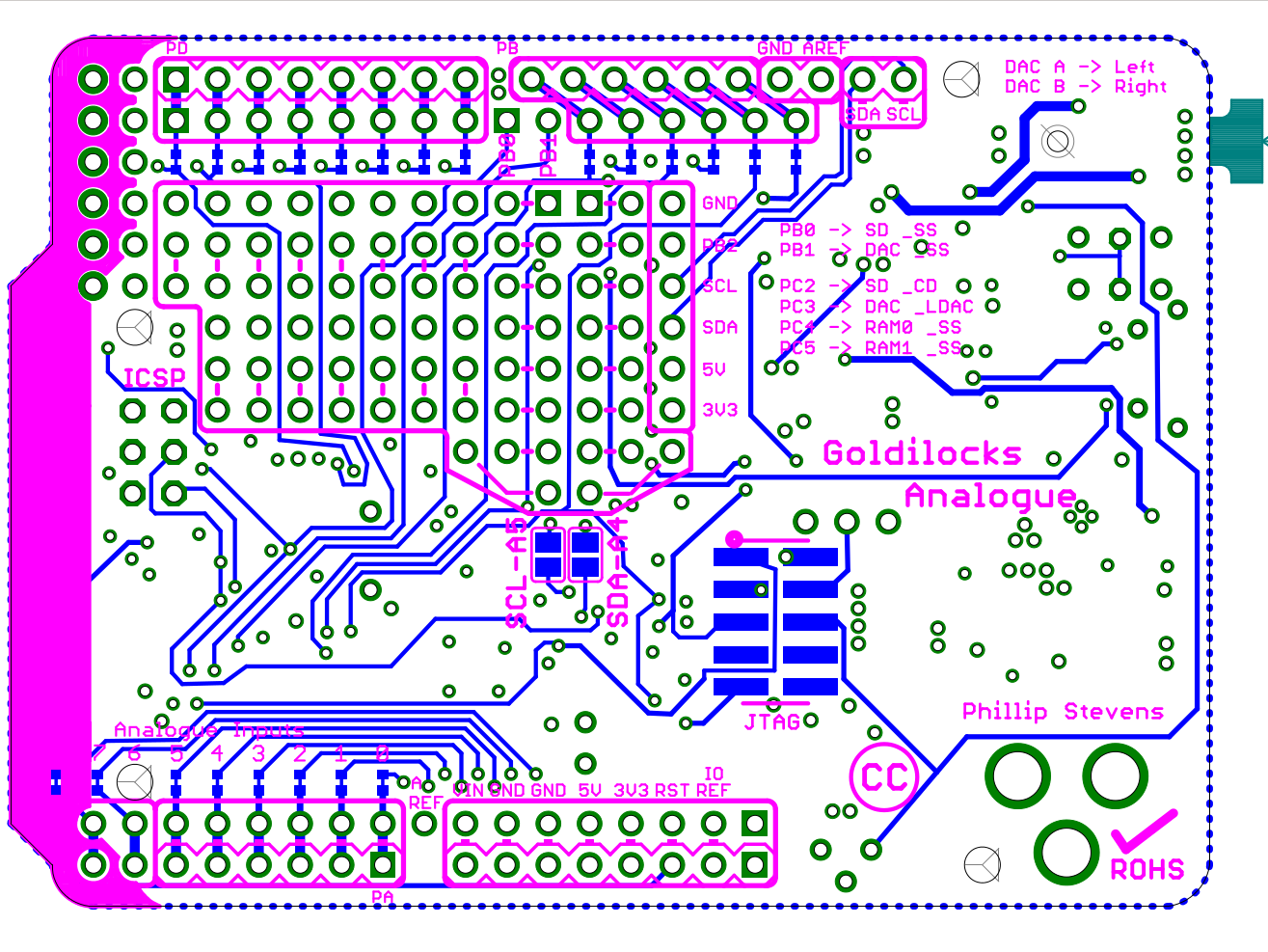
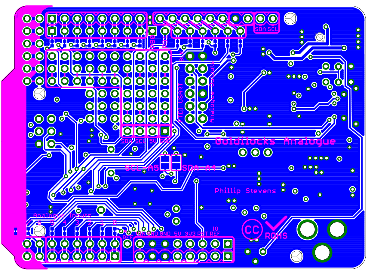
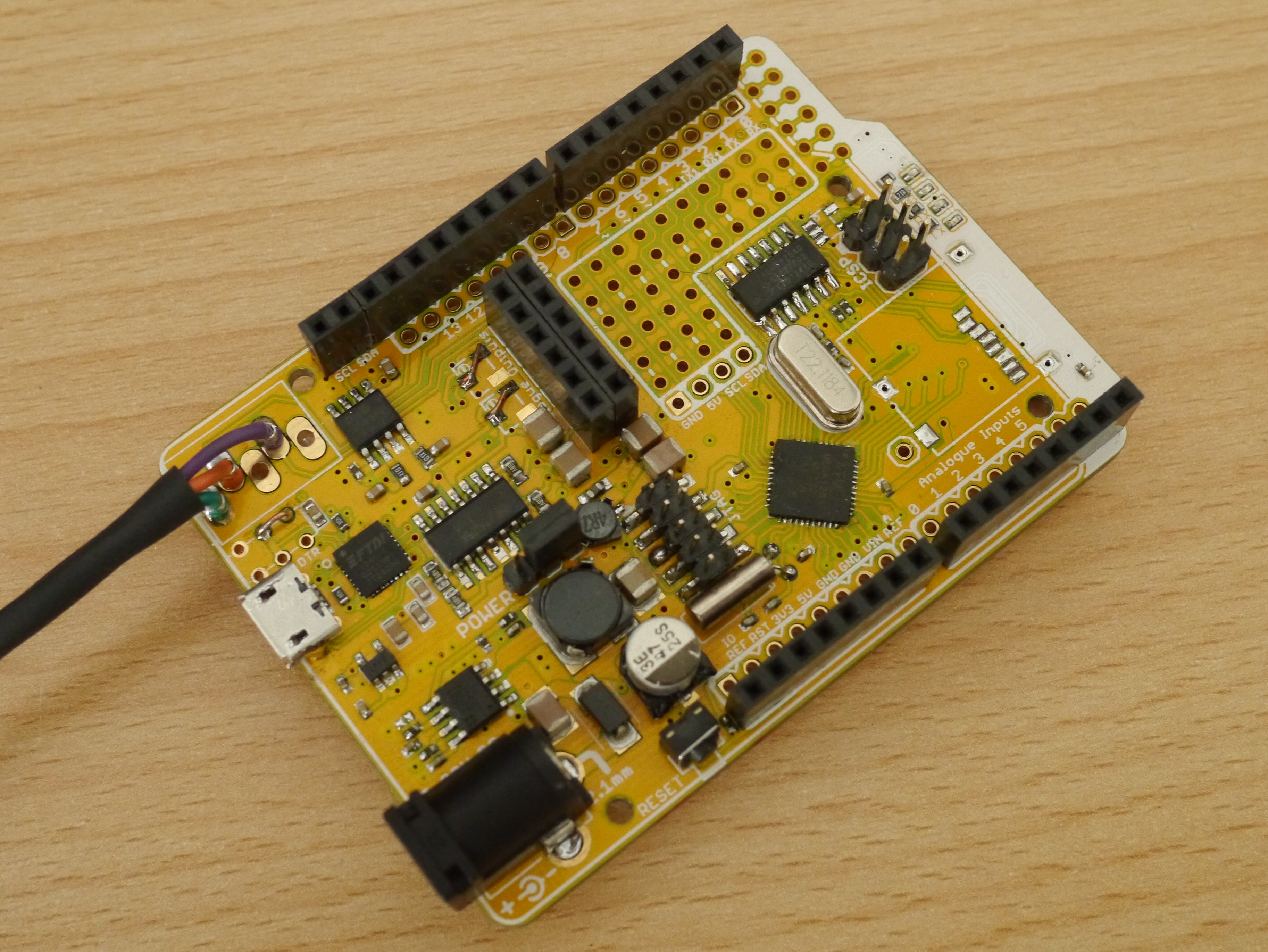
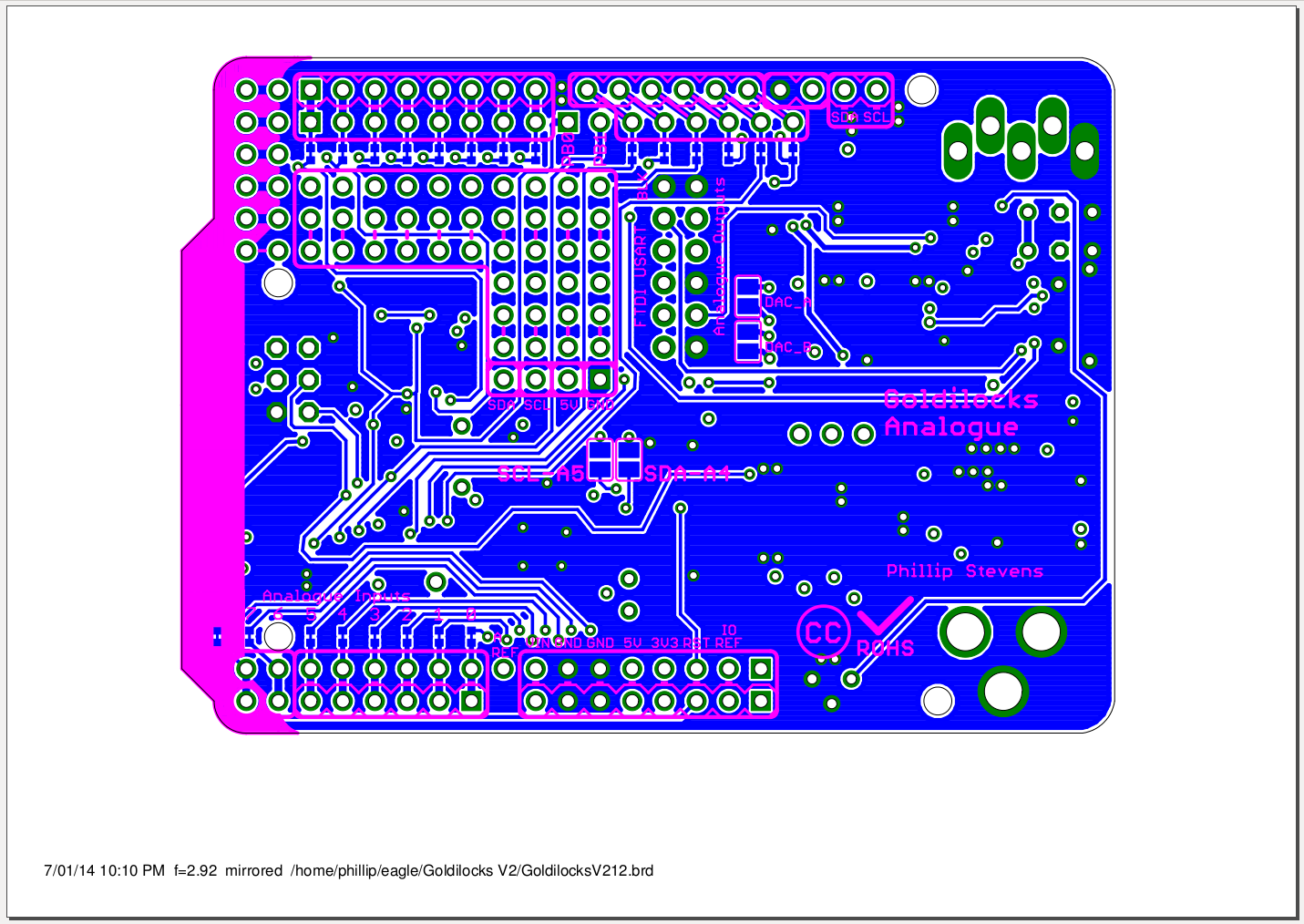
  • ATmega1284p @ 24.576MHz : Seeed Studio Goldilocks V2, Seeed Studio Goldilocks Analogue
  • ATmega2560 @ 16MHz : Arduino Mega, Arduino ADK
  • ATmega2560 @ 16MHz : Freetronics EtherMega
  • ATmega2560 @ 16MHz : Seeed Studio ADK
  • ATmegaXXXX @ XXMHz : Anything with an ATmega MCU, really.

Files and Configuration

  • Arduino_FreeRTOS.h : Must always be #include first. It references other configuration files, and sets defaults where necessary.
  • FreeRTOSConfig.h : Contains a multitude of API and environment configurations.
  • FreeRTOSVariant.h : Contains the AVR specific configurations for this port of FreeRTOS.
  • heap_3.c : Contains the heap allocation scheme based on malloc(). Other schemes are available and can be substituted (heap_1.c, heap_2.c, heap_4.c, and heap_5.c) to get a smaller binary file, but they depend on user configuration for specific MCU choice.

Goldilocks Analogue – Wrap Up

This is the final item on the Goldilocks Analogue as a design and production exercise.

Thank you for pledging on the Kickstarter Project page. Closed on November 19th 2015, with 124% funding. Now that the Kickstarter Pledges have been shipped, the Goldilocks Analogue is available on Tindie.

I sell on Tindie

I’ve been updating this post with the pre-production and production experience over the past few months.

The pre-production design materials, correcting the errata noted on Prototype Version 4, have been finalised and sent to Seeed Studio.
GoldilocksAnalogue_Seeed_20151120

The interim backer report is out, and now manufacturing quantities for procuring parts ready for the February production run have been finalised.

An updated version of the Goldilocks Analogue User Manual is available, and the Production Testing Document has reached Version 2 following inclusion of Windows 10 test procedures.

Revised Arduino IDE Variant files for Goldilocks Analogue using the Arduino core are available on Github.

Also additional optional libraries to provide support for each of the advanced features of the Goldilocks Analogue are available in the Arduino IDE Library Manager.

Arduino IDE compatibility testing revealed only a few remaining issues related to support of the ATmega1284p used in the Goldilocks Analogue. Two issues have been raised and resolved as 2 pull requests on the main Arduino IDE development path.

Both these issues have been committed into the Arduino main git tree, and they have landed in Arduino IDE Release 1.6.8.

The only remaining known issue is the limitation in the configuration of the Tones() code to use only Timer 2. We would like to use Timer 2 for the RTC. There is no other option but to use this Timer for the RTC support, so it would be good if Tones() could be configured to use a different timer.

Testing

Rather than going back over old ground, I’ll just be testing the pre-production version against the Version Prototype 4, to ensure that the things that should have improved, are improved, and that nothing has become broken.

Power Supplies

In the image below, Channel 1 (yellow) is 4.47mV of noise present at the output capacitor for the power supply, and Channel 2 (blue) is the 3.47mV supply noise present on a test Vcc pin closest to the MCU.

The significant improvement in noise level for the pre-production version at the MCU is similar to that achieved for the Prototype 4 (even slightly better), and this is probably due to reduced capacitive coupling into the ground plane by removing the ground copper from directly under the main supply inductor.

GA PP Power Supply Noise

GA PP: 5V Power Supply Noise

Remembering, for context, that 4mV is still the same order of the least significant bit for a 5V 10 bit ADC sampler, as found in the ATmega1284p, and a one bit change in the LSB of the MCP4822 input generates a 1mV change in output.

Checking the other power supplies on the board, Channel 1 (yellow) is the 3.3V positive supply, provided by a linear regulator. This supply is not used for analogue components, so the 4.0mV noise level is not critical, but never the less it is slightly less than on the Version P4.

Channel 2 (blue) below shows the -3V supply for the Operational Amplifier. This shows that the supply voltage noise of 5.9mV after filtering by a first order LC filter further smooth this supply. Compared to the Version P4 with no filtering (shown below) the noise is reduced substantially. The Version P4 shows a 10mV ramp, because it is a capacitive charge switching device. The addition of this LC filter was the one substantial change from the Prototype 4, so it is good to see the positive effect on the negative supply input to the Op Amp.

GA PP 3.3V and -3V Power Supply Noise

GA PP: 3.3V and -3V Power Supply Noise

Goldilocks Analogue Prototype 4 - 3.3V & -3V Supply Noise

GA P4: 3.3V & -3V Power Supply Noise

Analogue Output

The standard test that I’ve been using throughout the development is to feed in a 43.1Hz Sine wave generated from a 1024 value 16 bit LUT. The sampling rate is 44.1kHz, which is generated by Timer 1 to get the closest match.

The spectra and oscilloscope charts below can be directly compared to the testing done with prototype Version P4 and earlier versions of the Goldilocks Analogue.

The below chart shows the sine wave generated at the output of the Op Amp. This is exactly as we would like to see, with no compression of either the 4.096V peak, or the 0V trough.

Goldilocks Analogue – 43Hz Sine Wave – Two Channels – One Channel Inverted

GA PP: 43Hz Sine Wave – Two Channels – One Channel Inverted

Looking at the spectra generated up to 953Hz it is possible to see harmonics from the Sine Wave, and other low frequency noise.

The spectrum produced by the Goldilocks Analogue shows most distortion is below -70dB, and that the noise floor lies below -100dB. The pre-production sample shows slightly higher noise carriers than the Version P4, but the difference is not substantial.

GA PP 953Hz

GA PP: 43.1Hz Sine Wave – 953Hz Spectrum

In the spectrum out to 7.6kHz we are looking at the clearly audible range, which is the main use case for the device.

The Goldilocks Analogue has noise carriers out to around 4.5kHz, but they are all below -80dB. After 4.5kHz the only noise remains below -100dB.

GA PP 7k6Hz

GA PP: 43.1Hz Sine Wave – 7k6Hz Spectrum

The spectra out to 61kHz should show a noise carrier generated by the reconstruction frequency of 44.1kHz.

The Goldilocks Analogue shows the spectrum maintains is low noise level below -90dB right out to the end of the audible range, and further out to the reconstruction carrier at 44.1kHz.

GA PP 61kHz

GA PP: 43.1Hz Sine Wave –  61kHz Spectrum

The final spectrum shows the signal out to 976kHz. We’d normally expect to simply see the noise floor, beyond the 44.1kHz reconstruction carrier noise.

The Goldilocks Analogue has a noise carrier at around 210kHz, probably generated by the -3V supply. The noise carrier at 340kHz is generated through the 5V SMPS supply, and is absent when powered by USB socket. Aside from the two carriers mentioned, there is no further noise out to 976kHz.

GA PP 976kHz

GA PP: 43.1Hz Sine Wave – 976kHz Spectrum

The Pre-production analogue output works as specified, and is essentially identical to the analogue output on the Prototype 4. It can maintain the 72dB SNR required, of which it should theoretically be capable.

Goldilocks Analogue Synthesizer

For the past year, I’ve been prototyping an Arduino clone, the Goldilocks Analogue, which incorporates advanced analogue output capabilities into the design of the original Goldilocks with ATmega1284p AVR MCU and uSD card cage. Recently the design scope crept up to include two SPI memory devices (EEPROM, SRAM, FRAM), and microphone audio input. But, before I go through another prototype cycle, I thought it would be a good idea to build some demonstration applications, showcasing the capabilities of an arduino R3 compatible platform with integrated analogue output and have some fun with audio.

Goldilocks Analogue Prototype 3

Some of the initial tests I’ve built include some 8 bit algorithmic music and, using two Goldilocks Analogue prototype devices, a digital walkie talkie using Xbee radios. They were fun, but don’t really demonstrate the full range of the audio capabilities of the platform.

It seemed appropriate to build a synthesizer using the Goldilocks Analogue as the platform, and a Gameduino 2 shield incorporating a FDTI FT800 EVE GPU, and see how close I could get to a musical outcome.

Research

Before randomly building something that made a bunch of squeaky sounds, I thought the best thing to do is to learn something about the field of analogue synthesizers and synthesizing audio.

I also obtained some simple analogue synthesizers from Korg to see exactly what they produce, so I could copy them. Some people write that this monotron analogue synthesizer family are good examples of a low cost musical instrument. I found it very interesting to examine the wave forms produced by the various settings.

Using the features of the two Korg devices, I was able to define the goal for the synthesizer that I wanted to build using the Goldilocks Analogue.

The Korg monotron DUO has two voltage controlled oscillators (VCO1 and VCO2), which produce square waves. The VCO1 has a pitch setting, which defines the basic frequency at which the ribbon keyboard operates. The ribbon keyboard can be set to have a major scale, a minor scale, a full chromatic scale, or be a ribbon with no set notes. For clarity, the pitch on the DUO is analogue, so there is no guarantee that the notes generated by the ribbon keyboard will be in tune.

The VCO2 pitch can be modified either below or above the pitch of the VCO1. In its middle section, with some care, it can be matched exactly to the VCO1 setting. The switch allows either just the VCO1 or both VCO1 and VCO2 to produce sound. A separate XMOD intensity knob allows the VCO2 to modulate the frequency of the VCO1 oscillator, producing cross-modulation.

The monotron DUO contains the famous Korg MS-20 resonant low pass filter, which can be adjusted for both cut-off frequency and intensity of the resonant frequency. Setting the filter values allows the square wave noise generated by the two oscillators to be shaped into very interesting tones.

The Korg monotron DELAY is a very different device from the DUO. It has two oscillators, but only one at audio frequencies. The audio oscillator produces a saw-tooth wave at a frequency controlled by the ribbon keyboard. On the monotron DELAY there is no capability for playing specific notes as the keyboard is only available in ribbon mode. The second oscillator of the monotron DELAY is a low frequency oscillator (LFO), which can be adjusted from 1Hz up to about 30Hz. This LFO can produce either a triangle wave or a square wave to modulate the main audio oscillator. This is used mainly to apply vibrato to musical tones, or to produce very unusual tone ramps. The intensity and pitch of the LFO are controlled by knobs.

The Korg low pass filter present in the monotron DELAY is only adjustable for its cutoff frequency, so it is less flexible and interesting than the monotron DUO implementation.

The monotron DELAY is really built to showcase the analogue space delay functionality, which can be adjusted in both length of delay, and in intensity of feedback. With about 1 second of delay and 100% or more feedback possible, very short sequences of notes can be played and then built upon.

I’m not particularly musical, but I spent some very pleasant hours playing with the two Korg synthesizers experimenting with the sounds available from their very simple platforms, and used their capabilities to guide me in what to build into my Goldilocks Analogue synthesizer.

The next piece of research was to understand how to generate analogue wave forms using direct digital synthesis, and then how to modify sound of the wave forms using convolution or modulation in the time domain.

Design Specification

Having the two Korg devices as an inspiration, and reading about the original Moog synthesizer capabilities from the 1970’s, made the specification pretty straight forward.

Goldilocks Analogue GUI

The Goldilocks Analogue synthesizer has three oscillators, two of which operate at audio frequencies, being VCO1 and VCO2, and one low frequency oscillator, being LFO. The VCO1 is tuned in octaves at correct concert pitch, so that notes played would be at the right frequency. The VCO2 is pitched relative to the VCO1 pitch, and would range minus one octave to plus one octave (or half the VCO1 frequency to double the VCO1 frequency). The LFO is adjustable over the range from 1 Hz to 40 Hz.

I had decided to let each oscillator take one of two wave forms. For VCO1 I initially chose square wave, and saw tooth wave, to be able to replicate the exact sound of the Korg devices. I’ve since decided to move the saw tooth wave to the VCO2, and replaced it with a sine wave on VCO1. It is good to have the pure tone at the correct frequency for tuning instruments. An A4 from the Goldilocks Analogue Synthesizer will, for example, always be 440Hz.

For VCO2 I selected a triangle wave and a saw tooth wave. And, for the LFO there is a sine wave and a triangle wave available. I should point out that changing the wave form available to each oscillator is no more complicated that replacing the look-up table associated with the setting, and there is space available in the ATmega1284p to store at least another 4 separate wave form tables in flash memory, even without extending to on-board SPI EEPROM, or uSD storage.

In the mixing section the intensity or volume of each of VCO1 and VCO2 can be set. It is possible to turn off either oscillator. The intensity of the LFO effect is controlled too. The LFO modulates both the VCO1 and the VCO2. The final input is the cross modulation of VCO1 by the VCO2. Very interesting tonality is created by modulating VCO1 by pitches very close to its own frequency.

Each note is put through an exponential Attack and Release envelope, to give the note some shape. The mixed signal is then be sent to the voltage controlled filter. Using the current set up, the sample rate is 16,000 samples/second, which is enough to produce 6 octaves. The upper two octaves remain implemented, but are not reconstructed accurately. I have implemented a Biquad IIR filter to enable the output to be high, low, or band pass filtered. The default set up is for low pass filtering. The filter -3dB frequency, and the ringing levels can be adjusted for different musical effect.

Following the filter stage, the signal enters the space delay stage. The space delay stage can have only about half a second of delay, because of the RAM limitations (16kByte) of the ATmega1284p. So up to 6700 16 bit samples are supported by the space delay function. Samples are recovered from the delay buffer, and mixed with the new signals, then injected back into the delay loop. This creates an infinite loop of samples, depending on the amount of feedback set by the FEEDBACK control.

The final signal output level is controlled by a MASTER volume control. Additionally, an EEPROM STO and RCL capability for the settings has been implemented. Only the most recent settings are stored, which can be recalled when power is restored.

As the keyboard notes are generated using a look up table, multiple keyboard tuning options are possible. I have implemented Concert Tuning (A4 = 440Hz) and Equal Temperament (commonly used for pianos), and Verdi or Stradivari tuning (C4 = 256Hz) with Just Intonation Equal Fifths as an alternative. There is a toggle to chose between either these two options. Any tuning can be generated, and then loaded as the note table.

GUI Implementation

The GUI of the solution depends on a Gameduino 2 screen, which is based on the FTDI Chip FT800 EVE GPU device. The FT800 was the first EVE GPU available from FTDI and it can only support single touch. This limitation makes it only partially useful as a product to support this application. The most interesting sounds are generated by bending the controls whilst playing the notes. Fortunately there are newer EVE GPU devices that support multi-touch and they would make a better platform if this synthesizer were to become more than just a demonstration.

The GUI makes extensive use of FT800 co-processor widget capabilities being dials, toggles, keys, and text. Some examples below.

// text
FT_GPU_CoCmd_Text_P(phost, 300,  8, 27, OPT_CENTER, PSTR("VCF"));
FT_GPU_CoCmd_Text_P(phost, 300, 25, 26, OPT_CENTER, PSTR("CUTOFF"));
FT_GPU_CoCmd_Text_P(phost, 300, 95, 26, OPT_CENTER, PSTR("PEAK"));

// toggles
FT_API_Write_CoCmd(TAG(LFO_WAVE));
FT_GPU_CoCmd_Toggle_P(phost, 13,242,46,18, OPT_3D, synth.lfo.wave, PSTR("SIN" "\xFF" "TRI"));

FT_API_Write_CoCmd(TAG(KBD_TOGGLE));
FT_GPU_CoCmd_Toggle_P(phost, 405,130,60,26, OPT_3D, synth.kbd_toggle, PSTR("CONCRT" "\xFF" "VERDI"));

// dials
FT_API_Write_CoCmd(TAG(DELAY_FEEDBACK));
FT_GPU_CoCmd_Dial(phost, 365,125,20, OPT_3D, synth.delay_feedback); // DELAY FEEDBACK

FT_API_Write_CoCmd(TAG(MASTER));
FT_GPU_CoCmd_Dial(phost, 440,55,26, OPT_3D, synth.master); // MASTER

The integrated touch tracking capability makes it very easy to parse touch into specific commands.

readTag = FT_GPU_HAL_Rd8(phost, REG_TOUCH_TAG);

if (readTag > 0x80)// tag is greater than 0x80 and therefore is a dial.
{
	TrackRegisterVal.u32 = FT_GPU_HAL_Rd32(phost, REG_TRACKER);

	switch (TrackRegisterVal.touch.tag)
	{
	case (VCO1_PITCH):
		synth.vco1.pitch = TrackRegisterVal.touch.value & 0xe000;
		break;
	// continues...
	}

This integrated touch tracking capability can return which dial (slider / scroll bar) has been touched, and the relative position of the touch. This same position value can then be used in the display command to set the position of the dial (slider / scroll bar), providing direct feedback on the GUI.

The main GUI task simply calls the touch function, and if there is a touch recorded the GUI is updated, and the revised settings entered into the analogue audio control structure. Otherwise if there are no touches recorded there are no processor cycles wasted updating the display. The FT800 EVE GPU continues to display the same content until a new display list is loaded into the GPU memory.

When a keyboard touch is recorded, the tone generation information is updated, and this then directly impacts the output tone generated by the audio section.

//  setting the phase increment for VCO1 is frequency * LUT size / sample rate.
//  << 1 in SAMPLE_RATE is residual scale to create 24.8 fixed point number.
// The LUT is already pre-scaled << 7 in the calculation.
// The LUT can't be pre-scaled to << 8 because this creates numbers too large for uint32_t to hold,
// and we want to allow the option to vary the SAMPLE_RATE at compilation time, so it has to stay in the calculation.
synth.vco1.phase_increment = (uint32_t)pgm_read_dword(synth.note_table_ptr + stop * NOTES + note) / (SAMPLE_RATE >> 1);

// set the VCO2 phase increment to be -1 octave to +1 octave from VCO1, with centre dial frequency identical.
if (synth.vco2.pitch & 0x8000) // upper half dial
	synth.vco2.phase_increment = ((synth.vco1.phase_increment >> 4) * synth.vco2.pitch ) >> 11;
else // lower half dial
	synth.vco2.phase_increment = (synth.vco1.phase_increment >> 1) + (((synth.vco1.phase_increment >> 4) * synth.vco2.pitch) >> 12);

// set the LFO phase increment to be from 0 Hz to 32 Hz.
synth.lfo.phase_increment = ((uint32_t)synth.lfo.pitch * LUT_SIZE / ((uint32_t)SAMPLE_RATE << 4) );

The phase increment desired, respective to the relevant tone desired, is read from a look up table containing 8 octaves each of 12 notes for VCO1. VCO2 phase increment is then set as a proportion of VCO1. And LFO phase increment is set to range from 0 to around 30 Hz. With this information, and the selected wave form look up table, the audio implementation can do its thing.

Audio Implementation

The synthesizer audio section is implemented in one function, that is executed each time a new sample is generated. This means at 12,000 samples/ second sample generation frequency, we have 83 micro seconds to generate the final sample to be pushed to the Goldilocks Analogue MCP4822 12 bit dual channel DAC.

The current sample generation routine takes under 45 micro seconds to complete with 3 Oscillators running, so there is a little head room still available. With some further coding improvements it was possible to raise the sample frequency to 16,000 samples/sec as the sample generation frequency. The below logic trace shows the main SPI interface (SCK, MISO, MOSI, _SS) delivering commands to the EVE GPU, and the lower MSPI interface (MSPI SCK, MSPI MOSI, MSPI PING) providing the calculated samples, every 83 micro seconds, to the DAC.

Goldilocks Analogue Synthesizer, with 3 Oscillators operating.

Goldilocks Analogue Synthesizer, with 3 Oscillators operating.

It is clear to see that two EVE GPU transactions are being interrupted by the DAC output, but because the main SPI interface is not changing state the transaction is faultlessly resumed once the DAC interrupt is completed.

In contrast, when there are no oscillators running because no key is pressed, the sample generation routine takes just 28 micro seconds to complete. The logic trace below shows the change of state from 0 to 3 oscillators.

Goldilocks Analogue, with no Oscillators operating.

Goldilocks Analogue, with no Oscillators operating.

There is little time available to calculate sample values in real time, so all of the samples are pre-calculated and are stored in look-up tables (LUT). Each LUT contains 4096 16 bit samples, which gives 12 significant bits of accuracy for the values. I chose 4096 samples because the ATmega1284p has sufficient storage to support multiple tables of this size in its flash memory. Smaller LUTs would sacrifice accuracy, and larger LUTs would compromise on the number of available wave forms.

I have prepared LUTs for sine wave, square wave, triangle wave, and saw tooth wave options. Another advantage of the LUT approach is that better bandwidth optimised LUT values can be substituted without changing the code. Also, LUTs allow completely arbitrary waveforms could be used if desired to obtain specific timbre or nuances of sound.

The sample generation code starts with the LFO oscillator using a direct digital synthesis model. Each oscillator sample is calculated identically by stepping through the LUT with a phase increment based on the frequency of the note required, but VCO2 phase increment is modified by the LFO output and the VCO1 phase increment is modified by both VCO2 and LFO outputs.

Code shown here assumes that both LFO and VCO2 output wave forms have already been calculated.

///////////// Now do the VCO1 ////////////////////

// This will be modulated by the VCO2 value (depending on the XMOD intensity),
// and the LFO intensity.
if( synth.vco1.toggle )
{
	// Increment the phase (index into waveform LUT) by the calculated phase increment.
	// Both the phase and phase_increment are stored as 24.8 in uint32_t.
	// The fractional component of the phase and phase_increment is needed to ensure the wave
	// is tracked accurately.
	synth.vco1.phase += synth.vco1.phase_increment;

	// calculate how much the LFO affects the VCO1 phase increment
	if (synth.lfo.toggle)
	{
		// increment the phase (index into LUT) by the calculated phase increment including the LFO output.
		synth.vco1.phase += (uint32_t)outLFO; // increment on the fractional component 8.8, limiting the effect.
	}

	// calculate how much the VCO2 XMOD affects the VCO1 phase increment
	if (synth.vco2.toggle)
	{
		// increment the phase (index into LUT) by the calculated phase increment including the LFO output.
		synth.vco1.phase += (uint32_t)outXMOD; // increment on the fractional component 8.8, limiting the effect.
	}

	// if we've gone over the waveform LUT boundary -> loop back
	synth.vco1.phase &= 0x000fffff; // this is a faster way doing the table
						// wrap around, which is possible
						// because our table is a multiple of 2^n.
						// Remember the lowest byte (0xff) is fractions of LUT steps.
						// The table is 0xfff.ff bytes long.

	currentPhase = (uint16_t)(synth.vco1.phase >> 8); // remove the fractional phase component.

	// get first sample from the defined LUT for VCO1 and store it in temp1
	temp1 = pgm_read_word(synth.vco1.wave_table_ptr + currentPhase);
	++currentPhase; // go to next sample

	currentPhase &= 0x0fff;	// check if we've gone over the boundary.
				// we can do this because it is a multiple of 2^n.

	// get second sample from the LUT for VCO1 and put it in temp2
	temp2 = pgm_read_word(synth.vco1.wave_table_ptr + currentPhase);

	// interpolate between samples
	// multiply each sample by the fractional distance
	// to the actual location value
	frac = (uint8_t)(synth.vco1.phase & 0x000000ff); // fetch the lower 8bits

	// the optimised assembly code Multiply routines come from Open Music Labs.
	MultiSU16X8toH16Round(temp3, temp2, frac);

	// scaled sample 2 is now in temp3, and since we are done with
	// temp2, we can reuse it for the next result
	MultiSU16X8toH16Round(temp2, temp1, 0xff - frac);
	// temp2 now has the scaled sample 1
	temp2 += temp3; // add samples together to get an average
	// our resultant wave is now in temp2

	// set amplitude with volume
	// multiply our wave by the volume value
	MultiSU16X16toH16Round(outVCO1, temp2, synth.vco1.volume);
	// our VCO1 wave is now in outVCO1
}

The next piece of the audio process is to mix the two oscillators VCO1 and VCO2, and then calculate the space delay required. This is where the resonant low pass filter is implemented.

////////////// mix the two oscillators //////////////////
// irrespective of whether a note is playing or not.
// combine the outputs
temp1 = (outVCO1 >> 1) + (outVCO2 >> 1);

///////// Resonant Low Pass Filter here  ///////////////
IIRFilter( &filter, &temp1);

///////// Do the space delay function ///////////////////

// Get the number of buffer items we have, which is the delay.
MultiU16X16toH16Round( buffCount, (uint16_t)(sizeof(int16_t) * DELAY_BUFFER), synth.delay_time);

// Get a sample back from the delay buffer, some time later,
if( ringBuffer_GetCount(&delayBuffer) >= buffCount )
{
	temp0.u8[1] = ringBuffer_Pop(&delayBuffer);
	temp0.u8[0] = ringBuffer_Pop(&delayBuffer);
}
else // or else wait until we have samples available.
{
	temp0.i16 = 0;
}

if (synth.delay_time) // If the delay time is set to be non zero,
{
	// do the space delay function, irrespective of whether a note is playing or not,
	// and combine the output sample with the delayed sample.
	temp1 += temp0.i16;

	// multiply our sample by the feedback value
	MultiSU16X16toH16Round(temp0.i16, temp1, synth.delay_feedback);
}
else
	ringBuffer_Flush(&delayBuffer);	// otherwise flush the buffer if the delay is set to zero.

// and push it into the delay buffer if buffer space is available
if( ringBuffer_GetCount(&delayBuffer) <= buffCount )
{
	ringBuffer_Poke(&delayBuffer, temp0.u8[1]);
	ringBuffer_Poke(&delayBuffer, temp0.u8[0]);
}
// else drop the space delay sample (probably because the delay has been reduced).

////////////// Finally, set the output volume //////////////////
// multiply our wave by the volume value
MultiSU16X16toH16Round(temp2, temp1, synth.master);

// and output wave on both A & B channel, shifted to (+)ve values only because this is what the DAC needs.
*ch_A = *ch_B = temp2 + 0x8000;

This generates the required output waveforms that make the Goldilocks Analogue Synthesiser work.

The second order Biquad IIR filter code has been implemented in a general way, enabling multiple filters to be applied to the sample train. Set up for Low Pass, Band Pass, and for High Pass have been implemented. The coefficients and state variables for each filter are maintained in a structure.

//========================================================
// second order IIR -- "Direct Form I Transposed"
//  a(0)*y(n) = b(0)*x(n) + b(1)*x(n-1) +  b(2)*x(n-2)
//                   - a(1)*y(n-1) -  a(2)*y(n-2)
// assumes a(0) = IIRSCALEFACTOR = 32 (to increase calculation accuracy).

// http://en.wikipedia.org/wiki/Digital_biquad_filter
// https://www.hackster.io/bruceland/dsp-on-8-bit-microcontroller
// http://www.musicdsp.org/files/Audio-EQ-Cookbook.txt

typedef struct {
	uint16_t sample_rate;	// sample rate in Hz
	uint16_t cutoff;	// normalised cutoff frequency, 0-65536. maximum is sample_rate/2
	uint16_t peak;		// normalised Q factor, 0-65536. maximum is Q_MAXIMUM
	int16_t b0,b1,b2,a1,a2;	// Coefficients in 8.8 format
	int16_t xn_1, xn_2;	//IIR state variables
	int16_t yn_1, yn_2;	//IIR state variables
} filter_t;

void setIIRFilterLPF( filter_t *filter ) // Low Pass Filter Setting
{
	if ( !(filter->sample_rate) )
		filter->sample_rate = SAMPLE_RATE;

	if ( !(filter->cutoff) )
		filter->cutoff = UINT16_MAX >> 1; // 1/4 of sample rate = filter->sample_rate>>2

	if ( !(filter->peak) )
		filter->peak =  (uint16_t)(M_SQRT1_2 * UINT16_MAX / Q_MAXIMUM); // 1/sqrt(2) effectively

	double frequency = ((double)filter->cutoff * (filter->sample_rate>>)) / UINT16_MAX;
	double q = (double)filter->peak * Q_MAXIMUM / UINT16_MAX;
	double w0 = (2.0 * M_PI * frequency) / filter->sample_rate;
	double sinW0 = sin(w0);
	double cosW0 = cos(w0);
	double alpha = sinW0 / (q * 2.0f);
	double scale = IIRSCALEFACTOR / (1 + alpha); // a0 = 1 + alpha

	filter->b0	= \
	filter->b2	= float2int( ((1.0 - cosW0) / 2.0) * scale );
	filter->b1	= float2int(  (1.0 - cosW0) * scale );

	filter->a1	= float2int( (-2.0 * cosW0) * scale );
	filter->a2	= float2int( (1.0 - alpha) * scale );
}

// interim values in 24.8 format
// returns y(n) in place of x(n)
void IIRFilter( filter_t *filter, int16_t * xn )
{
	int32_t yn;	// current output
	int32_t  accum;	// temporary accumulator

	// sum the 5 terms of the biquad IIR filter
	// and update the state variables
	// as soon as possible
	MultiS16X16to32(yn,filter->xn_2,filter->b2);
	filter->xn_2 = filter->xn_1;

	MultiS16X16to32(accum,filter->xn_1,filter->b1);
	yn += accum;
	filter->xn_1 = *xn;

	MultiS16X16to32(accum,*xn,filter->b0);
	yn += accum;

	MultiS16X16to32(accum,filter->yn_2,filter->a2);
	yn -= accum;
	filter->yn_2 = filter->yn_1;

	MultiS16X16to32(accum,filter->yn_1,filter->a1);
	yn -= accum;

	filter->yn_1 = yn >> (IIRSCALEFACTORSHIFT + 8); // divide by a(0) = 32 & shift to 16.0 bit outcome from 24.8 interim steps

	*xn = filter->yn_1; // being 16 bit yn, so that's what we return.
}

Hardware Implementation

I sell on Tindie

The Goldilocks Analogue Prototype 3 is working very well, and it has resolved some of the issues of the second prototype. Using the USART1 MSPIM mode to drive the MCP4822 DAC allows the GUI to use the SPI bus for the Gameduino 2 GUI without conflicts. This is the only way that the rigorous timing for audio output can be maintained, given the heavy SPI usage required to drive the GPU co-processor.

Goldilocks Analogue - Prototype 3

The Atmel AVR ATmega1284p in the Goldilocks Analogue Prototype 3 is running at 24.576MHz. This is significantly above the specification (20MHz at 5V), but remembering that the specification for AVR ATmega devices covers an extended temperature range (that would kill a human) and it is unlikely that the Goldilocks Analogue would be used in extreme temperature situations, I’ve had no problems with this processor frequency to date.

There are two reasons for over-clocking the ATmega1284p. The first is that it is simply not possible to make the required calculations within the time budget available at the maximum specification CPU frequency of 20MHz or even more extreme at the standard Arduino rate of 16MHz.

The second reason is related to the generation of exact audio sampling frequencies. With a CPU clock of 24.576MHz, the 8 bit timer with pre-scaling can generate EXACT audio sample timing at 8kHz, 12kHz, 16kHz, 32kHz, and 48kHz. Using a 16 bit timer, we can also generate very close approximations to 44.1kHz, if required.

The routine to transfer samples does not need to consume precious 16 bit timer resources, which are useful to produce PWM for motor control. Retaining the capability to manage two motors (using the two 16 bit timers) is fairly important outcome.

The interrupt for generating the wave forms does only two things; write the sample values to the DAC, and then calculate the new sample value for the next sample time. The samples are written to the DAC first to ensure that the output is not jittered by the possibility of variable processing time in the audio handler routine. This can happen if (for example) one of the VCO is turned off, removing the sample calculation code from the code execution path.

ISR(TIMER0_COMPA_vect) __attribute__ ((hot, flatten));
ISR(TIMER0_COMPA_vect)
{
	// MCP4822 data transfer routine
	// move data to the MCP4822 - done first for regularity (reduced jitter).
	// &'s are necessary on data_in variables
	DAC_out (ch_A_ptr, ch_B_ptr);

	// audio processing routine - do whatever processing on input is required - prepare output for next sample.
	// Fire the global audio handler, if set.
	if (audioHandler!=NULL)
		audioHandler(ch_A_ptr, ch_B_ptr);
}

Goldilocks Analogue – Prototyping 3

The Prototype 4 has now been designed, read here for the next iteration. I’ve received the Prototype 4 back and now I’m testing them.

Following my initial design article, and the follow up design article, I’ve put quite a lot of thought into how I can make this Goldilocks Analogue device best achieve my stated goals. Pictured is the new 3rd Goldilocks Analogue Prototype

Goldilocks Analogue Prototype 3

The finished prototype boards are now in my hands, and testing of the PCB configuration the new SPI EEPROM and SRAM capabilities, together with MSPIM interface for the DAC begins. These two features contribute to making the Goldilocks Analogue great analogue synthesiser platform.

P1010913

Combined with a Gameduino2 LCD and touch screen, it creates flexible sound touch controller, with quality analogue output.

Goldilocks Analogue - Prototype 3

Goldilocks Analogue – Prototype 3

This is the working design document. It will grow as I get more stuff done, and notes added here. I’ve pretty much finished the paper design now, and will let it settle for a few weeks over the 2014 holiday season. It is sometimes good to do things again, with a few weeks perspective from the original decisions.

Goldilocks Analogue - Prototype 2

Goldilocks Analogue – Prototype 2

Major Revision in Strategy

Over the past months I’ve been spending time writing code to go along with the latest revision of the Goldilocks Analogue. I have successfully implemented a version of the NASA EEFS simple flash file system, to use to buffer data either for acquisition or for analogue playback, and I’ve been working on streaming functions to get data off the SD card and off the EEFS flash file system. The outcome is that it is not possible to do everything with just one SPI bus, and keep generality when needed. The SD card is just too slow, and can’t be easily interrupted. The FRAM/SRAM/EEPROM doesn’t have enough storage to effectively stream GigaBytes of data, as a uSD card can achieve.

So, what to do? Adafruit uses a software bit-banged SPI outcome to drive their MCP4921 and doesn’t get close to the maximum speed I want to achieve. Fortunately, with the ATmega1284p there is a simple answer at hand. I have decided to move the MCP4822 off the standard SPI pins, and connect it to the USART1 TX and XCK pins, using the USART in its Master SPI mode.

This is a major revision in strategy. Previously I have been very adverse to putting anything on the standards Arduino pins, preferring to keep all of the Goldilocks extra features off the Arduino footprint. However, the outcome is well worth using the USART1 to drive the MCP4822, and nothing is compromised.

USART MSPI mode is available on any ATmega device. On the UNO platform, using the ATmega328p, there is only one USART and so of course it is reserved for serial communications. The Goldilocks ATmega1284p has two USART interfaces, and usually the second one (USART 1) goes unused. Therefore connecting its XCK and TX pins to the MCP4822 is the simplest and best outcome to achieve high throughput and regularity SPI output on a non-shared SPI interface. And, as the MCP4822 DAC has high impedence (~10kOhm) inputs, having the DAC sharing the pins won’t affect normal pin usage to any extent.

And, there’s more win. The USART MSPI has double buffering for the transmit function. This means that we can actually achieve a higher throughput using the USART MSPI than we can using the standard SPI bus! These logic traces demonstrate that the my best implementation of the SPI interface requires 4.58us to transmit a “frame” of information, consisting of two 12 bit samples. Using the USART MSPI interface we can achieve 4.25us per frame.

DAC control using SPI bus.

DAC control using SPI bus.

DAC control using SPI bus.

DAC control using USART MSPI bus.

Either way, achieving 44.1kHz stereo output is not an issue. This trace shows the time spent in the DAC-out interrupt for a simple function, with the samples being played out at 44.1kHz.

44.1kHz samples using USART MSPI output.

44.1kHz samples using USART MSPI output.

Guessing that this would be a great outcome, I ordered new PCBs from Seeed which implement the new pin assignments for the MCP4822. They will be here shortly.

My Revision Plans

Revert the uSD card 3V SPI bus drivers back to the quad and single buffers. The TXB/TXS story remains unresolved, and I can’t be bothered to work out why, when a simple answer is at hand. – DONE

Connect the uSD _CARD_DETECT to PC2 which has no other function except JTAG. – DONE

Remove the FTDI 6 pin for USART0. Or, better to move it to connect to USART1, so that USART1 can be addressed by an external FTDI device. Move it to the end of the board, so it doesn’t block Shield usage. Note the RTS/CTS Reset is not connected because this is replaced by a DAC A/B channel. – DONE

Remove the Analogue outputs from centre of board. Move them to the end of the board and integrate them into the FTDI USART1 socket on the RTS and CTS pin positions (obviously not on Tx or Rx pins, or on Vcc or GND either). – DONE

Connect the MCP4822 _LDAC pin to enable sychronisation of the A and B channels. Connect to PC3 which has no other function except JTAG. Remember the _LDAC is pulled to GND by default. – DONE

Have another look at the output filtering on the DAC, perhaps it could be a little stronger than the prototype with the corner at 23kHz. Single pole R1=68Ω C1=100nF. – DONE

This 2nd order filter is still linear, but filters significantly more (6dB rather than 3dB per decade) than the single pole version on the prototype.

2nd Order RC Low Pass Filter

Using standard Resistor and Capacitor values R1=47Ω C1=100nF R2=47Ω C2=100nF in a 2nd order CR Low-pass Filter Design Tool.

Extend the prototyping area by three columns. – DONE

Add a pin-out to allow the DS3231 RasPi module (battery or super capacitor) from Seeed Studio to be easily attached. Unfortunately, the devices I have don’t implement an _INT/SQW output, so alarms and wake on alarm won’t be possible. – DONE

Push the JTAG pads to the back of the board, without forgetting to flip the pin layout around. – DONE

Add SRAM or FRAM SPI storage. FRAM is non volatile storage, that has no delay. With a reasonable amount of storage we can use it to provide short audio samples, and get them back relatively easily, without file system and uSD card overheads. But FRAM is pretty expensive, and SRAM chips with same pin-out are available for much cheaper, that might fulfil the job of buffering or capturing samples.

MB85RS64V FRAM is the only reasonable device available for 5V supply. And it is a reasonable price of $1.80 per unit. But it is much too small to use as an analogue sample store. Need to use the 128kB MB85RS1MT FRAM version, but this required being driven from Vcc 3V3. At 8kHz sampling, 128kB gives us 16 seconds of sound, which is quite a lot. It costs around $6 which seems to be the sweet spot in pricing now. Will have to add another 3V3 to 5V MISO buffer. Use PC4 as the MB85RS1MT SPI _SS line.

Alternatively, just make the pinout for SPI 5V and implement SRAM using the Microchip 23LC1024 device, which is $2.50 each. We can choose FRAM or SRAM at assembly. Or even both, as there is a spare _SS available. So let’s do two devices at Vcc 5V supply.

Put 10kOhm pull-up resistors on all of these _SS lines, _CARD_DETECT and _HOLD. – DONE

Add 10kOhm pull-down resistors on _LDAC allowing active _LDAC control but not requiring it. – DONE

Convert the 3.3V regulator to AP1117 type in SOT89-3 package. No space for SOT223. Upgrades the 3.3V supply from 150mA to 1000mA. Heat spread on Layer 2 GND and on Layer 15. – DONE

Initial Board Layout

I’ve finished the schematic and the board layout, and now I just have the detailed work of checking all the things, again, and again. I’ve come back to this after letting it stew for a few days with the thought of changing just one component. But, as usual have made a host of minor adjustments that should make it better. These include further clearance of the ground plane under the analogue components, and untangling and straightening signals and vias where possible.

The Goldilocks Analogue Schematic  in PDF format.

Front of board (All Layers)

The board is now pretty tightly packed. But, there is still a large number of options for prototyping on the board, or to exit the board with 8-pin headers. Each of Port A, Port B and Port D can be taken off board with one header each. Alternatively, a 2×8 connector can be attached, with the pins assigned and connected as desired.

The DAC A (L) and DAC B (R) channels are integrated into the far right edge of the board, along with TX1 and RX1 pins in the form of a FTDI 6 pin interface (including 5V and GND).

The first 5 pins of Raspberry Pi IO are replicated, to allow DS3231 RTC modules (designed for RaspPi) to be connected. For permanent mounting, the module can be flipped on its back to show the battery, and be mounted over the DAC which keeps the prototyping area clear.

I have been able to fit 2x SPI SRAM (or FRAM or NVRAM or EEPROM) on the board, using the spare JTAG IO pins. It is very tight, but having the option to fit up to an extra 2Mbit of SRAM will be quite useful for buffering and storing large amounts of data (audio, or samples).

15th April

The finished boards are now in my hands, and testing of the new SPI EEPROM and SRAM capabilities, together with MSPIM interface for the DAC begins.

Goldilocks Analogue - Prototype 3

Goldilocks Analogue – Prototype 3

Of course, new features are coming to mind. I’ll be putting them into the fourth prototype, which should come soon.

9th March

The blue PCB are back. Everything looks in order. The board is almost identical to the previous one. Just the change to the SPI attachment of the MCP4822 DAC to use the second ATmega1284p USART in MSPI mode.

The boards are now being built, and should be finished by the end of March. Looking forward to testing. I’ve requested that the boards be build with 2Mbit EEPROM and 1Mbit EEPROM combined with 1Mbit SRAM options. I don’t think having FRAM will be useful as the storage capability will be too small and too expensive. The EEPROM option will allow up to 16 seconds of high quality audio samples to be stored (without using an SD card). The SRAM option will allow samples of audio to be stored, and then used to play back, but given quality will only be 8 or 10 bits because of the inbuilt ADC capability, up to about 16 seconds can again be recorded.

Goldilocks Analogue - 2x SPI Memory Devices

Goldilocks Analogue – 2x SPI Memory Devices

16th February

Major revision. Moved the DAC control to use the USART1 MSPI function. It will be connected to Arduino Pin 4 XCK1 and Pin 3 TX1. This will ensure that we can stream data from the uSD card or the FRAM/SRAM/EEPROM on the main SPI bus to the DAC on the USARTt1 MSPI bus with no contention issues.

PCB with the revised connections is on its way.

21st January

The boards are back. Everything looks in order. The concept of using the keep-out layer to write in silkscreen works as hoped, so the labels on the edge are legible.

Time to get to ordering the new components, and building.

Goldilocks Analogue - Prototype 3

Goldilocks Analogue – Prototype 3

31st December

Cleaned up the board to allow more labels to be applied, trying to make it self-documenting. Packed the analogue section a bit tighter, and improved the power routing.

Screenshot from 2014-12-31 15:47:28

21st December

Cleaned up many traces and cleared the Layer 2 GND plane even more. Discovered the DS3231 modules don’t implement the _INT/SQW function, but leaving the connection to PB2 (INT2) on the pin-out for the future.

Screenshot from 2014-12-21 17:36:10

16th December

Screenshot from 2014-12-16 22:12:43

Top Layer

Labels for the DAC A and DAC B and FTDI interface have been put into the keep-out layer in the silk screen on the edge. They will appear when the silk is printed.

Added Test Points for the 3.3V SPI signals, which are the only signals that can’t be tested off a pin-out somewhere.

31st December

Added labels for the I2C (Raspberry Pi IO1 through IO5) pin out, by moving the analogue section left.

Screenshot from 2014-12-31 15:45:41 Screenshot from 2014-12-31 15:45:55

21st December

Screenshot from 2014-12-21 17:22:27 Screenshot from 2014-12-21 17:22:52

16th December

Screenshot from 2014-12-16 22:10:31 Screenshot from 2014-12-16 22:12:18

Layer 2 – GND

The GND plane remains whole under the DAC and Amplifiers.

31st December

Moving the analogue section to the left and compressing it moves components more over the solid ground plane.

Screenshot from 2014-12-31 15:46:07 Screenshot from 2014-12-31 15:46:17

21st December

Improved the ground plane by moving traces out from under components, and re-routing AVCC line.

Screenshot from 2014-12-21 17:28:45 Screenshot from 2014-12-21 17:29:03

16th December

Screenshot from 2014-12-16 22:10:58 Screenshot from 2014-12-16 22:10:43

Layer 15 – 5V (and 3.3V)

The 5V layer, with the 3.3V and AVCC 5V supplies too.

31st December

Resolved the S-bend power to the I2C 5V pin out, and removed some dead traces.

Screenshot from 2014-12-31 15:46:30 Screenshot from 2014-12-31 15:46:44

21st December

Kept the 5V AVCC line on this layer which makes it longer, but avoids using vias. Tidied up some other power routing.

Screenshot from 2014-12-21 17:30:16 Screenshot from 2014-12-21 17:30:30

16th December

Screenshot from 2014-12-16 22:11:29 Screenshot from 2014-12-16 22:11:10

Bottom Layer

All the pin-outs are defined on the bottom. Unfortunately, there is no space on the top layer.

The JTAG is now pushed to the back of the board. This will make using the JTAG more difficult, but at least it will not interfere with shields, should the solution require testing when in a system.

9th March 2015

The back side is clean, and all of the labels are unchanged.

Goldilocks Analogue

Goldilocks Analogue – Prototype 3

21st January 2015

The back side is clean, and all of the labelling will ensure that the board is self documenting. I was unsure whether putting text in the keep-out layer would work, but it seems to work very well. That’s a win.

Goldilocks Analogue - Prototype 3

Goldilocks Analogue – Prototype 3

31st December

Added labels for the “FTDI like” pin out, combined with the DAC outputs, to improve self documentation.

Screenshot from 2014-12-31 15:47:01 Screenshot from 2014-12-31 15:47:15

21st December

Added more accurate descriptions, and tidied some routing.

Screenshot from 2014-12-21 17:33:28 Screenshot from 2014-12-21 17:34:33

16th December

Screenshot from 2014-12-16 22:11:57 Screenshot from 2014-12-16 22:11:43

Pin Mapping

This the map of the ATmega1284p pins to the Arduino physical platform, and their usage on the Goldilocks Analogue

Arduino
UNO R3
328p Feature 328p Pin 1284p Pin 1284p Feature Comment
Analog 0 PC0 PA0
Analog 1 PC1 PA1
Analog 2 PC2 PA2
Analog 3 PC3 PA3
Analog 4 SDA PC4 PA4 PC1 I2C -> Bridge Pads
Analog 5 SCL PC5 PA5 PC0 I2C -> Bridge Pads
Reset Reset PC6 RESET Separate Pin
Digital 0 RX PD0 PDO RX0
Digital 1 TX PD1 PD1 TX0
Digital 2 INT0 PD2 PD2 INT0 / RX1 USART1
Digital 3 INT1 / PWM2 PD3 PD3 INT1 / TX1 USART1
-> MCP4822 MOSI
Digital 4 PD4 PD4 PWM1 / XCK1 16bit PWM
-> MCP4822 SCK
Digital 5 PWM0 PD5 PD5 PWM1 16bit PWM
Digital 6 PWM0 PD6 PD6 PWM2
Digital 7 PD7 PD7 PWM2
Digital 8 PB0 PB2 INT2 <- _INT/SQW
Digital 9 PWM1 PB1 PB3 PWM0
Digital 10 _SS / PWM1 PB2 PB4 _SS / PWM0 SPI
Digital 11 MOSI / PWM2 PB3 PB5 MOSI SPI
Digital 12 MISO PB4 PB6 MISO SPI
Digital 13 SCK PB5 PB7 SCK SPI
 (Digital 14) PB0  T0 -> SDCard SPI _SS 3V3
 (Digital 15) PB1  T1 -> MCP4822 SPI _SS
SCL PC0 SCL I2C – Separate
SDA PC1 SDA I2C – Separate
PC2 TCK JTAG <- _CARD_DETECT
for uSD Card
PC3 TMS JTAG -> MCP4822 _LDAC
PC4 TDO JTAG -> RAM SPI _SS_RAM0
PC5 TDI JTAG -> RAM SPI _SS_RAM1
PC6 TOSC1 <- 32768Hz Crystal
PC7 TOSC2 -> 32768Hz Crystal
XTAL1 PB6
XTAL2 PB7
 (Analog 6) PA6 -> Pad / Hole
 (Analog 7) PA7 -> Pad / Hole

Discussion on RTC

At the end of the day, the DS3232 / DS3231 device is around $8 best case to me. But modules are available complete with super capacitors from Seeed for around $6. There’s no win here. Stick to the crystal and existing solution, but make it easier to use the Seeed RasPi solution.

Digikey has the DS3231 at $8 per piece. This is pretty expensive, for what it delivers. And there are solutions available with super capacitor backing for under $6 from Seeed.

Design in the DS3232 on the TOSC1 input for the TCXO 32kHz clock and PC5 input for the INT/SQW line. Supply from 3V3 Vcc. Read that the I2C lines can run to 5V5 without issue. INT/SQW outputs are open drain and the INT/SQW can be disabled (high impedance). Let the ATmega1284p switch on its pull-ups for INT/SQW to function. Make sure 20kOhm pull ups on the SCL/SDA lines too.

The DS3232 has 236 Bytes of SRAM, and a push-pull output on TCXO 32kHz line so this is better as an asynchronous clock input.There is an accurate (0.25°C) thermometer function included. It comes in an 20SOIC package which is quite large. Having some SRAM will be very useful for storing configurations that change often (where EEPROM would wear out).

The DS3232M has 236 Bytes of SRAM, and a push-pull output on 32kHz line so this is better as an asynchronous clock input. Having some SRAM will be very useful for storing configurations that change often (where EEPROM would wear out). But, it doesn’t have 5.5V capability on its I2C lines. – Deselect

The DS3231 version comes in an 16SOIC package, which might be better, but it doesn’t have any SRAM, and the TXCO is open drain. – If we need smaller then this is where we go.

The DS3231M MEMS version comes in an 8SOIC package, which might be better, but it is only +-5ppm (rather than +-2ppm). – Don’t need the small package, so go for XTAL version DS3231 in the SOIC16 package.

Digikey has the DS3232 at $8.60 per piece. This is pretty expensive, for what it delivers.

Delete the 32kHz crystal, and capacitors.

Add on a 3V Lithium battery holder. Or a Super Capacitor and a charging diode

Leave the TOSC2 pin floating, as it is not useable when the Timer 2 Asynchronous Clock Input is enabled on TOSC1.

Remove pull-up resistors from RST, as the DS3231 has pull-ups as does the ATmega1284p. The DS3231 has a debounce and 250ms delay function to manage the MCU start up.

Design Input from Angus

IC6 is missing silkscreen marking for pin 1. – DONE

Designator layer needs a cleanup. I had to spend a lot of time in
EAGLE checking which components were which, and what orientations
they had. On such a full board with close-spaced components this is
very important – ideally place each designator between the pads it
refers to, with a consistent orientation relative to the pads. – DONE

Some 0603/0402 components seemed to have wrong pad sizes compared to
BOM output, ie R17 & C13. I placed according to what parts were
supplied. I know this has been revised further but it might be worth
checking BOM output for any remaining anomalies. – CHECKED

If possible move components away from IC bodies, for example C36 is
very close. Even for a pick & place machine I suspect this would be
hard. – DONE

Labels on silkscreens would be very helpful. For instance the power
selection & DTR jumpers, other pin breakouts. For Freetronics boards
we aim to have all of these connections self-documenting, ie each
option labelled somehow. This can be difficult but part of the
appeal of a development board is being able to easily make
customisations without requiring an external reference. – DONE

It’d be great if you could find a way to better convey the offset
pin numbering for pins 8-13. – NO BETTER ANSWER

The MCU 1284p solder stencil paste layer has too large of an
aperture for the thermal pad. If you look at the paste layer of IC1
and compare to IC2 then you’ll see what I mean. The aperture needs
to be cut down in this way or the central pad gets too much paste
and “floats” up, leading to the outer connections not forming
correctly. – OK Can’t change Library

Suggest adding test points for likely problem connections. ie
analogue section power rails, 3.3V SPI connections, raw DAC
outputs. These can just be bare SMD pads on top or bottom of
board. Label with a designator (at least) or a descriptive label if
possible. For an example of what I mean, the OpenVizsla boards have
a really nice set of 4 power test points near the bottom of the
board. – DONE Power is easy off pins. Added 3.3V SPI test points. Other pins all have pin-outs.

Design Input from Freetronics Forum

Keep the JTAG header, but also distribute the pins to the 2nd Non-Arduino shield pins. – Going to push the JTAG to the back of the board. It will be inconvenient to use, but won’t block the use of Shields when it is actually being used so this is better. This also frees more space for a RTC and battery option. – DONE

Add a RTC option. – Using the 32kHz crystal on Timer 2 the RTC is working fine. Battery and power options can be off board, and as comprehensive and accurate as needed. – DONE

Other RTC options include using the DS3231, which would be more accurate than a 32kHz crystal, and includes an integrated RST debounce timer. Can use the 32kHz output to feed the ATmega1284p Timer 2 and therefore have both devices locked to the same clock. Chronodot as an example for using this RTC. – DONE

Goldilocks Analogue – Testing 3

Summary

I’m still working (slowly) on a new development for my ATmega1284p platform, called Goldilocks.

My initial design for the Goldilocks Analogue was flawed in several ways, so I revised the design and produced a new prototype.

Following up on the initial testing matched against the Stanford Analog Shield, I’m now testing against the Open Music Labs Audio Codec Shield.

Goldilocks Analogue & OML Audio Codec Shield

Goldilocks Analogue & OML Audio Codec Shield

Both devices output excellent looking 43.1Hz sine waves, at 44.1kHz reconstruction rate, from the previous 16 bit 1024 sample Sine Wave.

The Goldilocks Analogue produces 0V to 4.096V 1:1 buffered signals from its DC outputs, and an AC amplified headphone output in parallel. The Audio Codec Shield produces 0V to +3V line level signals into 10kOhm, together with an amplified headphone signal.


OML Audio Codec Shield 43.1Hz Sine wave, one channel inverted.

OML Audio Codec Shield 43.1Hz Sine wave, one channel inverted.

Open Media Labs – Audio Codec Shield

The Audio Codec Shield uses a very capable Wolfson Audio WM8731 device to generate its output. The WM8731 has stereo 24-bit multi-bit sigma delta ADCs and DACs complete with oversampling digital interpolation and decimation filters. Digital audio input word lengths from 16-32 bits and sampling rates from 8kHz to 96kHz are supported. The WM8731  has stereo audio outputs which are buffered for driving headphones from a programmable volume control and line level outputs are also provided complete with anti-thump mute and power up/down circuitry.

Nominally, it is unfair to compare the MCP4822 12 bit DAC against the 24 bit 96kHz WM8731 DAC, but let us see how this looks, when both are driven with 44.1kHz 16 bit inputs. But, based on pricing information from Digikey, they are available at around the same price range, so this has to be a reasonable test.

Head to Head

Testing was done using a 16 bit 1024 sample Sine Wave file. Outputs were generated by a timer triggered to interrupt every 22.7us (44.1kHz), and produce a new output level. Testing should show only a main signal at 43.1Hz, and the reproduction frequency of 44.1kHz. The Goldilocks Analogue discards the lower 4 bits of the samples and only outputs the 12 most significant bits. The WM8731 could produce 24 bit audio from its DAC, but in this test it will be run at 16 bits only.

OML Audio Codec Shield & Goldilocks Analogue with Red Pitaya

OML Audio Codec Shield & Goldilocks Analogue with Red Pitaya

All outputs generated by a 1024 sample 16 bit Sine wave, generated with a 44.1kHz reconstruction sample rate, triggered by an interrupt timer.

The OML Audio Codec Shield produces very nice Sine waves.

OML Audio Codec Shield 43.1Hz Sine wave, one channel inverted.

OML Audio Codec Shield 43.1Hz Sine wave, one channel inverted.

The top of the wave form

OML_43.1Hz_3V

and the bottom of the waveform. Show some high frequency noise. This could be removed by the on-board digital filters on the WM8731, but in this testing situation the have not been turned on.

OML_43.1Hz_0V


Looking at the spectra generated by both implementations up to 953Hz it is possible to see harmonics from the Sine Wave, and other low frequency noise.

OML_43.1Hz_Sine_953Hz

OML Audio Codec Shield – 43.1Hz Sine Wave – 953Hz Spectrum

GA_43.Hz_953Hz

Goldilocks Analogue – 43.1Hz Sine Wave – 953Hz Spectrum


The Audio Codec Shield has a significant noise present at 50Hz, which may be caused by noise leakage through the PC USB power supply not being completely filtered before the supply is provided to the WM8731. Other noise rises up to 80dB, and is present right across the spectrum.

OML Audio Codec Shield – 43.1Hz Sine Wave – 7.6kHz Spectrum

OML Audio Codec Shield – 43.1Hz Sine Wave – 7.6kHz Spectrum

GA_43.1Hz_7.6kHz

Goldilocks Analogue – 43.1Hz Sine Wave – 7.6kHz Spectrum


And here.

OML Audio Codec Shield  – 43.1Hz Sine Wave – 61kHz Spectrum

OML Audio Codec Shield – 43.1Hz Sine Wave – 61kHz Spectrum – Harmonics around 44.1kHz reconstruction frequency

Goldilocks Analogue – 43.1Hz Sine Wave – 61kHz Spectrum

Goldilocks Analogue – 43.1Hz Sine Wave – 61kHz Spectrum


And here.

OML_43.1Hz_Sine_976kHz

OML Audio Codec Shield – 43.1Hz Sine Wave – 976kHz Spectrum

GA_43.1Hz_976kHz

Goldilocks Analogue – 43.1Hz Sine Wave – 976kHz Spectrum

Algorithmic Symphonies

I’ve added some algorithmic symphony code to both solutions.

Here’s a short clip of one 8 bit algorithmic symphony played by the Goldilocks Analogue.

Goldilocks Analogue – Testing 2

Recap

I’ve been working (slowly) on a new development for my ATmega1284p platform, called Goldilocks.

My initial design for the Goldilocks Analogue was flawed in several ways, so I revised the design and produced a new prototype.

Here it is:

P1010277

Goldilocks Analogue – Prototype 2

Now that the new prototype for the Goldilocks Analogue is completed, it is time to test it to see how successful the design was. And interestingly, in the time that I’ve been designing the Goldilocks Analogue, Stanford University in collaboration with Texas Instruments have produced their own Analog Shield.

So this test will compare the Goldilocks Analogue with its dual channel 12bit MCP4822 DAC with the Stanford Analog Shield quad channel 16bit DAC8564 DAC. In a later test sequence, using the same test tone, I compare the Goldilocks Analogue with the Open Music Labs Audio Codec Shield using a Wolfson Micro WM8731 24 bit Codec with ADC, DAC, and signal processing capabilities.

Summary (TL;DR)

The test platform is essentially the same ATmega1284p device, clocked at 22.1184MHz. For the Goldilocks Analogue it is integrated on to the main board. For the Analog Shield I used a Goldilocks device as provided in the Pozible project.

You don’t need a lot of space to have great tools. I’m using a Red Pitaya device, configured as an oscilloscope and as a spectrum analyser, together with a Saleae Logic to capture SPI transactions.

P1010271

Micro Test bench – Red Pitaya and Saleae Logic

Both Goldilocks Analogue and Analog Shield are comfortably capable of producing reasonable quality stereo signals at 44.1kHz sampling rate. Both devices output beautiful looking 43.1Hz sine waves, at 44.1kHz reconstruction rate, from a 16 bit 1024 sample Sine Wave.

The Goldilocks Analogue produces 0V to 4.096V 1:1 buffered signals from its DC outputs, and an AC amplified headphone output in parallel. The Analog Shield produces -5V to +5V balanced amplified signals from the 0 to 2.5V DAC.

GA&AS_Scope

Full Swing 43.1Hz Sine Wave Goldilocks Analogue – Blue 0V to +4.096V Analog Shield – Red -5v to +5V

The Analog Shield shows a lot of harmonics at high frequencies as shown. Comparing the two solutions, the Analog Shield doesn’t do justice to the extra 4 bits (theoretically 98dB SNR 16 bit DAC), over the Goldilocks Analogue (theoretically 74dB SNR 12 bit DAC). The BOM price difference between MCP4822 ($4.60) and DAC8564 ($20) is hard to justify given the performance demonstrated.

I think that using the platform of the AVR ATmega (Arduino) there is little point using a 16 bit DAC. There is too much noise (many mV) in the power supply and around Goldilocks or Arduino Uno or Mega boards to make more than 10 to 12 bits of DAC resolution (or ADC resolution) in any way relevant.

GA&AS_43Hz_976kHz

Overlaid 976kHz Spectrum – Analog Shield Red – Shows significant harmonics

Stanford – TI Analog Shield

As part of its microcontroller course, Stanford University required a platform to sample and generate analogue signals. The Standford – TI Analog Shield arose from this need.

The Analog Shield contains a Texas Instrument quad channel ADC and a quad channel DAC, together with a variable voltage supply. I have not tested the ADC.

The DAC capability is based on a Texas Instrument DAC8564 device. This device has many interesting features, including the ability to synchronise loading of updated digital outputs, and to maintain multiple power-down states. The DAC8564 has many great features, and it comes with a price tag to match its capabilities.

P1010273

Analog Shield – Quad 16bit DAC & Quad 16bit ADC – Stanford University & Texas Instruments

Signals generated by the DAC8564 (from 0v to 2.5V) are biased around 0V and amplified to produce a 10V full swing output. The output exhibits some “cramping” around 0x0000 (-5V) outputs.

AS_Schematic_RevD

Analog Shield – Quad DAC Schematic – -5V to +5V full swing

Head to Head

Testing was done using a 16 bit 1024 sample Sine Wave file. Outputs were generated by a timer triggered to interrupt every 22.7us (44.1kHz), and produce a new output level. Testing should show only a main signal at 43.1Hz, and the reproduction frequency of 44.1kHz. The Goldilocks Analogue discards the lower 4 bits of the samples and only outputs the 12 most significant bits.

Theoretically, the Goldilocks Analogue MCP4822 DAC should be able to achieve 74dB SNR, with its 12 bits of resolution, based on the rule of thumb SINAD = (6.02 x BITS) + 1.76. For the Analog Shield DAC8564 the number is 98db SNR.

P1010270

Head to Head Testing – Using Red Pitaya and Saleae Logic

All outputs generated by a 1024 sample 16bit Sine wave, generated with a 44.1kHz reconstruction sample rate, triggered by an interrupt timer.

GA_43.1Hz

Goldilocks Analogue – 43Hz Sine Wave – Two Channels – One Channel Inverted

AS_43.1Hz

Analog Shield – 43Hz Sine Wave – Two Channels – One Channel Inverted

In previous testing on the Goldilocks Analogue prototype I had found that my OpAmp devices were unable to achieve 0V properly. In this new prototype I have produced a stable -1.186V Vss supply for the OpAmp. The signals at 0x000 show that I’ve achieved the required result, with the output being smooth down to the 0x000 level, and up to 0xFFF as well.

GA_43.1Hz_4V

Goldilocks Analogue – 0xFFF Output

GA_43.1Hz_0V

Goldilocks Analogue – 0x000 Output

The Analog Shield also produces smooth signals, but it does display some compression around 0x0000 levels. Possibly because of some issues with generating the Vss rail for the OpAmps.

AS_43.1Hz_+5V

Analog Shield – 0xFFFF Output

AS_43.1Hz_-5V

Analog Shield – 0x0000 Output – Slight Clipping

Looking at the spectra generated by both implementations up to 953Hz it is possible to see harmonics from the Sine Wave, and other low frequency noise.

The spectra are not directly comparable, because the Goldilocks Analogue is producing a 4V full swing, or -4dBm, whilst the Analog Shield is producing a 10V full swing, or 3.7dBm. Distortions in the Analog Shield need to be reduced by 7.7dB to be equivalent to distortion in the Goldilocks Analogue.

The spectrum produced by the Goldilocks Analogue shows most distortion is below -70dB, and that the noise floor lies below -100dB.

GA_43.1Hz_953Hz

Goldilocks Analogue – 43.1Hz Sine Wave – 953Hz Spectrum

The Analog Shield has a significant noise present at 50Hz, which may be caused by noise leakage through the PC USB power supply not being completely filtered before the supply is provided to the DAC8564. Other noise rises above -80dB, and is present right across the spectrum.

AS_43.1Hz_953Kz

Analog Shield – 43.1Hz Sine Wave – 953Hz Spectrum

In the spectra out to 7.6kHz we are looking at the clearly audible range, which is the main use case for the devices.

The Goldilocks Analogue has noise carriers out to around 4.5kHz, but they are all below -80dB. After 4.5kHz the only noise remains below -100dB.

GA_43.1Hz_7.6kHz

Goldilocks Analogue – 43.1Hz Sine Wave – 7.6kHz Spectrum

The Analog Shield shows noise carriers out to only 2.5kHz, but on one channel these are above -80dB. Otherwise the test shows mainly background noise below -100dB beyond 2.5kHz.

AS_43.1Hz_7.6kHz

Analog Shield – 43.1Hz Sine Wave – 7.6kHz Spectrum

The spectra out to 61kHz should show a noise carrier generated by the reconstruction frequency of 44.1kHz.

The Goldilocks Analogue shows the spectrum maintains is low noise level below -90dB right out to the end of the audible range, and further out to the reconstruction carrier at 44.1kHz.

GA_43.1Hz_61kHz

Goldilocks Analogue – 43.1Hz Sine Wave – 61kHz Spectrum

Similarly, the Analog Shield is quiet out beyond the audible range. It exhibits a strong noise carrier at the reconstruction frequency. Also, it shows some beat frequencies generated by a small noise carrier at 10kHz, and the reconstruction carrier. These noise carriers might be caused by the TPS61093 boost power supply used to generate the +ve and -ve supplies for the output buffer OpAmps, although it has a characteristic frequency at 1.2MHz, or it might be leakage from some other device.

AS_43.1Hz_61kHz

Analog Shield – 43.1Hz Sine Wave – 61kHz Spectrum – Harmonics around 44.1kHz reconstruction frequency

The final two spectra show the signal out to 976kHz. We’d normally expect to simply see the noise floor, beyond the 44.1kHz reconstruction carrier noise.

The Goldilocks Analogue has a noise carrier at around 210kHz. This could be generated by one or both of the TPS60403 devices used to generate the negative AVss supply. These devices have a typical switching frequency of 250kHz, specified between 150kHz and 300kHz, so this is possible. Aside from the single carrier mentioned, there is no further noise out to 976kHz.

GA_43.1Hz_976kHz

Goldilocks Analogue – 43.1Hz Sine Wave – 976kHz Spectrum

The Analog Shield shows the reconstruction carrier noise at -50dB, and then harmonics of this carrier all the way out to 976kHz. Not sure why these artifacts are appearing. There is a chance that noise derived from these signals is impacting the overall outcome for the DAC8564.

AS_43.1Hz_976kHz

Analog Shield – 43.1Hz Sine Wave – 976kHz Spectrum

Using the Saleae Logic we can capture the SPI transactions generating the analogue result. To maintain the 44.1kHz reconstruction rate a set of samples needs to be transferred every 22.7us.

In the code I’ve used to generate the signal an interrupt timer triggers every 22.7us indicated by the rising edge of “Channel 6”. Once the interrupt has finished processing it lowers the Channel 6 line, indicating that control has returned to the main program. If required the main program has to use the remaining time to generate the required signal. Clearly the faster the SPI transaction to set up the transaction can be completed the more time available for other purposes.

The MCP4822 found in the Goldilocks Analogue has 4 control bits and 12 data bits, which are transferred in 2 8 bit transactions. To set two channels only 4 SPI transactions are required, taking 7.25us.

GA_43.1Hz_44.1kHz_sample_SPI_transaction

Goldilocks Analog SPI transaction – Interrupt duration 7.25us

The DAC8564 used in the Analog Shield has 8 control bits and 16 data bits, which are transferred in 3 8 bit transactions, or 24 SPI clock cycles. For two channels this takes 6 SPI transactions and 9.08us.

Both devices leave sufficient time for calculation of simple VCO, or other multiply based, effects in real time with 44.1kHz dual channel. Halving the sample rate to 22.05kHz would be necessary to provide more opportunity to retrieve data from uSD cards or other more complex data sources.

AS_43.1Hz_44.1kHz_sample_SPI_transaction

Analog Shield SPI Transaction – Interrupt duration 9.083us

The final reality check in this Head-to-Head comparison is provided by Digikey. I must say that some of the features of the DAC8564 had convinced me to look at migrating the production Goldilocks Analogue to use this new TI DAC. However, seeing that the BOM cost for the TI DAC is approximately 4 times greater than the MCP4822 device soon cooled those thoughts.

Given the cost sensitive nature of the Arduino environment it is not practical to use a device costing nearly US$20 on the Goldilocks Analogue platform, irrespective of its performance.

And, given that the Analog Shield provides no justification in terms of signal quality over the existing Goldilocks Analogue solution there seems to be no technical merit in changing the DAC specification, either.

The Microchip MCP4822 is available from US$4.60 at Digikey.

GA_MCP4822_digikey

Digikey MCP4822 Pricing

The Texas Instrument DAC8564 is available from US$18.60 at Digikey.

AS_DAC8564_digikey

Digikey DAC8464 Pricing

Design Review

The remaining features and functions of the Goldilocks Analogue have been tested, and resulting from these tests I’m going to make the following redesigns and changes.

  • Revert to tri-state buffers for uSD I/O logic conversion CMOS 5v to CMOS 3v3 – Bi-directional translators pure fail! I tried both TI TXB and TXS devices and they simply didn’t work as specified.
  • Remove USART pin-out – unnecessary feature and just takes board space.
  • Move DAC pin-out to right hand edge of the prototyping space – easier to use if not covered by UNO format shield. As the Goldilocks Analogue is slightly longer than standard Arduino UNO shields, putting the DAC DC output pins outside the shield outline on the right hand end of the board will allow easier access for connections.
  • Increase prototyping space – fill in space freed by pin-out removals.
  • Use smaller packages where possible – heading for production.
  • Increase bypass capacitors on uSD 3V supply – uSD cards consume significant current, potential for instability because of long 3V3 supply
  • Use a JTAG pin for MCP4822 LDAC – to enable synchronization of the DAC channels.

Goldilocks Analogue – Prototyping 2

Introduction

Following my initial design article, and the testing article, I’ve put quite a lot of thought into how I can make this Goldilocks Analogue device best achieve my stated goals. Pictured is the only Goldilocks Analogue Prototype in existence.

Goldilocks Analogue - Top Left

Goldilocks Analogue Prototype – Analogue section front of image.

From the testing it was clear that the MCP4822 DAC fully achieved the goals that I had set out to achieve, but that my design for the analogue buffer stage behind it was really quite bad. Fixing it was going to take some thought.

I have decided to separate the analogue output stage into two sections. An AC section which drives the headphone socket, with a designed for purpose headphone amplifier device, and a DC section using a high current rail to rail OpAmp and a negative 1.18V supply rail to allow the OpAmp to fully reach GND or the equivalent 0x000 digital input.

I also found a better solution for the uSD level translation. There is a device designed for purpose, which I’ve now designed into the Goldilocks Analogue.

DAC – MCP4822

The selected dual DAC uses the SPI bus to write 12 bit values to each of its channels. The increments are either 1mV or 0.5mV giving full scale at DC 4.096V or 2.048V depending which scale factor is being used. The testing showed that the DAC is capable of achieving close to the 72dB of SNR that is its theoretical capability.

DAC 43Hz Sine - 7k6Hz

So from my point of view the DAC, and the AVcc filtering system employed to provide a clean analogue power rail, have achieved their design goal. Let’s not change anything.

Headphone (AC) Output – TPA6132A2

Driving a headphone socket with a nominal impedance of 32 ohm is a hard job for an OpAmp, and they are not designed specifically for this job. Therefore, I thought it would be best to separate the two outputs into two separate full-time output devices, specialised for their purposes (AC headphones, and DC PID or general pin-out).  Both Goldilocks Analogue output options are driven simultaneously, and they will not interfere with each other.

GoldilocksAnalogueDACAmplifiers

For the AC and headphone output, using a specific single ended “DirectPath” headphone amplifier device enabled me to remove the large output coupling capacitors but still achieve a good low frequency output response.

The TPA6132A2 is capable of driving 25 mW into 16 ohm headphones. Its amplifier architecture operates from a single supply voltage and uses an internal charge pump to generate a negative supply rail for the headphone amplifier. The output voltages are centred around 0 V and are capable of positive and negative voltage swings. This means that the TPA6132A2 doesn’t need output blocking capacitors, and therefore can achieve a very good low-frequency fidelity. Using the 1 uF input capacitors stops any turn-on pop or noise, and achieves a low frequency corner below 10 Hz.

As the DAC outputs a signal with up to 4 V peak to peak, I have set the gain on the TPA6132A2 to -6dB. This should result in the full range of the headphone signal being 1 V peak to peak, with approximately 25 mW being delivered into 32 ohm headphones.

The TPA6132 also has a very high power supply an RF noise rejection ratio. Although I’ve gone to a lot of effort to filter the AVcc power supply, the power supply noise generated was still significant. Having over 90 dB PSRR will help to keep the output quiet.

Analogue (DC) Output – TS922A

I originally selected a highly regarded audiophile OpAmp for use in the Goldilocks Analogue. That device was incapable of operating close to its GND rail, and caused significant distortion in the output signal. Based on that experience, I decided to use a rail-to-rail output OpAmp to provide the DC buffered signal.

Even though rail-to-rail OpAmp devices are sold as full Vcc to Vss outputs, under high current loading they all have significant output droop. The only way to avoid this is to avoid driving the (any) OpAmp close to its supply rails.

The positive rail is ok. The supply voltage is a well regulated 5 V DC, and the maximum voltage required from the OpAmp is 4.096 V which is 0xFFF input to the DAC. It is the Ground Rail, which causes the issue, as the OpAmp will be unable to deliver the analogue equivalent 0x000 under high current situations.

The only way to get an OpAmp to deliver a solid GND potential output, is to supply it with a negative supply voltage Vss.  Getting a Vss rail is described below.

The TS922A device is designed for high current rail-to-rail outputs, and is specified to work into 32 ohm headphones, 75 ohm video, and 600 ohm inputs. This DC coupled output can be used to drive PID, Triac or any other application requiring a precise analogue signal up to around 50 kHz.

OpAmp Vss (negative) rail

The TS922A can support over 50 mA per channel output, but at this current its output resistance has dropped its ability to reach both rails to greater than 300 mV. Specifically, it can only reach between 0.3 V and 4.4 V. Therefore to enable the output signal to reach GND potential, we have to generate a Vss  with greater than -0.3 V, and capable of supplying in excess of 100 mA (over OpAmp both channels).

I looked at a number of options for charge coupled devices, and decided that the cheapest and best way was to use two paralleled TPS60403 devices to each generate -5 V 60 mA from the 5V power rail. These devices don’t filter their output, but since we are not going to use the -5 V directly, this doesn’t matter.

GoldilocksAnalogueVccNegative

Following the generation of the -5 V supply, I’ve decided on a TPS72301 variable voltage 200 mA linear regulator, configured to generate its reference voltage -1.186 V, to provide a regulated Vss. Using the internal reference voltage saves a few resistors, and it still generates sufficient negative voltage to enable the OpAmp to easily reach true GND potential.

uSD Card Level Translation – TXS0104

Some further analysis of the voltage translation application revealed that the TXS0104 is designed to exactly suit the purpose of interfacing SPI bus at up to 24 MHz. As a side benefit it is a much smaller package, which recovers prototyping space back to the original Goldilocks benchmark. It is also cheaper than the general purpose OpAmps previously used.

Initially, the prototype used the TXB0104 device, but it was unsuccessful. The 4kOhm output resistance combined with less than optimal uSD card characteristics meant that the design failed. The TXB series cannot drive anything with pull-up or pull-down greater than 50kOhm. The uSD card is specified to have 10kOhm to 100kOhm integrated pull-up resistors, but in practice they all seem to be around 10kOhm. The schematic below will be updated to show TXS shortly.

GoldilocksAnalogueTranslate

The PCB Layout

The board layout has been completed, and a PCB ordered to this design.

More detail soon.

GoldilocksAnalogue

Top Signal Layer
GoldilocksAnalogueTopRatsnest

GND Signal Layer
GoldilocksAnalogueRoute2Ratsnest

5V Signal Layer
GoldilocksAnalogueRoute15Ratsnest

Bottom Signal Layer
GoldilocksAnalogueBottomRatsnest


As of June 2014, I’ve now got all the parts, and the PCB ready for a new prototype. This new version was  constructed late July 2014 and is awaiting basic testing.

Version 2 of the prototype

Version 2 of the prototype, fresh out of the oven.


As of August 2014, I have started testing. So far the analogue design seems to check out, with both the headphone (AC biased) circuitry and the OpAmp (DC biased) circuitry performing as intended. More testing soon, and a new post.

Goldilocks Analogue demonstrating a clean DC biased sign wave (to 0V) .

Goldilocks Analogue demonstrating a clean DC biased sign wave (to 0V) .

The spectrum at the output of the TS922A OpAmp is cleaner now than directly at the MCP4822 DAC output of the previous prototype iteration.

The nominal 12 bit DAC capabilities are able to achieve 72dB SNR. Target achieved.

Spectrum at the output of the OpAmp.

Spectrum at the output of the OpAmp.

Goldilocks Analogue – Testing

Introduction

This post follows on from the and gives some insight into the results of the first board prototype board assembled.

Updated - Goldilocks Analogue

Updated – Goldilocks Analogue

The information will develop over the next few weeks, as I add more information and test results.

I’ve built a new Goldilocks Analogue design and I have described the changes and additions.

Discussion

Well I’ve had my  Goldilocks Analogue on my desk now for a few nights, and I’m very impressed that it seems to generally meet the specification that was intended.

The code for setting the DAC levels is currently only optimised for setting two values at a time. Specifically, it is not a streaming function. Never-the-less, it is possible to achieve the stated goal for both DAC channels. The actual number achieved is 108 kSamples/second, shown below, or 18.8us to transmit 2 samples on 2 channels.

I’ve been testing the Goldilocks Analogue DAC stage and found (what I should have known) that I needed an output buffer op-amp able to do negative rail (0V) input and output to support the MCP4822 0v to 4.095V ranging DAC, so I’m going to order some soon.

Unfortunately the OPA4350 (rail to rail high current), at over $10 each, is nearly as expensive as the audiophile OPA4132 I specified previously.

There seems to be a pin compatible alternative, the TS924A, which is about $2 each, but several orders of magnitude worse in performance.

For Example: OPA4350 vs TS924A
Gain Bandwidth Product: 38MHz vs 4MHz
Slew Rate: 22V/μs vs 1.3V/μs
Total Harmonic Distortion: 0.0006% vs 0.005%

Is it worth the difference, when working with a 12 bit DAC in the presence of mV of power supply noise? I’ll revisit this with the next design notes.

How about 5V?

To build an effective DAC I’ve learned that we need to have an effective quiet 5V power supply, with as little noise as possible. To put this into context, the 12 bit MCP4822 generates a 1mV per level difference. I noticed there is quite a few mV of noise on the 5V supply of the Goldilocks Analogue. Not what I was hoping to see, so I’ve gone back to see how that compares with predecessors.

All measurements are taken with a 100MHz Rigol DS1102E, with 150MHz probes grounded onto the USB socket of each board respectively. The probes are directly on the regulator output capacitor, which should be the quietest point on the board, and then directly off Vcc on the MCU for the DIL boards, or a nearby test point for the SMD boards.

First stop is a reference design Arduino Uno R2 board. As a starting point the Uno shows 16mV on the power supply, and 35mV on the MCU. Let’s see how some other boards compare.

Arduino_Uno

Arduino Uno

The Freetronics Eleven board also uses a linear regulator, similar (if not identical to) the Arduino Uno. However the capacitor arrangement must be somewhat more effective because the noise present on the output capacitor is less than 6mV. This is significantly better than on the Arduino Uno, and even measured against the Vcc pin the supply noise remains significantly lower than the Uno.

This Freetronics Eleven board was running at 22.1184MHz rather than the standard Arduino speed, but that doesn’t seem to affect the result.

Freetronics_Eleven

Freetronics Eleven

Next up is the Seeed Studio ADK boards is an ATmega2560 board running at 16MHz, which also uses a linear regulator. The ADK board exhibits the same quiet supply found in the Freetronics Eleven, and has very similar characteristics on the Vcc test point as well.

Seeed_ADK

Seeed Studio ADK

The Goldilocks v1.1 resulting from the Pozible project is my true point of reference. I hope to be able to do slightly better than this board, by better layout of the same SMPS circuit that is used across all of the Freetronics range of products.

In measurement, the Goldilocks v1.1 sets a very high standard to surpass. Even though there is a 500kHz SMPS running in the supply, the Vcc supply capacitor shows very low noise of only 5.29mV, and the Vcc noise on the test point is only 12.0mV.

GoldilocksV1

Goldilocks V1.1

The Goldilocks Analogue Prototype 1 uses the same SMPS circuit present across the entire range of Freetronics boards, but using an optimised (for this application) layout. Shorter internal tracks should result in slightly faster smoothing, and better regulation, although the effect at normal currents would be minimal.

In comparison with the  Goldilocks v1.1, there seems to be slightly less noise at the supply capacitor with less than 5mV showing, although this effect is marginal. The noise on the Vcc line seems to be similar.

Goldilocks_Analogue

Goldilocks Analogue Prototype 1

SMPS

Having looked at the power supplies at rest, and built a baseline of what to expect, here are some screenshots of the Goldilocks SMPS under load. Port D is being switched from 0x00 to 0xFF at 30kHz. The first screenshot shows one of the Port D pins on channel 1, and the Vcc (5V) line at the supply capacitor on channel 2. Note that there is 24mV of noise on the Vcc supply capacitor, even without drawing much current.

GoldilocksAnalogue_NoLoad_Vcc

This second screenshot shows the same set up, but with 8 LEDs being driven off the Port D. Channel 2 shows the variation in supply capacitor Vcc under the increased load.

GoldilocksAnalogue_8LED_Vcc_Macro

So the big question is whether the new layout of the SMPS has achieved anything. Well, based on this simple test, it would seem to have generated a fairly significant improvement.

The below two screenshots shows the trailing edge of the 8 LED power load being switched off. Note that on the supply Vcc there is some oscillation and instability as the SMPS recovers from the load reduction.

This first screenshot shows the Goldilocks V1.1 situation, with a ripple of 832mV peak to peak.

GoldilocksV1_8LED_Vcc_Micro

With the Goldilocks Analogue, the peak to peak ripple is reduced to under 600mV, which is a 25% improvement in this situation.

GoldilocksAnalogue_8LED_Vcc

Sine Waves

I’m using my new Red Pitaya to analyse the output of the Goldilocks Analogue output state, with a 43.066Hz Sine wave (1024 samples played out at 44.1kHz) as the input to the DAC.

MCP4822 DAC

This shows the sine wave generated at the output of the low pass filter (23kHz -3dB single pole design). This is almost exactly as we would like to see.
Post Filter 43Hz Sine - Oscilloscope
Looking at the lower segment of the sine wave below and the image above, it is almost perfect to 0V and to 4.096V peak to peak.
Post Filter 43Hz Sine - Oscilloscope Segment
Looking at this sine wave on the spectrum analyser across the band up to 7.6kHz, we can see the noise floor is 70dB down from the signal exiting the DAC. It seems the DAC performs as advertised.
DAC 43Hz Sine - 7k6Hz
Looking across the band to 61kHz, we can see the peak at -70dbm from the 44.1kHz sampling noise. Unfortunately, the single pole filter doesn’t do much to suppress this noise source.
DAC 43Hz Sine - 61kHz
To get an idea of whether the 23kHz filter is working as expected, we need to look out to the 976kHz band. The next two images contract the signal before and after the Filter.
DAC 43Hz Sine - 976kHz

The lower image shows that noise peaks out to 200kHz have been properly suppressed, so the filter is working but it is too slow to hit the 41kHz noise.

Post Filter 43Hz Sine - 976kHz

Op Amps

The Op Amp selection was a mistake. Rather than thinking about the application correctly, I simply sought out the best “musical” Op Amp. The audiophile OPA4132 is absolutely not the right tool for this job. And these images show why.

Driving into a 1kOhm resistance, the output of the OPA4132 is shaved off as the op amp output amplifier saturates as it approaches the 0V rail (or Ground rail). The top of the waveform is OK, as we are still 1V from the Vcc rail. Under higher loading, such as headphones at 32Ohm, the signal is worse, much worse.

OpAmp 43Hz Sine - 1kOhm - Oscilloscope

Looking at this (initially as an open circuit) view and then with the 1kOhm loading imposed, we can see the difficulty the op amp has with the signal.

OpAmp 43Hz Sine OpenCircuit - 953Hz

The noise peaks (created by the flattening of the sine wave) are at least 10dB greater under a small load. As the load increases the situation gets worse.

OpAmp 43Hz Sine 1kOhm - 953Hz

OpAmp 43Hz Sine 1kOhm - 7k6Hz

OpAmp 43Hz Sine 1kOhm - 61kHz

To fix this issue, I will need to use a rail to rail high current op amp, and also make sure that I create a small negative rail (-o.23V using a LM7705) to allow the op amp to reach 0V effectively.

Amongst the Burr Brown range the best alternative seems to be the OPA2353, which can support almost 40mA of current, and can effectively drive 75Ohm loads. Unfortunately the OPA2353 (rail to rail high current) costs about $6 each,

There seems to be a pin compatible alternative, the TS922A, which is about $2 each, but several orders of magnitude worse in performance. However, it can supply 80mA and effectively drive 32Ohm headphones.

For Example: OPA2353 vs TS922A
Gain Bandwidth Product: 44MHz vs 4MHz
Slew Rate: 22V/μs vs 1.3V/μs
Total Harmonic Distortion: 0.0006% vs 0.005%

Errata

Reset button can be moved closer to the edge.

AVcc supply capacitors are too close together, and need to have bigger pads.

Use the DAC out header spare pin to pin-out the AVcc, for testing or use on prototyping area.

AVcc inductor is not correct footprint (device much larger).

AVcc ferrite bead is not correct footprint (device much smaller).

Remove analogue potentiometers, unnecessary as DAC is extraordinarily accurate.

Put pin-out on DC output, and headphone socket on AC output 100uF capacitors.

Replace Analogue Op Am with LM7705 and TS922A. This generates 0V to 4.096V required to properly buffer the MCP4822 DAC. LM7705 can’t sustain 80mA, but for small DC signals (up to 20mA) we will have accurate buffering of the DAC, and for headphones, it is an analogue signal anyway.

Replace uSD Op Amps with TXB0104, more suitable for the purpose.

These errata have been addressed in the new Goldilocks Analogue design and I have described the changes and additions.

Goldilocks Analogue – Prototyping

Last time I designed a Goldilocks board, it was because I was unhappy about the availability of a development platform that was within my reach; a tool to enable me to continue to learn about coding for micro-controllers.

This Goldilocks, let us call it Goldilocks Analogue, it is not about what I think is necessary, but more about what I’d like to have. The focus is not so much about the basics of SRAM and Flash, but much more on what functions I would like to have, and using my own means to get there.

Also, as the original Goldilocks is sold out, Freetronics are considering making their own version. Please add your wishes here.

Test results are in. Check out the detailed post on Goldilocks Analogue – Testing. Following the testing, I’ve redesigned the analogue output section to make it much more capable. It now support simultaneous AC and DC outputs, with an application specific headphone amplifier device to provide AC output, and high current OpAmp to provide DC output.

The Goldilocks Analogue Prototype 4 has been designed, and is now being produced.

Background

The Goldilocks Project was specifically about getting the ATmega1284p MCU onto a format equivalent to the Arduino Uno R3. The main goal was to get more SRAM and Flash memory into the same physical footprint used by traditional Arduino (pre-R3) and latest release Uno R3 shields.

Goldilocks Arduino 1284p

Original – Goldilocks Version 1.1

I also tried to optimally use the co-processor ATmega32U2, (mis)utilised by Arduino purely for the USB-Serial functionality, by breaking out its pins, and creating a cross-connect between the two MCU to enable them to communicate via the SPI bus.

Whilst the Goldilocks achieved what it set out to do, there were some problems it created for itself.

Firstly, the ATmega family of devices is really very bad a generating correct USART baud rates when their main frequency doesn’t match a multiple of the standard USART rates. Engineers in the know select one of these primary clock rates (for example 14.7456MHz, 18.432MHz, or 22.1184MHz) when they’re planning on doing any real Serial communications. Unfortunately, the 16MHz clock rate chosen by the Arduino team generates about the worst USART timing errors possible.

This means that the Arduino devices can only work at 16MHz while programming them with the Serial Bootloader, otherwise programming is bound to fail, due to losing a bit or two due to the clock rate error.

Arduino had serial programming completely solved in the old days by using a real USB-USART chip, the FTDI FT232R, but for some reason they stopped doing the right thing. This might have been the perfect solution, but they abandoned it. Who knows why…

Secondly, although having an integrated uSD card cage on the platform is a great thing, using a resistor chain to do the voltage conversion is nominally a bit problematic. The output pins (SCK, MOSI, CS) are permanently loaded by 3k2 Ohm and an input pin (MISO) high signal generates only 0.66 of Vcc, which only just clears the minimum ATmega signal high level of 0.6 Vcc. Neither of these issues prevent the uSD card from working, and the voltage divider resistor chain takes almost no space on the board. But still it is not perfect.

Thirdly, there are some minor oversights in the V1 build that I would like to correct if possible.

New Directions

I’ve been toying with the idea of building an Xmega board, in Arduino Uno R3 format, because of the significantly enhanced I/O capabilities of this MCU including true DAC capabilities, but I’ve not followed up for two reasons; the Xmega has no history of use by hobbyists as there is with the ATmega devices, and it doesn’t bring any advantage that an ARM MCU wouldn’t otherwise do better and faster.

Never the less, the ATmega platform still lacks one thing that I believe is necessary; a high quality analogue capability. The world is analogue, and having an ADC capability, without having a corresponding DAC capability, is like having a real world recorder with no means to playback these real world recordings.

A major initiative of the Goldilocks is to bring an analogue capability to the Arduino platform. So this device will be called the Goldilocks Analogue.

Updated - Goldilocks Analogue

Updated – Goldilocks Analogue

There have been music shields and audio shields built before, and the design used is closely aligned to the original Adafruit Wave Shield, but I’ve not seen dual high quality DACs with both AC and DC capability, integrated onto the main board of an Arduino previously. So that’s where I’m going.

The goal is to be able to produce a DC referenced signal, from 0Hz up to around 100kHz, that can provide a binary-linear representative voltage (with sufficient current) to enable a control system, as well as to produce the highest quality audio, with very low noise and THD buffer amplifiers, that the basic AVR platform is capable of producing.

Using Eagle

I used to look at Eagle (Kicad, etc) with healthy scepticism. Yeah, not something that I’d be able to learn, but in the process of realising the Goldilocks Analogue, I have learned that it is far easier to learn a new skill than it is to guide someone in India or Malaysia, who doesn’t even get the start of what I want. The old idiom, if you want something done right, you’ve got to do it yourself.

There is a “Fremium” version of Eagle available, which is enough to get started. I’m going to try to get a “Hobbyist” version as soon as the paperwork is through.

So all this below is my first Eagle project.

The Schematic

I’ll talk through each item in the schematic, particularly those things which are novel in the Goldilocks Analogue. The schematics for the Goldilocks V1 can be found in the User Manual.

FT232R

The FT232R is the same device used in countless earlier Arduinos, such as the Duemilanove, and in USB-Serial adapters everywhere. The drivers for all major operating systems are widespread and there is no magic required. Importantly, the FT232R chip generates a real USART baud rate, at any speed from 300 baud to 3 Mbaud.

Unlike in the Duemilanove I’m using the FT232RQ chip, which is in the QFN package. There is too much going on to take up the board space with the larger package.

FT232RQ - Goldilocks Analogue

I’ve added a switch to disable the DTR Reset functionality of the Arduino and Wiring Bootloaders. Often, I would like a running device NOT to be reset by plugging the USB cable, but then I’ll be using the Goldilocks in another thing where I do want this to happen. Having a switch, like Seeed often do, is the best answer.

Also, I’ve added a 6 pin connector replicating the standard FTDI pin-out, to enable the FT232RQ to communicate with other devices, should this be necessary. It would be a shame to lock it into the board, with no option for extension.

uSD Buffer

In designing the buffer for the uSD, I was trying to achieve two things. Firstly, isolate the uSD card entirely from the SPI bus when it was not in use. By isolate, I mean over 1MOhm resistance. This isolation ensures that the uSD card doesn’t load up the SPI pins at all, when the uSD is not being used.

Secondly, I was trying to ensure that each end of the SPI bus receives the correct voltages and currents to ensure maximum throughput.

uSD Buffer - Goldilocks Analogue

The two devices selected achieve both goals as desired.

For the MCU to uSD direction (SCK, MOSI, and CS) I’m using a 74LVC125 in quad package. This package is tolerant of inputs at 5V rising above its Vcc of 3V3. The output enable on low, is connected to the Chip Select line, which means that the uSD card will not be driven unless the CS line is low. It always presents a high impedance to the MCU.

As a quad package the 74LVC125 has one spare gate, which can be used to drive the Arduino LED. This is neat no cost result that entirely removes any loading on Arduino Pin13.

For the uSD to MCU direction the buffer has to effectively produce a 5v CMOS high when receiving a 3V3 CMOS high. The best way to do this is to use a device that is TTL signal compatible. The TTL minimum high signal is only 2V, much lower than the CMOS minimum high signal of 2/3 of Vcc, and importantly below the worst case of 2/3 of 3V3 CMOS.

The only device I could find with the required characteristic of accepting TTL inputs with a low output enable, is the MC74VHC1GT125. I’m sure there are other options though.

DAC and Buffer

This is the fun stuff. Analogue… the real world. As noted above, the goal is to produce two binary-linear signals with enough buffering that they can drive a reasonable load (such as small headphones or an audio amplifier) and produce a constant voltage under a number of power supply options.

The inspiration for the circuit came from the Adafruit Wave Shield, but there are a number of significant improvements that are worth noting, not least the use of a dual DAC, for two channels of output.

DAC and Buffer - Goldilocks Analogue

Firstly, if you want to get a very low noise output, whilst using a high current Switch Mode Power Supply, it is necessary to filter the supply voltage. I’ve utilised the dual steps of an L-C primary filter, followed by a ferrite core bead secondary filter. I’m not sure whether this is all necessary, and I’ll be testing the circuit later with various components removed to check their efficacy in the role, but if they’re not designed in now they never will be added later.

I’m using the Microchip MCP4822 DAC to produce the raw output voltage. This is an SPI device which will be selected using the other “spare” Goldilocks digital pin PB1. Using PB1 to signal the DAC means that none of the Arduino R3 pins are used for on-board Goldilocks functions, and as both CS lines (PB0 and PB1) are tied high they will ensure that all these on-board devices stay off the SPI bus during system reboot.

The MCP4822 takes 16 bits to set a signal level, this is two SPI bus transactions. The maximum SPI rate is SCK/2. Therefore, if my Goldilocks is doing nothing else, it can generate 691,200 SPI transactions per second. If both DACs are being driven we can generate a square wave of 172,800Hz. This is an unreachable figure. More likely, the best case will be around 50kHz for both channels, or 100kHz if only one DAC is being used.

Optionally, the LDAC pin-out can be used to synchronise the transfer of digital inputs to the analogue output buffers across the two DACs or to a specific clock with low jitter.

Unlike the Adafruit solution, the MCP4822 generates its own internal 4.096V reference voltage Vref. This means that irrespective of whether the Goldilocks Analogue is being powered by a battery, by USB, or by the barrel connector and the SMPS, the output voltage for a particular digital input will be constant.

The op-amp configuration with dual op-amps, in a quad package, designed to double the current capability of the output, has raised concern from all who see it. Concern was my initial thought too. However after some research, I found it to be a recommended configuration for current doubling. The only difference to the Adafruit example circuit is to add low value output resistors which allow each op-amp to find its own offset level without consuming excess current.

I have added the option to bridge the output capacitors to provide a DC output. The output capacitors are necessary for audio use, as headphones or audio amplifier inputs require an AC connection, with no DC offset.

The Layout

It takes many hours to layout even a small board the size of an Arduino Uno. Luckily, I had a completed and fully functioning example to use as a platform, thanks to Jon’s prior work on Goldilocks V1.

The final prototype board layout is now done, and the board design sent off for manufacturing.

Goldilocks Analogue BoardIn this layout, I’ve been able to retain most of what makes a Goldilocks; the ATmega1284p, the complete dual rows of header pins arranged in pin-logical order 0-7, bridging of the I2C pins to A4/A5, JTAG, and a high current power supply. Added to this now are the three items described above; the FT232RQ and Reset switch, buffers for the uSD card, and the analogue platform.

Starting in the bottom left, the SMPS has been relaid to significantly shorten the high current paths around pins 2, 3, and 4. This will reduce the circuit noise, and taken togther with the effort to create solid ground planes, and specific AVcc filtering, will help to ensure the minimum of power supply noise in the analogue platform.

On the right we can see the uSD buffers, which have eaten into the prototyping space significantly. Although the signals will be much nicer than with a resistor bridge, the cost is clearly on space. If the Goldilocks Analogue ever goes into production the SOIC package buffer chip will be replaced by a QFN package, and some space should be recoverable.

Finally, the analogue platform is implemented in the top left of the board, to the left of the pin-outs for the analogue platform and the FTDI interface. Below the pin-outs the analogue supply voltage filtering is implemented, with exception to the chip decoupling capacitors which are tied directly to their supply pins.

Keeping the analogue lines as short, as balanced, as fat, and as well shielded as possible was a key focus of my design. There are a few USART lines running under the chips, but they are unlikely to produce noise as they are under the first ground plane.

Goldilocks Analogue TopThe top layer of the board is pretty crowded. Some tricks such as bridging my lines to get a solid ground plan under the crystal, were passed to me.

Goldilocks Analogue Route2The Route2 or second layer is the ground plane of the board. As such it needs to provide a stable and solid path for currents to return to the origin. I have been able to provide almost solid copper under the entire area from MCU to power supply, and also from the analogue platform back to the central ground point.

Goldilocks Analogue Route15In the Goldilocks Analogue (as in Goldilocks V1) the Route15 layer is wholely at 5v and is a massive supply line. I’ve used this layer to transport the 3v3 supply around the lower edge of the board, to provide power to the uSD card, and its input buffer. The other thick tracks are the USB input line and the analogue AVcc supply line.

Goldilocks Analogue BottomOn the back of the board, mirrored here, things look as we expect. The previously noted bridge capability for the I2C bus to A4/A5 is there, as is the capability to bridge the DAC A and DAC B output capacitors to enable DC output.

Next Steps

The Goldilocks Analogue prototype board design has been sent to Seeed Studio for conversion into a PCB. While this is happening I’ll be sourcing components to solder to the PCB. I think the next post will be on this stage of the process.

Well I have everything finished and in the interim, until I write a new post, here’s the photos of the final assembly of the prototype at Jon’s SuperHouse.

Goldilocks Analogue - 3Here Jon is assembling the first prototype, using several faulty Goldilocks v1.1 devices as donor boards. Only two components didn’t fit correctly, and we didn’t have a uSD card cage so that was left off.

Goldilocks Analogue - 1Out of the toaster oven, and final assembly finished. Just checking that the voltages are as expected across the board.

Well I’ve had it on the desk now for two nights, and I’m very impressed that it seems to generally meet the specification that was intended. The code for setting the DAC levels is currently only optimised for setting two values at a time. Specifically, it is not a streaming function. Never-the-less, it is possible to achieve the stated goal for both DAC channels. The actual number achieved is 108 kSamples/second, shown below, or 18.8us to transmit 2 samples on 2 channels.

The trace below shows the signals for both DACs at 0x0000, then both DACs set to 0x0FFF.

Goldilocks Analogue Max DAC Rate

Therefore, we’ll be able to achieve the 44.1kHz sample rate for CD audio, but only 12 bit resolution, with some time time to spare. If there is a need to read a uSD card, or do some other processing then it is likely that this rate will be more than halved, as the data would then need to to be read over the SPI bus (the same bus the DAC is using) for example. Also, there is a single pole filter between the DACs and the OpAmp buffer, with a 3dB cut-off frequency of 23kHz, which will limit the maximum output frequency but will help to reduce sampling alias issues.

Looking at the board from the top left the MCP4822 can be seen in the SIOC8 package, with the Burr Brown OPA4132 quad op-amp in a SOIC14 package just near the POWER selection jumper. The FTDI FT232RQ USART in QFN package takes up much less space than its FT232RL peer.

Goldilocks Analogue - Top Left

Goldilocks Analogue – Top Left

Now the prototype is finished, it is easy to see what needs to be improved. Actually there’s not too much wrong. The inductors for the Analogue Vcc have the wrong footprint, so they will need to be fixed. The inductor is too large for the footprint and is snuggled up to the POWER jumper, and the ferrite bead is somewhat too small. I didn’t source the very small 15 turn potentiometers, so they are just shorted out. As is the DTR (RESET) disable switch located near the USB connector. As a final issue, the footprint for the 1/8″ jack was wrong for the supplied connectors, so I’ve just added a short set of jumpers to achieve the same outcome.

Goldilocks Analogue - Bottom Right

Goldilocks Analogue – Bottom Right

Here is a short video demonstrating a Voltage Controlled Oscillator running at 44.1kHz sampling into dual channels. It sounds a little odd, because one of the channels is inverted, generating an out of phase effect.

Results

Well, things are good, and bad.

I’ve been testing the DAC stage and found (what I should have known) that I needed an output buffer op-amp able to reach the negative rail (0V) on input and output to support the MCP4822 0v to 4.095V ranging DAC. The OPA4132 exhibits noise and instability issues around 0.3V output.

Unfortunately the OPA4350 (rail to rail high current), which looks like it will be the right pin compatible device, costs over $10 each, which is nearly as expensive as the audiophile OPA4132 I specified previously.

There seems to be a pin compatible alternative, the TS924A, which is about $2 each, but it is several orders of magnitude worse in performance.

For Example: OPA4350 vs TS924A
Gain Bandwidth Product: 38MHz vs 4MHz
Slew Rate: 22V/μs vs 1.3V/μs
Total Harmonic Distortion: 0.0006% vs 0.005%

Is it worth the difference, when working with a 12 bit DAC in the presence of mV of power supply noise?
Personally, I doubt it.

Using my new Red Pitaya to analyse the output, with a 43.066Hz Sine wave (1024 samples at 44.1kHz) the noise floor is 70dB down from the signal ex DAC. It seems the DAC performs as advertised.

GoldilocksAnalogue43HzSineZoom

43.066Hz 12bit Sine wave, 1024 samples output at 44.1kHz.

More in part two of Goldilocks Analogue – Testing.

Ends.

“Goldilocks” 1284p Arduino UNO Clone

The Pozible project for Goldilocks boards is funded and closed.
Pozible Goldilocks

As featured in Make.

Freetronics Goldilocks is now sold out.
Freetronics Goldilocks

But, Freetronics are considering making a new version.
Please add your wish list here.

Also, I’m working on a new version, Goldilocks Analogue with an integrated dual channel DAC. Now a second prototype of the Goldilocks Analogue has been designed and tested. It has taken a year, because I’ve been using the existing Goldilocks boards for a number of projects. Now I’m designing (hopefully) the final iteration of the Goldilocks Analogue before it goes into production.

I have a Kickstarter project to get the Goldilocks Analogue into production. The project was successfully funded.

I sell on Tindie

Updated Firmware for Goldilocks (Pozible & Freetronics)

  •  LUFA 140928 for ATmega32u2 DFU and for U2duino (USB to USART).
  • Increased bootloader timeout for ATmega1284p.
  • Updated IDE file structure to provide support for Arduino IDE 1.6.x.
  • Renumbered I/O pins for greater commonality with Arduino core.
  • Also added a Goldilocks Analogue Bootloader, running at 24.576MHz

Look for Goldilocks in the Unofficial Boards Support List, and follow the instructions in the Goldilocks Analogue User Manual.

Background

This proposal is to implement an Arduino clone using the ATmega1284p MCU, as replacement for the normal ATmega328p MCU, bringing significant improvements and longevity into the existing Arduino platform.

The current Arduino Uno and Leonardo devices cater for many applications, but they are becoming limited for some modern applications, such as Ethernet networking, SD Card storage, and USB based systems. The limitation in SRAM in the 328p and 32u4 is the most apparent issue, and this is the most difficult to supplement with external components. The Uno R3 platform is too small for demanding applications, and therefore not the right solution.

Arduino Mega devices are available which provide more RAM (but still less than Goldilocks) and many more interface pins, but unfortunately many of the standard Arduino Shields will not work with the Mega, unless you are prepared to hack them. The Mega platform is too big for the standard Shields, and therefore not the right solution.

Arduino and others are moving towards 32 bit MCU devices, including ARM Cortex based platforms such as the Arduino Due, which brings significantly more resource into play, but these platforms will require a major re-education of  users, and may actually fragment the Arduino user group. Also, these ARM processor based devices must be operated at 3.3V and can only supply 4mA per I/O, which makes them incompatible with many of the existing Arduino Shields.

I believe the Goldilocks solution is to use the Arduino Uno / Leonardo R3 physical format, for 100% Arduino Shield compatibility at 5V and with the standard pin layout. But using the ATmega1284p processor to provide significant improvements in RAM, FLASH, EEPROM, interfaces, and other factors.

I’ve been working with Arduino devices now for some years, and have found that my interest remains in fully understanding the way the “bare metal” processor is working. The Arduino platform gives me that opportunity.
https://sourceforge.net/projects/avrfreertos/

Whilst many argue that the days of 8 bit processors are numbered, and that devices such as the Raspberry Pi are the future, I would say that there remains a need for very simple, but very capable platforms, such as the “Goldilocks” platform proposed here. Raspberry Pi and others are essentially Linux machines, and are addressing different needs to this platform.

The 1284p MCU has already been used by the RepRap project as a platform in their minimalist Arduino platform, as a result of them experiencing similar resource limitation issues. The RepRap 1284p platform maintains Arduino code compatibility (boot-loader, board descriptions, avrdude) but abandons physical compatibility, as theirs is a special purpose application and has no need to support Arduino Shields.

http://www.kirbyand.co.uk/serendipity/index.php?/pages/Min644pWarez.html
http://www.kirbyand.co.uk/serendipity/index.php?/pages/min644p.html

Similarly Pololu use the 1284p in their Orangutan SVP platform, but again theirs is a special application, which incorporates many robotics interfaces, and deviates from both the Arduino physical and software platform. Pololu also implement an on-board ISP, which removes the need for the Arduino serial bootloader freeing more space for program code.

http://www.pololu.com/catalog/product/1327

Recently, others are starting to use the 1284p as the “Goldilocks” solution between 328p and 2560. This helps with establishing the precedent for the “Goldilocks” with the Arduino IDE and its hardware descriptions.
http://maniacbug.wordpress.com/2011/11/27/arduino-on-atmega1284p-4/
http://arduino.cc/forum/index.php/topic,64612.0.html
http://blog.stevemarple.co.uk/2011/11/calunium-pcb-version.html
http://www.bajdi.com/bajduino/bajduino-1284/
http://forum.freetronics.com/viewtopic.php?f=6&t=330

This is the final Goldilocks v1.1 board, that was prepared for Pozible Supporters.

Goldilocks 20MHz PCB

Here are some screenshots of the prototype board design.

Goldilocks Front Side

Differences between 328p and 1284p

The ATmega1284p has a number of significant differences from the 328p that make it a great MCU for the Arduino platform. Some are listed below, in no particular order.

  • 16kByte SRAM = 8x Uno SRAM

The 1284p has 8x more SRAM than the 328p, and also has double the SRAM of the 2560. There is no other AVR ATmega MCU with this much SRAM.

For Ethernet, video, and USB applications where large frame buffers need to be maintained or manipulated, the flexibility of having 16kByte of SRAM will change the kind of applications that can be implemented.

  • 4x Uno Flash & 2x Uno EEPROM

The 1284p has 4x more Flash and 2x more EEPROM than the 328p and therefore can store larger programs and non-volatile data. 

  • 2x Programmable USART

The 1284p has 2 programmable USARTs. These appear on Digital pin 0,1 and 2,3. This allows users to maintain the serial monitor connection with the Arduino IDE, whilst addressing another application, such as a GPS device. For new users and experienced alike having two serial interfaces will be a big improvement. 

  • Independent Analogue Platform (separate I2C bus pins)

Using the SMD package for the 1284p allows the board layout to implement a fully independent analogue platform. This is because the I2C bus pins are on a separate port to the ADC pins, and the ADC pins have no “alternate function” except for the PCINT function. Also separate AVCC and GND pins allow the analogue PA Port to be powered and grounded separately from the digital section of the MCU.

  • Timer 3 (Extra 16bit timer)

The 1284p has an extra 16bit timer, Timer 3, that is not present on any other ATmega MCU. Timer 3 does not have PWM outputs (unlike Timer 0, Timer 1, and Timer 2), and therefore is free to use as a powerful internal Tick counter, for example in a RTOS. freeRTOS has already been modified to utilise this Timer 3. Timer 3 (Extra 16bit timer)

  • Timer 2 (Real Time Clock Oscillator)

The 1284p has a 32.768 kHz capable timer, that can be fitted with an accurate watch crystal to enable real time keeping. Use of the avr-libc time.h functionality (present only in upstream release currently) allows an efficient SystemTick to match with advance time and date functions.

  • JTAG Interface

The 1284p implements a JTAG functionality which will allow advanced developers the option to debug their code.

  • Better PWM access

The 1284p brings additional 8bit Timer 2 PWM outputs onto PD, which creates the option for 2 additional PWM options on this port. It also removes the sharing of the important 16bit PWM pins with the SPI interface, by moving them to PD4 & PD5, thus simplifying interface assignments. 

  • Extra I/O pins (e.g. for internal SS pins)

The 1284p has additional digital I/O pins on the PB port. These pins could be utilised for on-board Slave Select pins (for example), without stealing on-header digital pins and freeing the Arduino Pin 10 for Shield SPI SS use exclusively.

Design Improvements on “Uno”

  • Add through-holes for all I/O

The existing Freetronics 2011 has space for prototyping, but doesn’t make any allowance for connecting pins to the prototyping space. Trying to solder jumpers between the I/O pins on the board backside is not very pretty, and also not robust for permanent prototyping. The Arduino Uno or Leonardo doesn’t have any prototyping space at all.

Suggest to include a row of through-holes inside the each of the pin headers to allow a header or jumper to be soldered to the I/O lead effectively.

Align the rows of through-holes to the 1/10” pitch, and to prototyping area pin pitch, to allow “Goldilocks” to have header pins soldered on the bottom, and be inserted into a standard breadboard.

  • Replicate SPI and I2C  to through-holes (with additional 1284p Alternate SS I/O).

The SPI and I2C interfaces are used for many daughter card options (from Sparkfun for example). Some examples include RTC, acceleration & magnetic sensors.

These mini-cards need access to the SPI or I2C interfaces which are shared with I/O pins. Bringing these SPI and I2C pins with Vcc and GND onto through-holes in the standard order (of Sparkfun cards, for example) at the left and right ends (respectively) of the prototyping area would simplify prototyping with these interfaces.

This is now implemented on the Arduino Uno Rev 3. as additional pins for I2C.

http://www.arduino.cc/en/Main/arduinoBoardUno

But, the additional through-holes remain valuable for the prototyping area.

  • Add JTAG Interface

Adding a standard JTAG interface at the edge of the card would allow in circuit debugging to be implemented. Whilst there may not be sufficient space to implement a standard JTAG connector, there would be space to bring the JTAG pins onto through-holes for headers.

  • Add a Micro SD Cage

There is space to add the long term storage capability brought by an integral Micro SD Card cage. Many projects require logging of sensor data, or capturing or playback of information, and the Micro SD card format is the easiest way to get data onto and off of any format of PC or Smartphone. The ATmega1284p also has plenty of SRAM to allow large buffers for reading and writing to the Micro SD card, so it makes sense to include it as a most needed option.

  • Link ATmega32u2 and ATmega1284p SPI interfaces

The USB-serial interface on the Uno is implemented by a ATmega16u2 device, but its SPI bus is only connected to the SPI programming header, and the SS pin is not even brought out. The Goldilocks will allow the ATmega32u2 MOSI, MISO, CLK, pins to to be easily bridged (solder pads on rear of board), and bring the SS pins of both ATmega devices to a patch pad. This will allow the two devices to work in concert for demanding multi-processing applications, involving USB and other peripherals.

  • Isolate analogue platform (optional SCL & SDA bridge)

For some applications digital noise and voltage droop (when using servo PWM), can have a significant impact on the accuracy of ADC conversions. Using the SMD 1284p it is possible to completely electrically isolate the digital Vcc and analogue AVcc and GND planes, as well as isolating the ADC converter within the MCU. A separate rectifier, or low pass filter could be used to provide AVcc.

The option to bridge the 1284p I2C pins on SDA and SCL with A4 and A5, where needed for compatibility with Arduino Shields, should be maintained through the use of solder bridges. 

  • Move Reset to edge

It is more common to need to use the Reset button with a shield in place, and if the Reset button is placed close to the edge (even vertically mounted, like the Seeed ADK main board), it can still be reached with a fingernail. Arduino Uno R3 implements this by moving Reset to the upper edge, near the USB connector.

  • Clock at 20MHz (or 22.1184MHz)

There is little reason to continue to run the MCU at 16MHZ, and given the MCU is specified to 20MHZ, being able to do 5 things, where previously we could only do 4, seems like a worthwhile improvement. Also, the use of a through hole precision crystal (not a SMD resonator) allows the use of after-market timing choices, eg 22.1184MHz for more accurate UART timings.

Design

This is the Goldilocks v1.0 prototype.

GOLDILOCKS-prototype-top

This is a proposal to map the ATmega1284p pins to the Arduino physical platform.

Arduino
UNO R3
328p Feature 328p Pin 1284p Pin 1284p Feature Comment
Analog 0 PC0 PA0
Analog 1 PC1 PA1
Analog 2 PC2 PA2
Analog 3 PC3 PA3
Analog 4 SDA PC4 PA4 PC1 I2C -> Bridged
Analog 5 SCL PC5 PA5 PC0 I2C -> Bridged
Reset Reset PC6 RESET Separate Pin
Digital 0 RX PD0 PDO RX0
Digital 1 TX PD1 PD1 TX0
Digital 2 INT0 PD2 PD2 INT0 / RX1 Xtra USART1
Digital 3 INT1 / PWM2 PD3 PD3 INT1 / TX1 Xtra USART1
Digital 4 PD4 PD4 PWM1 16bit PWM
Digital 5 PWM0 PD5 PD5 PWM1 16bit PWM
Digital 6 PWM0 PD6 PD6 PWM2
Digital 7 PD7 PD7 PWM2
Digital 8 PB0 PB2 INT2 Xtra External Interrupt
-> ATmega32u2 x-pad
Digital 9 PWM1 PB1 PB3 PWM0
Digital 10 SS / PWM1 PB2 PB4 SS / PWM0 SPI
-> ATmega32u2 x-pad
Digital 11 MOSI / PWM2 PB3 PB5 MOSI SPI
Digital 12 MISO PB4 PB6 MISO SPI
Digital 13 SCK PB5 PB7 SCK SPI
 (Digital 14) PB0 -> SDCard SPI SS
 (Digital 15) PB1 -> SDCard Card Sense
SCL PC0 SCL I2C – Separate
SDA PC1 SDA I2C – Separate
PC2 TCK JTAG
PC3 TMS JTAG
PC4 TDO JTAG
PC5 TDI JTAG
XTAL1 PB6 PC6 TOSC1 Unused
XTAL2 PB7 PC7 TOSC2 Unused
 (Analog 6) PA6 Unused -> Pad / Hole
 (Analog 7) PA7 Unused -> Pad / Hole

Here’s a picture of one of the two prototype boards, where I have added some additional items. I have changed the 1284p crystal to 22.1184MHz, and added a 5ppm 32kHz watch crystal for testing the avr-libc provided time.h functions.

Also I added header sockets for the 32u2 so that I could test its ability to program the 1284p using the LUFA AVRISP code, and determine how much decoupling should be added to the SPI bus link option. This is to ensure that even if the SPI bus is linked between the two MCU, that the 32u2 can’t lock up the SPI bus for devices trying to talk to the 1284p.

Also, I’ve added bridges for the SCL/SDA pins to the A4/A5 pins for old format (pre R3) shields.

P1030259

I’ve prepared a preliminary distribution of the entire code set for goldilocks, including the lufa 130313 code used in the 32u2 and the stk500v2 bootloader used in the 1284p. This code is laid out in the arduino manner, with the directories matching the usual layout of Arduino boards.

The production board design was finalised on June 28th and sent for manufacturing. The v1.1 production boards are shown below. Pick and place pictures soon.

Goldilocks v1.1 PCB Front

Goldilocks v1.1 PCB Front

Goldilocks v1.1 PCB Back

Goldilocks v1.1 PCB Back

Firmware

Moved support to the Arduino IDE Boards Manager.

Recompiled bootloader binaries with avr-gcc 4.9.2.

Returned to the original 2013 pins_arduino.h pin numbering, now that analogRead() issues are corrected.

Look for Goldilocks in the Unofficial Boards Support List, and follow the instructions in the Goldilocks Analogue User Manual.

Support for Arduino IDE 1.6.x.

Increased 1284p bootloader time out to 4 seconds.

Set upload speed to 38400 (single speed UART) for Goldilocks Analogue.

Goldilocks_20160108 Files

Support for Arduino IDE 1.5.x. Updated to LUFA 140928 for DFU and U2duino for 32u2.

No change for 1284p. Added Goldilocks Analogue bootloader, but no LUFA required because of FTDI USB interface.

Updated directory structure to support Arduino IDE 1.5.x. Modified pins_arduino.h to support analogRead() correctly.

Goldilocks 20150101 Files

Updated to LUFA 130901 for DFU and U2duino for 32u2. No change for 1284p.

Goldilocks 20130918 Files

Obsolete – Fixed USART mismatch by adjusting stk500v2 bootloader to 38,400 baud.

Goldilocks 20130818 Files

Obsolete – Fixed 32U2 tristate RESET issue.

Goldilocks 20130814 Files

Obsolete – Fixed stk500v2 bootloader monitor issues and included compiled firmware files.

Goldilocks 20130605 Files

Obsolete – Initial release.

Goldilocks 20130601 Files