
Recap
I’ve been working (slowly) on a new development for my ATmega1284p platform, called Goldilocks.
My initial design for the Goldilocks Analogue was flawed in several ways, so I revised the design and produced a new prototype.
Here it is:
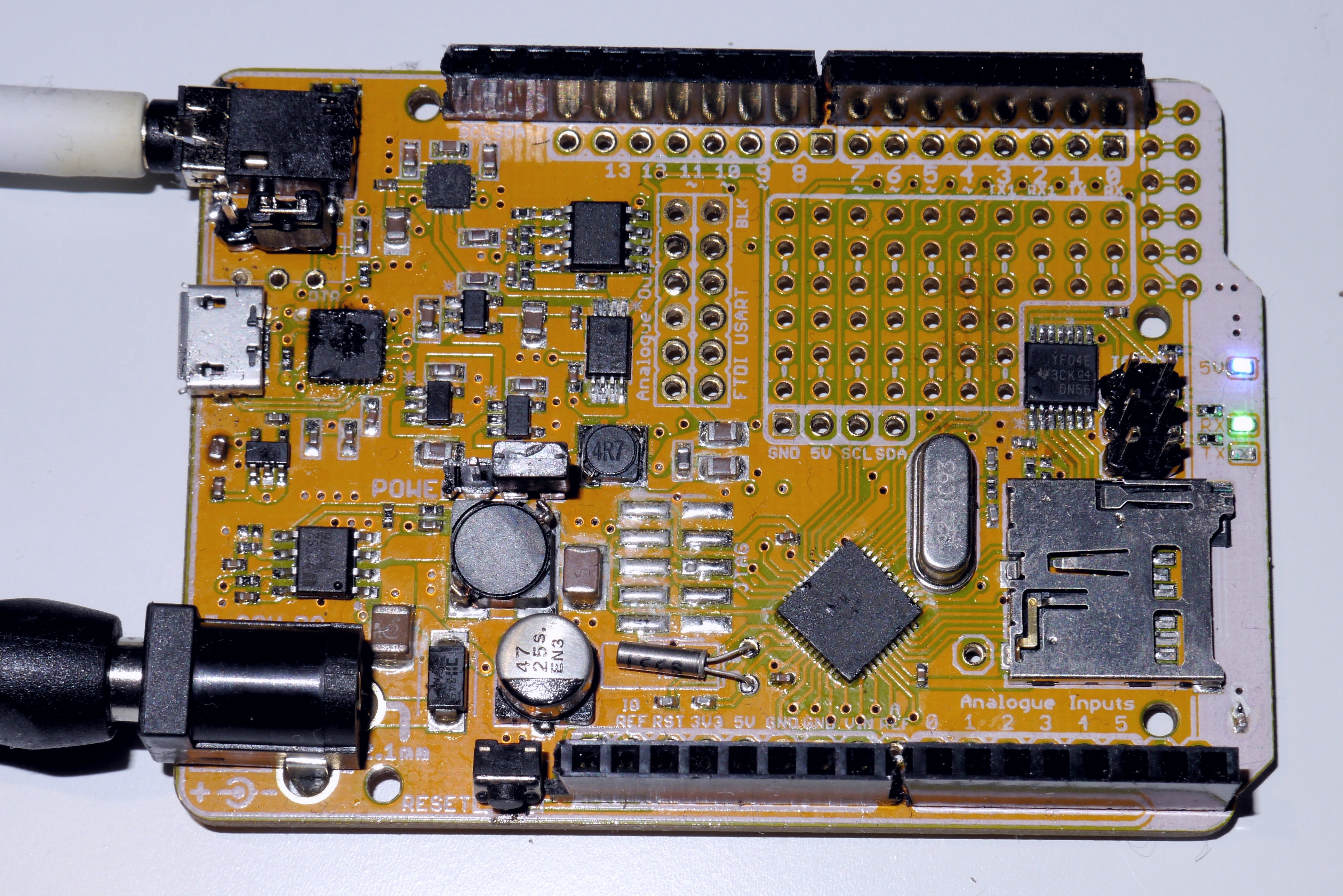
Goldilocks Analogue – Prototype 2
Now that the new prototype for the Goldilocks Analogue is completed, it is time to test it to see how successful the design was. And interestingly, in the time that I’ve been designing the Goldilocks Analogue, Stanford University in collaboration with Texas Instruments have produced their own Analog Shield.
So this test will compare the Goldilocks Analogue with its dual channel 12bit MCP4822 DAC with the Stanford Analog Shield quad channel 16bit DAC8564 DAC. In a later test sequence, using the same test tone, I compare the Goldilocks Analogue with the Open Music Labs Audio Codec Shield using a Wolfson Micro WM8731 24 bit Codec with ADC, DAC, and signal processing capabilities.
Summary (TL;DR)
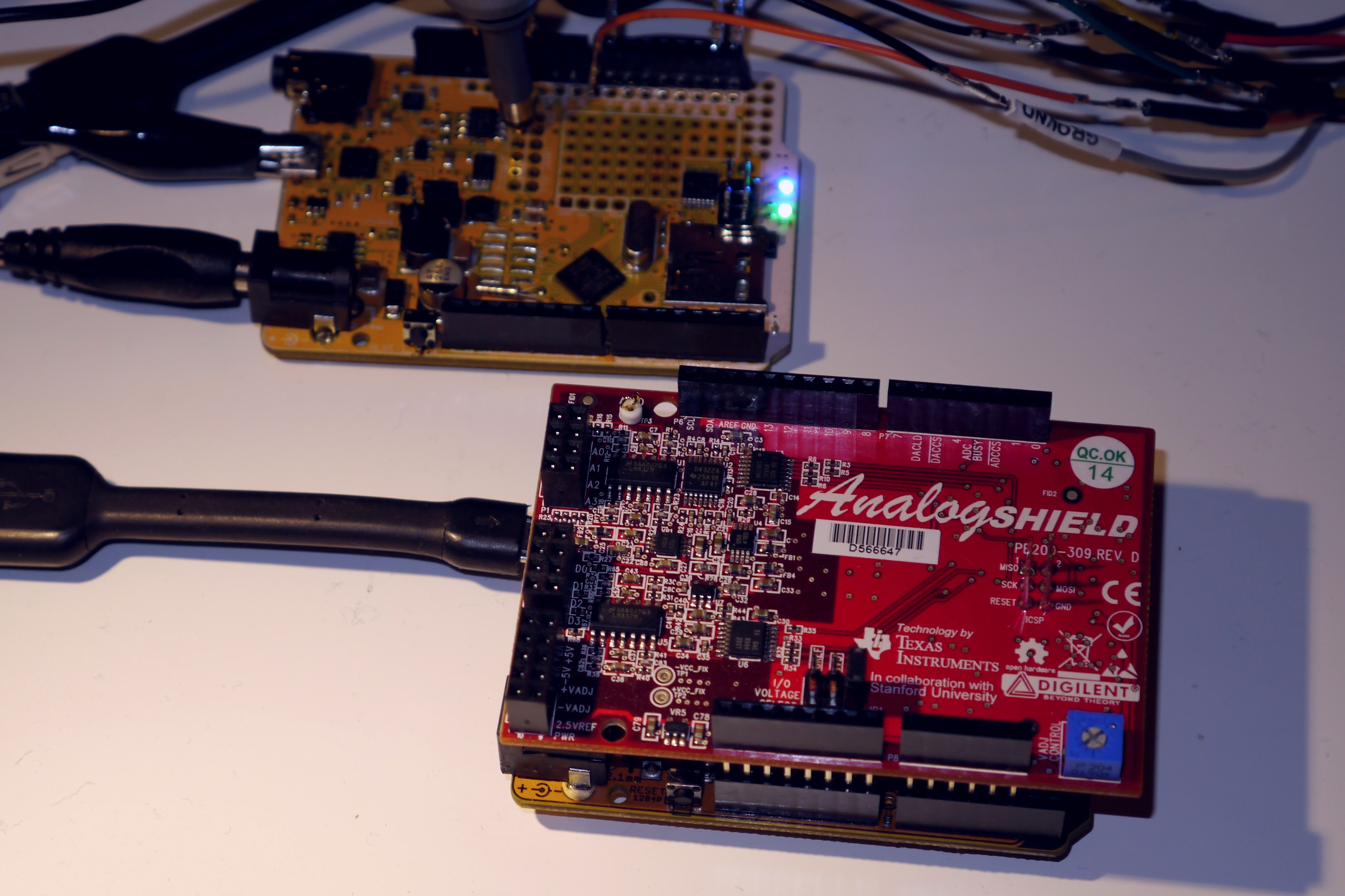
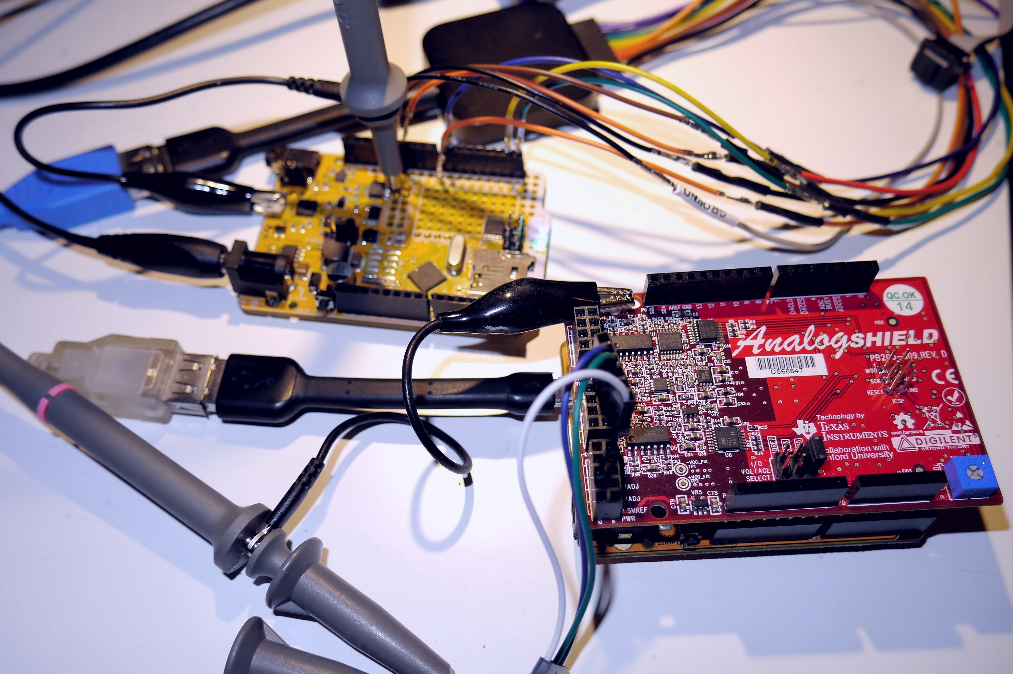
The test platform is essentially the same ATmega1284p device, clocked at 22.1184MHz. For the Goldilocks Analogue it is integrated on to the main board. For the Analog Shield I used a Goldilocks device as provided in the Pozible project.
You don’t need a lot of space to have great tools. I’m using a Red Pitaya device, configured as an oscilloscope and as a spectrum analyser, together with a Saleae Logic to capture SPI transactions.

Micro Test bench – Red Pitaya and Saleae Logic
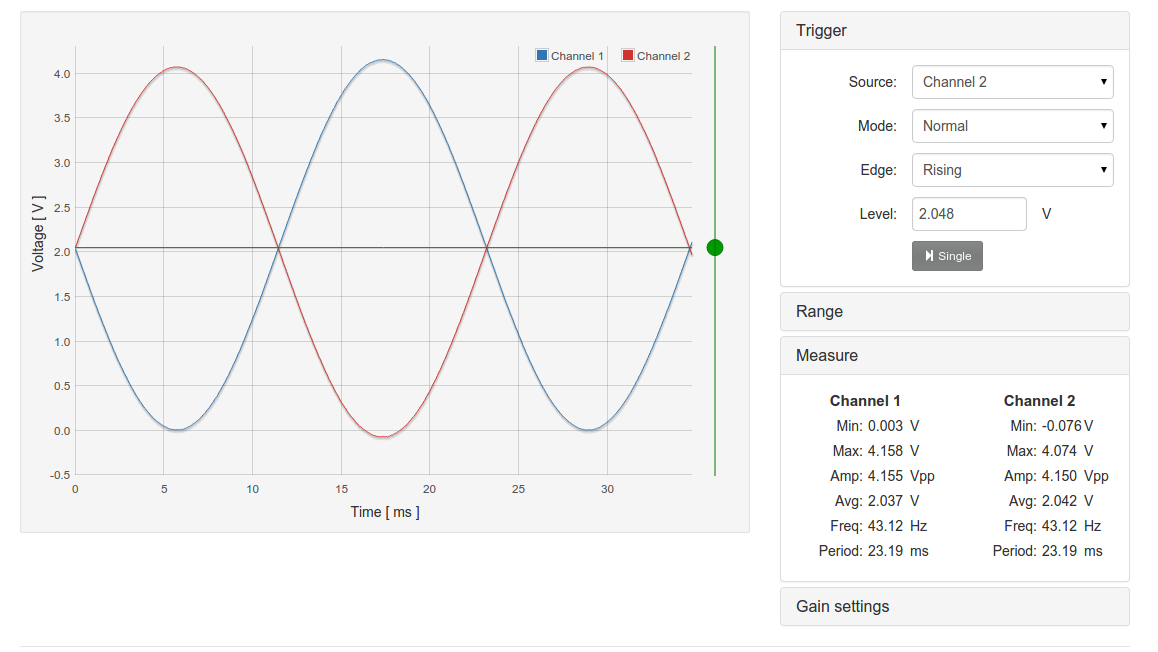
Both Goldilocks Analogue and Analog Shield are comfortably capable of producing reasonable quality stereo signals at 44.1kHz sampling rate. Both devices output beautiful looking 43.1Hz sine waves, at 44.1kHz reconstruction rate, from a 16 bit 1024 sample Sine Wave.
The Goldilocks Analogue produces 0V to 4.096V 1:1 buffered signals from its DC outputs, and an AC amplified headphone output in parallel. The Analog Shield produces -5V to +5V balanced amplified signals from the 0 to 2.5V DAC.

Full Swing 43.1Hz Sine Wave Goldilocks Analogue – Blue 0V to +4.096V Analog Shield – Red -5v to +5V
The Analog Shield shows a lot of harmonics at high frequencies as shown. Comparing the two solutions, the Analog Shield doesn’t do justice to the extra 4 bits (theoretically 98dB SNR 16 bit DAC), over the Goldilocks Analogue (theoretically 74dB SNR 12 bit DAC). The BOM price difference between MCP4822 ($4.60) and DAC8564 ($20) is hard to justify given the performance demonstrated.
I think that using the platform of the AVR ATmega (Arduino) there is little point using a 16 bit DAC. There is too much noise (many mV) in the power supply and around Goldilocks or Arduino Uno or Mega boards to make more than 10 to 12 bits of DAC resolution (or ADC resolution) in any way relevant.
Overlaid 976kHz Spectrum – Analog Shield Red – Shows significant harmonics
Stanford – TI Analog Shield
As part of its microcontroller course, Stanford University required a platform to sample and generate analogue signals. The Standford – TI Analog Shield arose from this need.
The Analog Shield contains a Texas Instrument quad channel ADC and a quad channel DAC, together with a variable voltage supply. I have not tested the ADC.
The DAC capability is based on a Texas Instrument DAC8564 device. This device has many interesting features, including the ability to synchronise loading of updated digital outputs, and to maintain multiple power-down states. The DAC8564 has many great features, and it comes with a price tag to match its capabilities.
Analog Shield – Quad 16bit DAC & Quad 16bit ADC – Stanford University & Texas Instruments
Signals generated by the DAC8564 (from 0v to 2.5V) are biased around 0V and amplified to produce a 10V full swing output. The output exhibits some “cramping” around 0x0000 (-5V) outputs.

Analog Shield – Quad DAC Schematic – -5V to +5V full swing
Head to Head
Testing was done using a 16 bit 1024 sample Sine Wave file. Outputs were generated by a timer triggered to interrupt every 22.7us (44.1kHz), and produce a new output level. Testing should show only a main signal at 43.1Hz, and the reproduction frequency of 44.1kHz. The Goldilocks Analogue discards the lower 4 bits of the samples and only outputs the 12 most significant bits.
Theoretically, the Goldilocks Analogue MCP4822 DAC should be able to achieve 74dB SNR, with its 12 bits of resolution, based on the rule of thumb SINAD = (6.02 x BITS) + 1.76. For the Analog Shield DAC8564 the number is 98db SNR.
Head to Head Testing – Using Red Pitaya and Saleae Logic
All outputs generated by a 1024 sample 16bit Sine wave, generated with a 44.1kHz reconstruction sample rate, triggered by an interrupt timer.
Goldilocks Analogue – 43Hz Sine Wave – Two Channels – One Channel Inverted

Analog Shield – 43Hz Sine Wave – Two Channels – One Channel Inverted
In previous testing on the Goldilocks Analogue prototype I had found that my OpAmp devices were unable to achieve 0V properly. In this new prototype I have produced a stable -1.186V Vss supply for the OpAmp. The signals at 0x000 show that I’ve achieved the required result, with the output being smooth down to the 0x000 level, and up to 0xFFF as well.
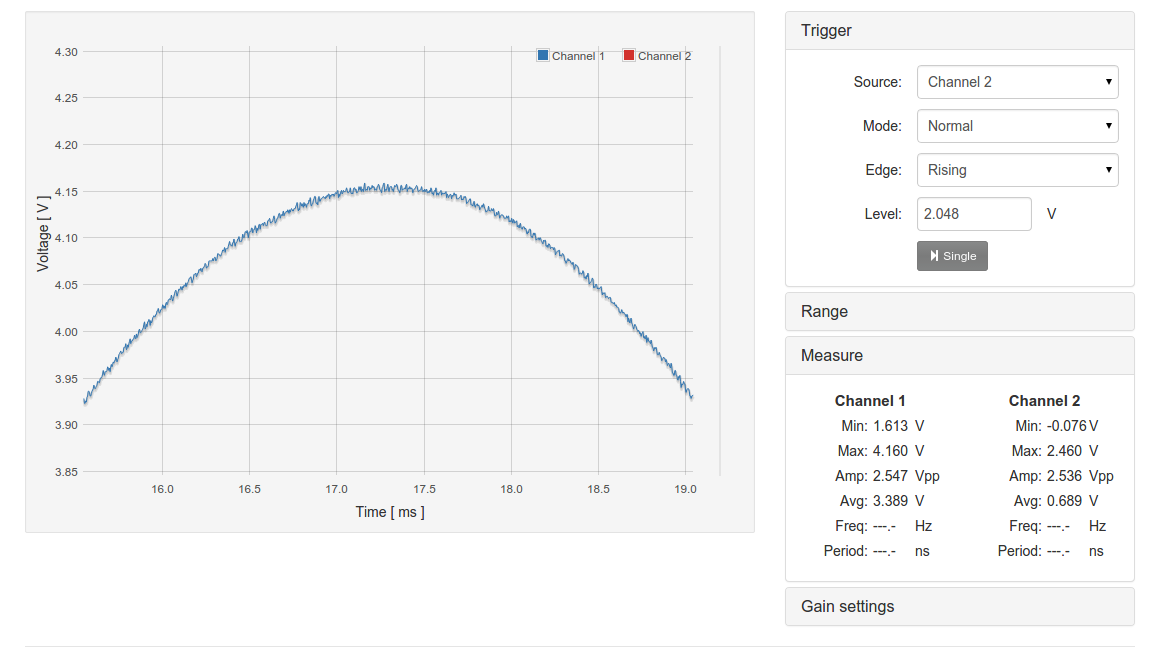
Goldilocks Analogue – 0xFFF Output
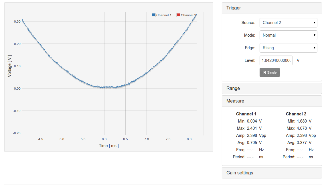
Goldilocks Analogue – 0x000 Output
The Analog Shield also produces smooth signals, but it does display some compression around 0x0000 levels. Possibly because of some issues with generating the Vss rail for the OpAmps.

Analog Shield – 0xFFFF Output
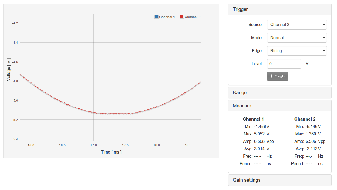
Analog Shield – 0x0000 Output – Slight Clipping
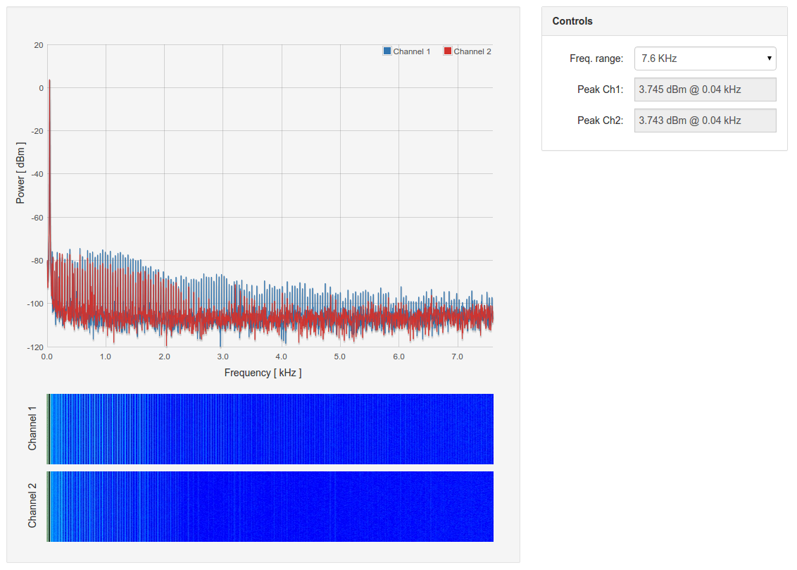
Looking at the spectra generated by both implementations up to 953Hz it is possible to see harmonics from the Sine Wave, and other low frequency noise.
The spectra are not directly comparable, because the Goldilocks Analogue is producing a 4V full swing, or -4dBm, whilst the Analog Shield is producing a 10V full swing, or 3.7dBm. Distortions in the Analog Shield need to be reduced by 7.7dB to be equivalent to distortion in the Goldilocks Analogue.
The spectrum produced by the Goldilocks Analogue shows most distortion is below -70dB, and that the noise floor lies below -100dB.

Goldilocks Analogue – 43.1Hz Sine Wave – 953Hz Spectrum
The Analog Shield has a significant noise present at 50Hz, which may be caused by noise leakage through the PC USB power supply not being completely filtered before the supply is provided to the DAC8564. Other noise rises above -80dB, and is present right across the spectrum.

Analog Shield – 43.1Hz Sine Wave – 953Hz Spectrum
In the spectra out to 7.6kHz we are looking at the clearly audible range, which is the main use case for the devices.
The Goldilocks Analogue has noise carriers out to around 4.5kHz, but they are all below -80dB. After 4.5kHz the only noise remains below -100dB.
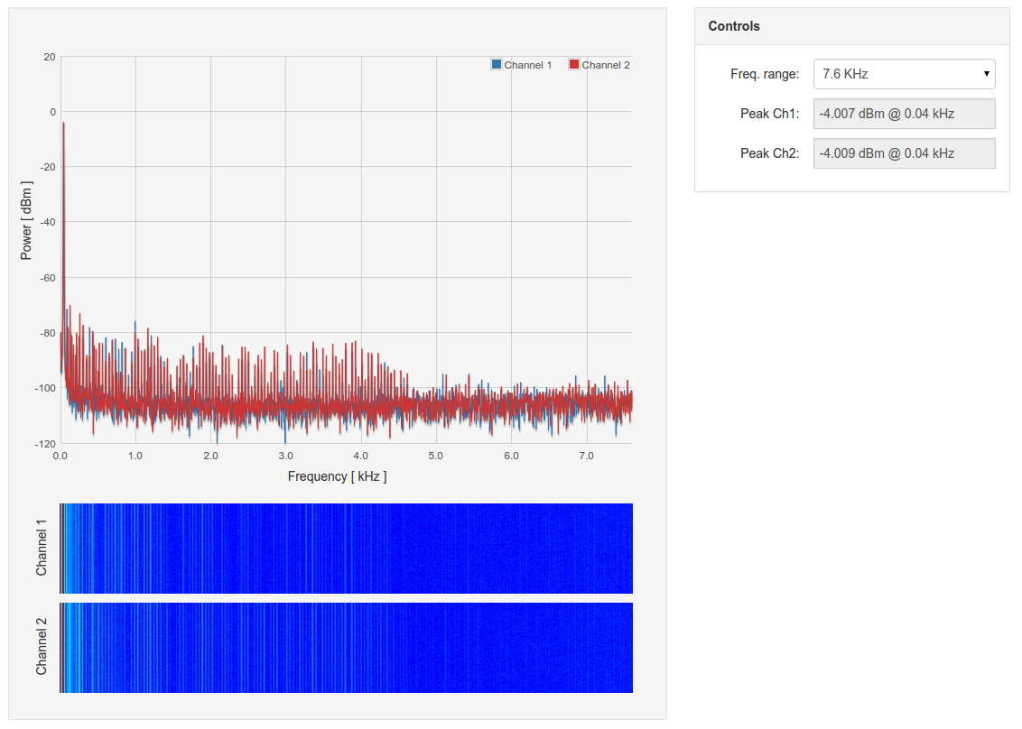
Goldilocks Analogue – 43.1Hz Sine Wave – 7.6kHz Spectrum
The Analog Shield shows noise carriers out to only 2.5kHz, but on one channel these are above -80dB. Otherwise the test shows mainly background noise below -100dB beyond 2.5kHz.
Analog Shield – 43.1Hz Sine Wave – 7.6kHz Spectrum
The spectra out to 61kHz should show a noise carrier generated by the reconstruction frequency of 44.1kHz.
The Goldilocks Analogue shows the spectrum maintains is low noise level below -90dB right out to the end of the audible range, and further out to the reconstruction carrier at 44.1kHz.

Goldilocks Analogue – 43.1Hz Sine Wave – 61kHz Spectrum
Similarly, the Analog Shield is quiet out beyond the audible range. It exhibits a strong noise carrier at the reconstruction frequency. Also, it shows some beat frequencies generated by a small noise carrier at 10kHz, and the reconstruction carrier. These noise carriers might be caused by the TPS61093 boost power supply used to generate the +ve and -ve supplies for the output buffer OpAmps, although it has a characteristic frequency at 1.2MHz, or it might be leakage from some other device.

Analog Shield – 43.1Hz Sine Wave – 61kHz Spectrum – Harmonics around 44.1kHz reconstruction frequency
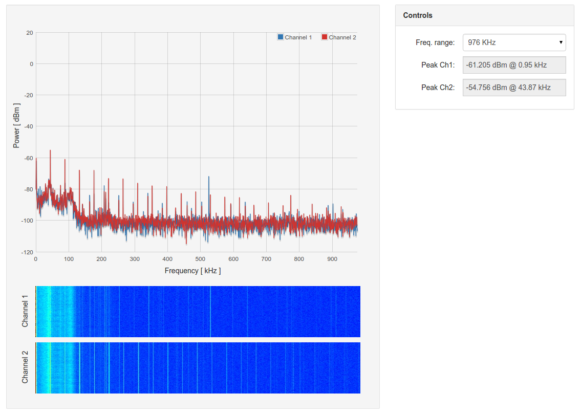
The final two spectra show the signal out to 976kHz. We’d normally expect to simply see the noise floor, beyond the 44.1kHz reconstruction carrier noise.
The Goldilocks Analogue has a noise carrier at around 210kHz. This could be generated by one or both of the TPS60403 devices used to generate the negative AVss supply. These devices have a typical switching frequency of 250kHz, specified between 150kHz and 300kHz, so this is possible. Aside from the single carrier mentioned, there is no further noise out to 976kHz.
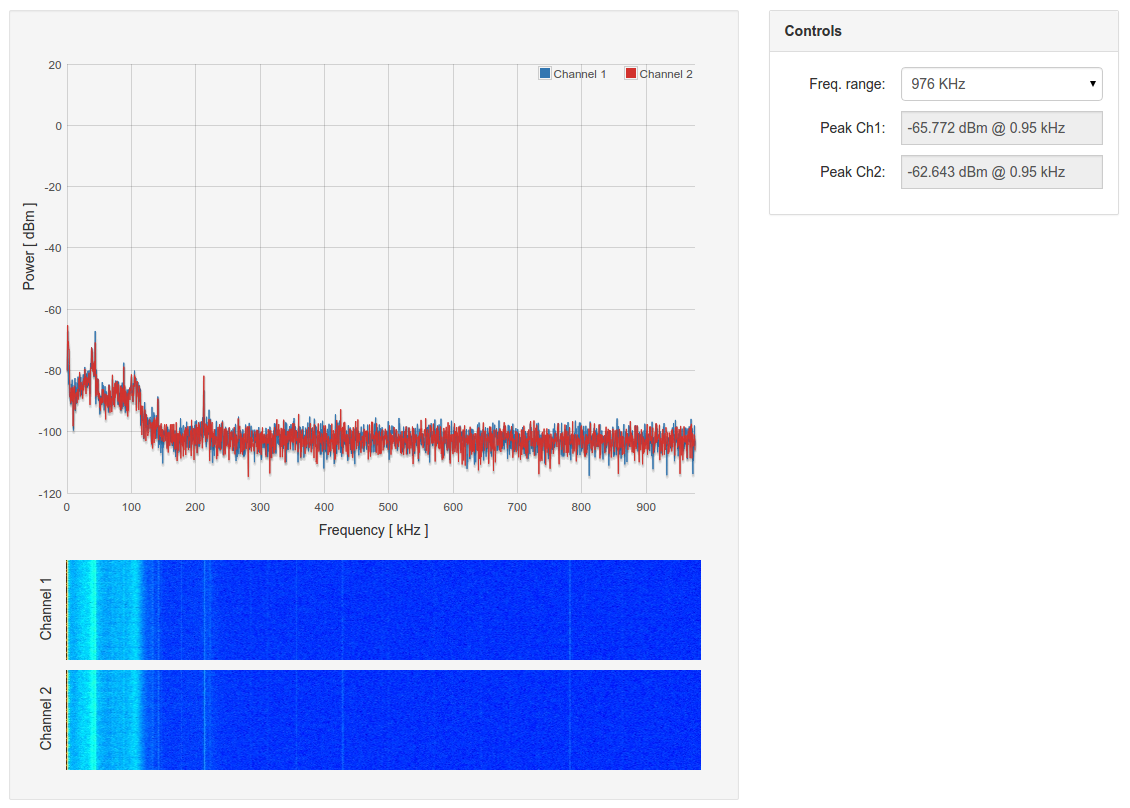
Goldilocks Analogue – 43.1Hz Sine Wave – 976kHz Spectrum
The Analog Shield shows the reconstruction carrier noise at -50dB, and then harmonics of this carrier all the way out to 976kHz. Not sure why these artifacts are appearing. There is a chance that noise derived from these signals is impacting the overall outcome for the DAC8564.

Analog Shield – 43.1Hz Sine Wave – 976kHz Spectrum
Using the Saleae Logic we can capture the SPI transactions generating the analogue result. To maintain the 44.1kHz reconstruction rate a set of samples needs to be transferred every 22.7us.
In the code I’ve used to generate the signal an interrupt timer triggers every 22.7us indicated by the rising edge of “Channel 6”. Once the interrupt has finished processing it lowers the Channel 6 line, indicating that control has returned to the main program. If required the main program has to use the remaining time to generate the required signal. Clearly the faster the SPI transaction to set up the transaction can be completed the more time available for other purposes.
The MCP4822 found in the Goldilocks Analogue has 4 control bits and 12 data bits, which are transferred in 2 8 bit transactions. To set two channels only 4 SPI transactions are required, taking 7.25us.

Goldilocks Analog SPI transaction – Interrupt duration 7.25us
The DAC8564 used in the Analog Shield has 8 control bits and 16 data bits, which are transferred in 3 8 bit transactions, or 24 SPI clock cycles. For two channels this takes 6 SPI transactions and 9.08us.
Both devices leave sufficient time for calculation of simple VCO, or other multiply based, effects in real time with 44.1kHz dual channel. Halving the sample rate to 22.05kHz would be necessary to provide more opportunity to retrieve data from uSD cards or other more complex data sources.
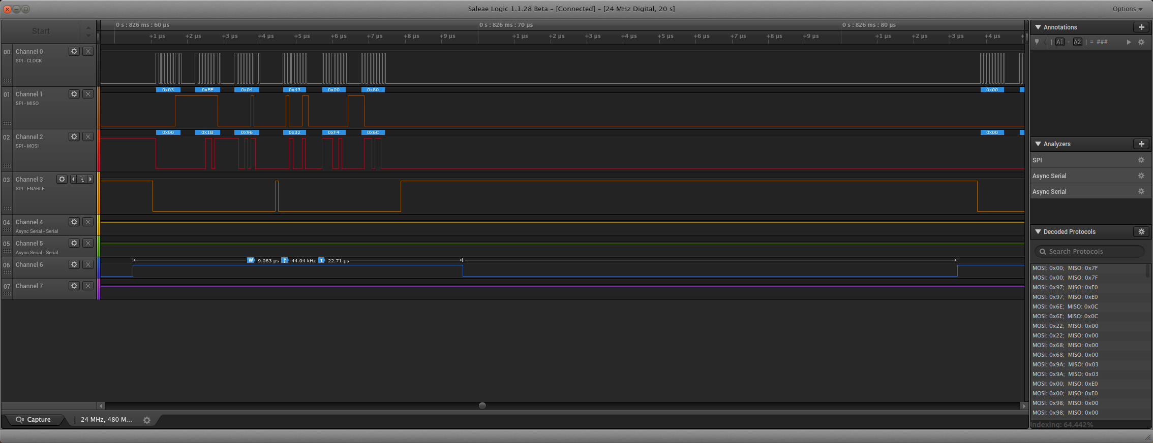
Analog Shield SPI Transaction – Interrupt duration 9.083us
The final reality check in this Head-to-Head comparison is provided by Digikey. I must say that some of the features of the DAC8564 had convinced me to look at migrating the production Goldilocks Analogue to use this new TI DAC. However, seeing that the BOM cost for the TI DAC is approximately 4 times greater than the MCP4822 device soon cooled those thoughts.
Given the cost sensitive nature of the Arduino environment it is not practical to use a device costing nearly US$20 on the Goldilocks Analogue platform, irrespective of its performance.
And, given that the Analog Shield provides no justification in terms of signal quality over the existing Goldilocks Analogue solution there seems to be no technical merit in changing the DAC specification, either.
The Microchip MCP4822 is available from US$4.60 at Digikey.

Digikey MCP4822 Pricing
The Texas Instrument DAC8564 is available from US$18.60 at Digikey.
Digikey DAC8464 Pricing
Design Review
The remaining features and functions of the Goldilocks Analogue have been tested, and resulting from these tests I’m going to make the following redesigns and changes.
- Revert to tri-state buffers for uSD I/O logic conversion CMOS 5v to CMOS 3v3 – Bi-directional translators pure fail! I tried both TI TXB and TXS devices and they simply didn’t work as specified.
- Remove USART pin-out – unnecessary feature and just takes board space.
- Move DAC pin-out to right hand edge of the prototyping space – easier to use if not covered by UNO format shield. As the Goldilocks Analogue is slightly longer than standard Arduino UNO shields, putting the DAC DC output pins outside the shield outline on the right hand end of the board will allow easier access for connections.
- Increase prototyping space – fill in space freed by pin-out removals.
- Use smaller packages where possible – heading for production.
- Increase bypass capacitors on uSD 3V supply – uSD cards consume significant current, potential for instability because of long 3V3 supply
- Use a JTAG pin for MCP4822 LDAC – to enable synchronization of the DAC channels.

Pingback: Goldilocks Analogue – Testing 3 | feilipu