Recap
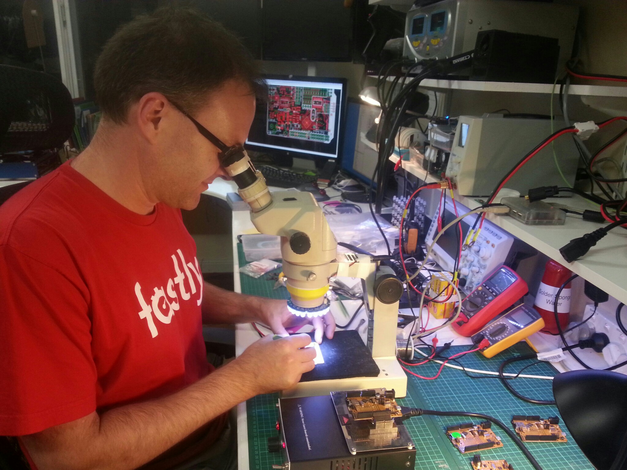
I’ve been working on the Goldilocks Analogue now for so long that its been the centerpiece of my coding evenings for the past 18 months. This is the first time that I’ve designed a piece of hardware, and I’ve managed to make many mistakes (or learnings) along the way, so I think that every step of the process has been worthwhile.
Goldilocks Analogue Prototype 4 – Rotating
In this project, I’ve learned about Digital to Analogue Converters, Operational Amplifiers, Voltage translation, Switching Power Supplies, and most importantly have gained a working knowledge of the Eagle PCB design tools.
Version History
The original Goldilocks Project was specifically about getting the ATmega1284p MCU onto a format equivalent to the Arduino Uno R3. The main goal was to get more SRAM and Flash memory into the same physical footprint used by traditional Arduino (pre-R3) and latest release Uno R3 shields.
The Goldilocks project achieved that goal, but the resulting ATmega platform still lacked one function that I believe is necessary; a high quality analogue capability. The world is analogue, but having an ADC capability, without having a corresponding digital-to-analogue capability, is like having a real world recorder (the ADC capability) with no means to playback and recover these real world recordings.
A major initiative of the Goldilocks is to bring an analogue capability to the Arduino platform via a DAC, so this project was called the Goldilocks Analogue. Following a Kickstarter campaign, the Goldilocks Analogue is now available on Tindie.

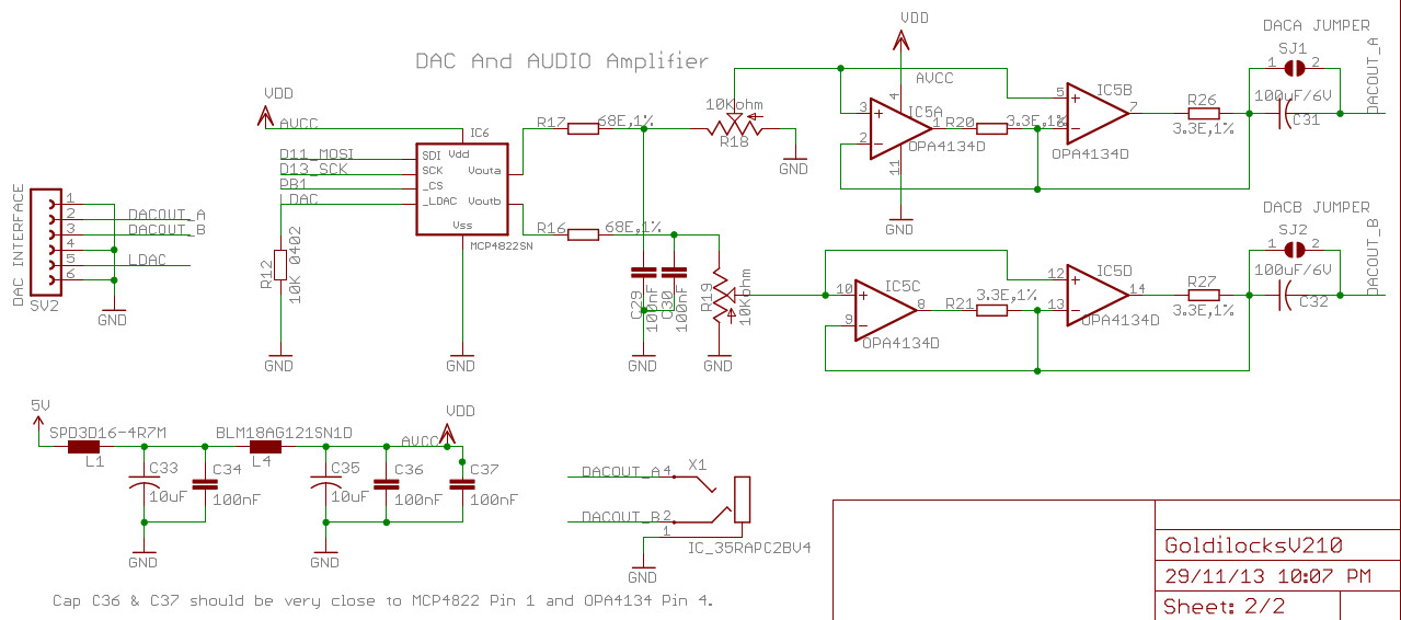
Version 1 implemented the MCP4822 DAC buffered with an expensive, very musical, Burr Brown Operational Amplifier. Although the DAC performed exactly as designed, I neglected to provide the Op Amp with a negative supply rail, so it could not approach 0V required to reproduce the full range of output available (0v to 4.096V) from the DAC. That was a mistake.
Version 1 also reverted the USB to Serial interface to use a proper FTDI FT232R device from the ATmega32u2 MCU (the solution preferred now by Arduino). Using the ATmega32u2 (or ATmega16u2) to interface with anything not running at its own 16MHz CPU clock rate is broken and doesn’t work. This is because the ATmega devices don’t produce correct serial when their CPU clock is not a clean multiple of the USART required rate. I learned this the hard way with the Goldilocks Project.
Finally Version 1 implemented a buffered microSD card interface, using devices suitable to convert from 5V to 3.3V (SCK, MOSI, CS), and 3.3V to 5V (MISO) for the SPI interface. This was a correct implementation, but later I removed it because sometimes I’m really too smart for my own good.
Goldilocks Analogue – Version P1
Some significant rework of the analogue section was required for Version 2. Firstly, I decided that audio was a significant use case for the Goldilocks Analogue so it was worth while reducing the cost of the Op Amp, and sharing that expenditure with a special purpose headphone amplifier, working in parallel with the Op Amp.
The TPA6132A2 headphone amplifier was found, and implemented into the prototype. This “DirectPath” device removes the need for large output capacitors in the signal path, as it provides a zero centred output from a single supply voltage.
Version 2 also had a lesser but fully adequate TS922A Op Amp for providing DC to full rate signals, buffering the MCP4822 DAC. I had learned that Op Amps need to be provided with a negative supply rail, if they are to achieve 0V output under load.
To create a negative supply rail for the Version 2 Op Amp, I used a pair of TPS60403 voltage inverters producing -5V from the main power supply, and then fed that signal into a TPS72301 regulator configured to produce -1.186V. This design worked very well, but needed 3 devices to produce the output and also quite a lot of board space.
Finally, for Version 2, I changed the microSD voltage translation to use the TXS0104 (TXB0104) level translation products. These special purpose devices enable the bidirectional transfer of signals over voltage transitions. Normally these two device types (TXB / TXS) work very well, but somehow I couldn’t ever get either version to work properly, which caused the microSD card to never work. This exercise was a failure, and was reverted to normal buffer logic for Version 3.
Goldilocks Analogue – Version P2
Version 3 was supposed to be my final prototype prior to putting this into a crowd funding project. I made some fairly simple changes, and I was pretty happy with the outcome of Version 2 as it was.
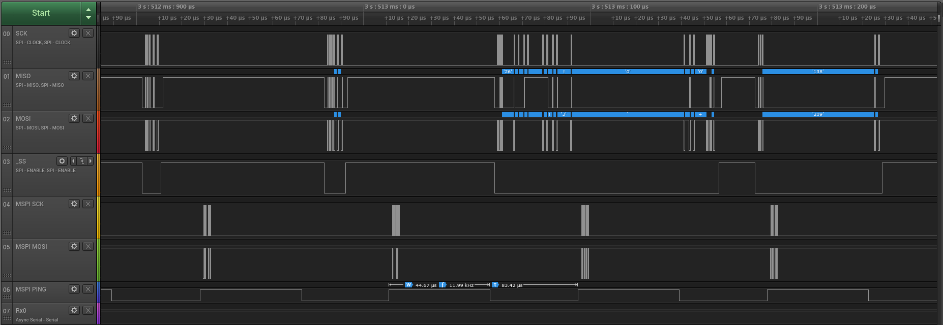
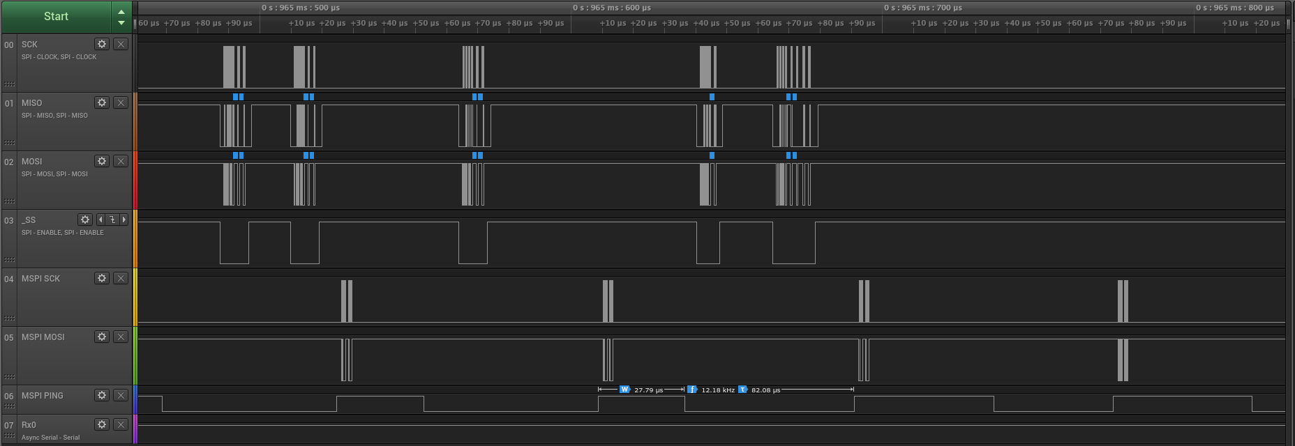
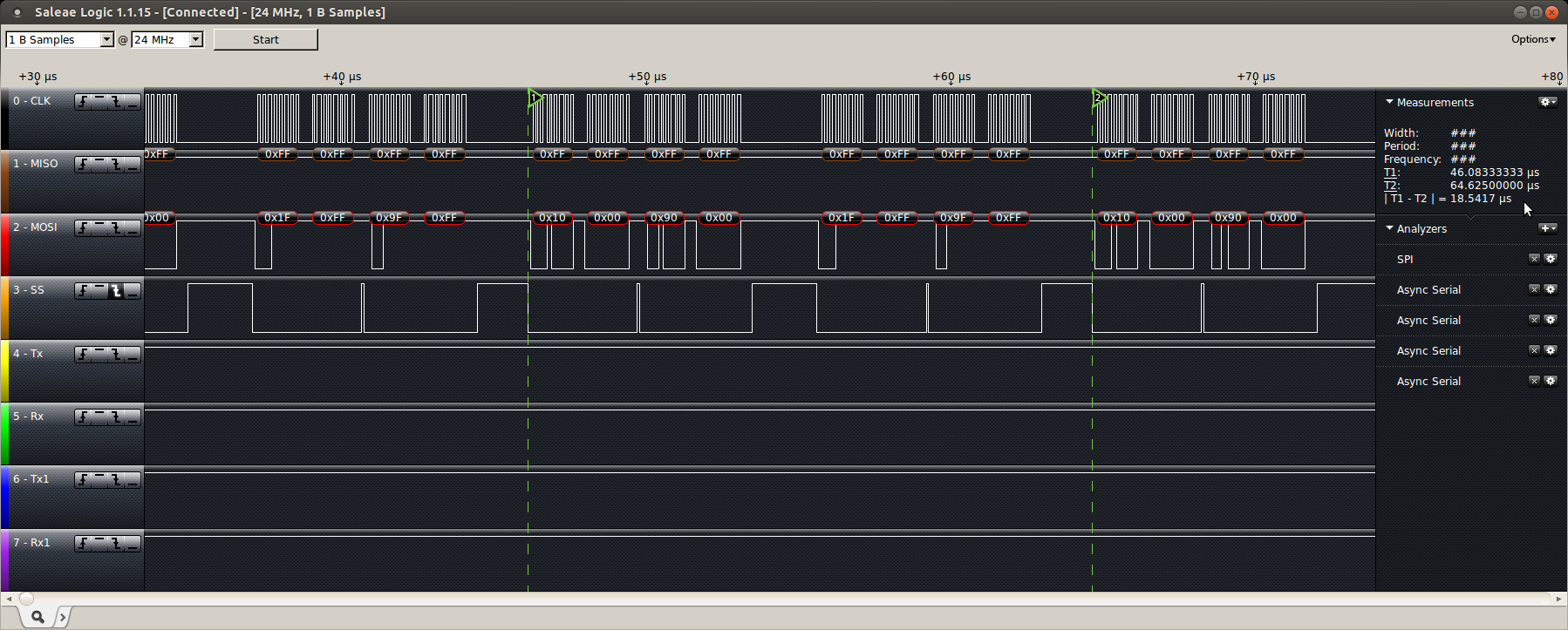
Version 3 changed the MCP4822 DAC interface to use the USART1 interface present on the ATmega1284p MCU. Using the USART1 in MSPI Mode allows the DAC to operate independently of the normal SPI bus. This frees up timing constraints on the SPI interface so that slow microSD cards can be read and streamed to the DAC, or SPI graphics interfaces can be used as in the case of the synthesiser demonstration.
As part of the testing, I found that the ATmega1284p would operate successfully at 24.576MHz. This is a magic frequency because it allows an 8 bit timer to reproduce all of the major audio sampling rates related to 48kHz. I’ve tested using this frequency and everything is working fine.
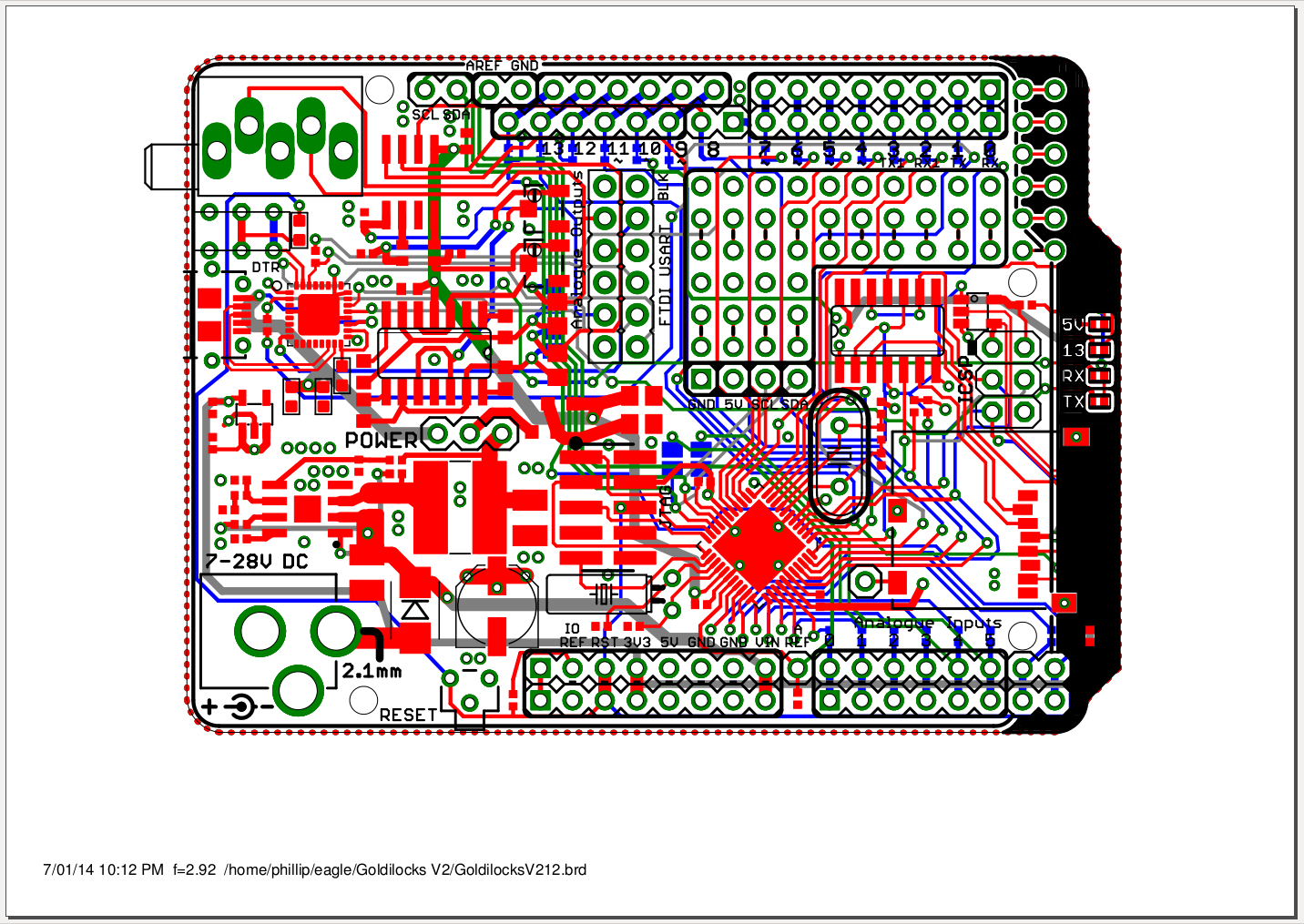
Obviously there was some feature creep over the course of experimentation, so I decided to add two SPI memory device layouts to the PCB. This would allow up to 23LC1024 256kByte of SRAM to be addressed, together with AT25M01 256kByte of EEPROM, for example. Putting these layouts on the board meant that the JTAG interface had to be moved to the back of the PCB. This was actually not a bad thing, as it would have been impossible to use the JTAG interface with a Shield in place anyway.
I was asked to beef up the 3.3V supply capability of the Goldilocks Analogue, so I added a AP1117 device capable of up to 1A supply, upgrading from 150mA.

Goldilocks Analogue – Version P3
Version 4 added the feature of amplified Microphone Input. Using the MAX9814 Mic Amp electret microphones present in the normal headsets used with smart-phones can act as an audio input to the Goldilocks Analogue. The amplified signal is presented on Pin A7, which falls outside of the normal Arduino Uno R3 footprint. For completeness, I also added a level shifted non-amplified signal (for line-in) to Pin A6.
Because of the extra microphone amplifier circuitry, I needed to reduce the footprint of the negative supply rail. So I used a regulated -3V device LTC1983 to produce the negative supply rail required for the Op Amp. There are now 3 regulators on the Goldilocks Analogue, 5V at up to 2.4A, 3.3V at up to 1A, and -3V at 100mA.
Version 4 also saw the last of the through hole components gone. Both the main crystal and the 32kHz clock crystal were reformatted into surface mount technology. This reduces the flexibility of the platform, but it makes manufacturing a bit easier.

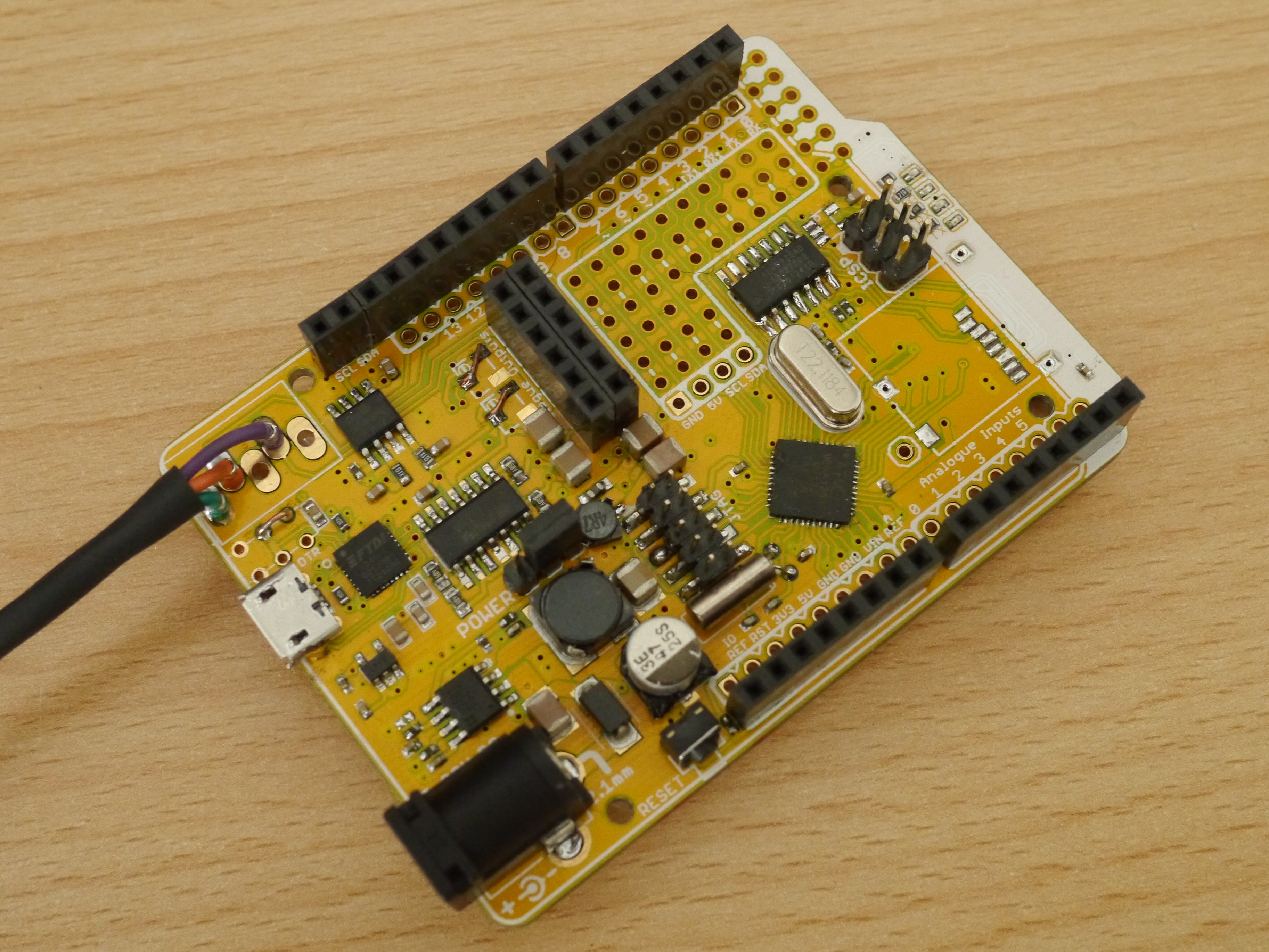
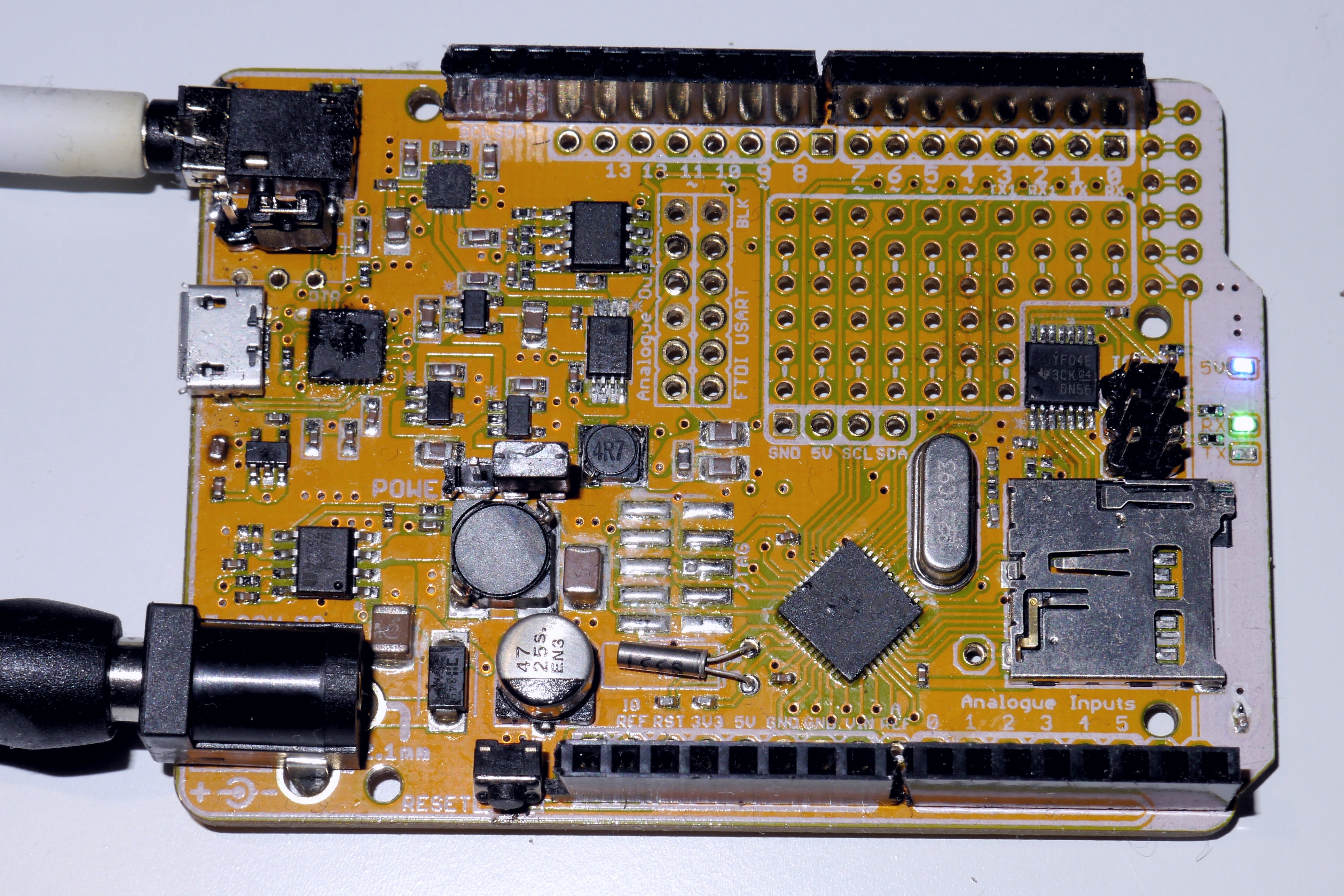
Goldilocks Analogue – Version P4
Version 4 is the end. There will be some minor adjustments to the board for the production version. But, finally, I think this is it.
Unboxing

Prototype 4 back from manufacturing
Errata
There is no power supply jumper provided. Add this to the BOM.
The EEPROM is built with SOIC8 Wide Body, but it should be Narrow Body. Fix the BOM.
Labels for the recommended power supply Voltage are partially obscured by power jack. Move the labels.
The main crystal doesn’t oscillate, because the Eagle library had an incorrect footprint.
Tested to work by rotating the crystal on its existing footprint.
Respecify the main MCU crystal to the Atmel recommended type.
Change C2 and C3 to 15pF in line with Atmel recommendation.
Change C1 and C11 to 12pF in line with Atmel recommendation.
Change R18 to 100kOhm, to bias the Analogue Line in correctly.
Add a simple LC filter to the -3.3V supply, using the known inductor and 10uF capacitor.
Tie Mic Gain to AVcc with a separable link, to produce 40dB default gain. This is the setting required for most normal microphones, so will improve the “out of box” experience for most users.
Testing

Version P4 – Front

Version P4 – Back
Power Supplies
First, looking at power supply noise, we’ve got a slightly better result for noise at the power supply over the Prototype 1. Prototype 1 used the EUP3476 Switched Mode supply device. Problems with obtaining ready supply of this device led to changing it to the AP6503, which is pin compatible but needs slightly different voltage selection resistors. In contrast to the Arduino Uno and other devices, this is very good.
We remember that 1mV represents the Voltage change in the least significant bit of the 12 bit MCP4822. The least significant bit of the ATmega1283p 10 bit ADC is about 4mV. Sampling voltages similar to the noise level inherent on the platform will not generate any further accuracy.
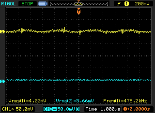
GA P4: 5V Power Supply Noise
Channel 1 (yellow) is 4.0mV of noise present at the output capacitor for the power supply, and represents the lowest noise inherent in the supply. Channel 2 (blue) is the 5.6mV supply noise present on a test pin closest to the MCU.
The significant improvement in noise level for the GA4 version at the MCU may be due to the currently decreased system clock rate, and therefore is subject to confirmation.
GA P1: 5V Power Supply Noise
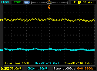
Checking the other power supplies on the board, Channel 1 (yellow) is the 3.3V positive supply, provided by a linear regulator. This supply is not used for analogue components, so the 4.3mV noise level is not critical.
Channel 2 (blue) below shows the -3V supply for the Operational Amplifier. This shows a 10mV supply voltage ramp, generated because it is a capacitive charge switching device. This is not particularly good, and it will be worth adding an LC filter to attempt to further smooth this supply, for the production Goldilocks Analogue.

GA P4: 3.3V & -3V Power Supply Noise
Microphone Input
Microphone amplifier works.
Interestingly, when the amplifier is set to 60dB gain (default setting, Channel 2, blue) it oscillates at 144kHz when not connected to anything, while it doesn’t do this with the normal gain setting of 40dB (Channel 1, yellow) based on the amplification required for typical smartphone headphones. In either case, as soon as the Mic input is grounded, the Mic output reduces to less than 4mVAC on the correct bias of 1.25VDC.
Suggest to make 40dB amplification the default setting for the production Goldilocks Analogue, but allowing the connection to be segmented for increased amplification if required.
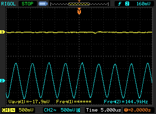
GA4 – Mic Oscillation Comparison at 40dB (CH1) and 60dB (CH2) amplification.
Line-In (PA6) seems to be biased at 1.07V rather than 1.25V. Check calculation again… Doh! R18 should be 100kOhm.
Analogue Output
The standard test that I’ve been using throughout the development is to feed in a 43.1Hz Sine wave generated from a 1024 value 16 bit LUT. The sampling rate is 44.1kHz, which is generated by Timer 1 to get the closest match.
The spectra and oscilloscope charts below can be directly compared to the testing done with previous prototype versions of the Goldilocks Analogue.
The below chart shows the sine wave generated at the output of the Op Amp. This is exactly as we would like to see, with no compression of either the 4.096V peak, or the 0V trough.

Goldilocks Analogue P4 – 43Hz Sine Wave – Two Channels – One Channel Inverted
Looking at the spectra generated up to 953Hz it is possible to see harmonics from the Sine Wave, and other low frequency noise.
The spectrum produced by the Goldilocks Analogue shows most distortion is below -70dB, and that the noise floor lies below -100dB.
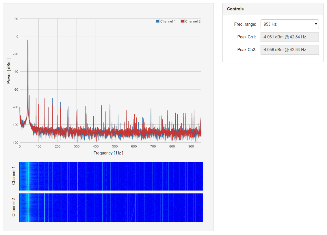
Goldilocks Analogue P4 – 43.1Hz Sine Wave – 953Hz Spectrum
Comparing the same DAC output channel A from Op Amp (Channel 1 – Blue) with the same Headphone Amp Left (Channel 2 – Red), we see slightly more noise carriers.
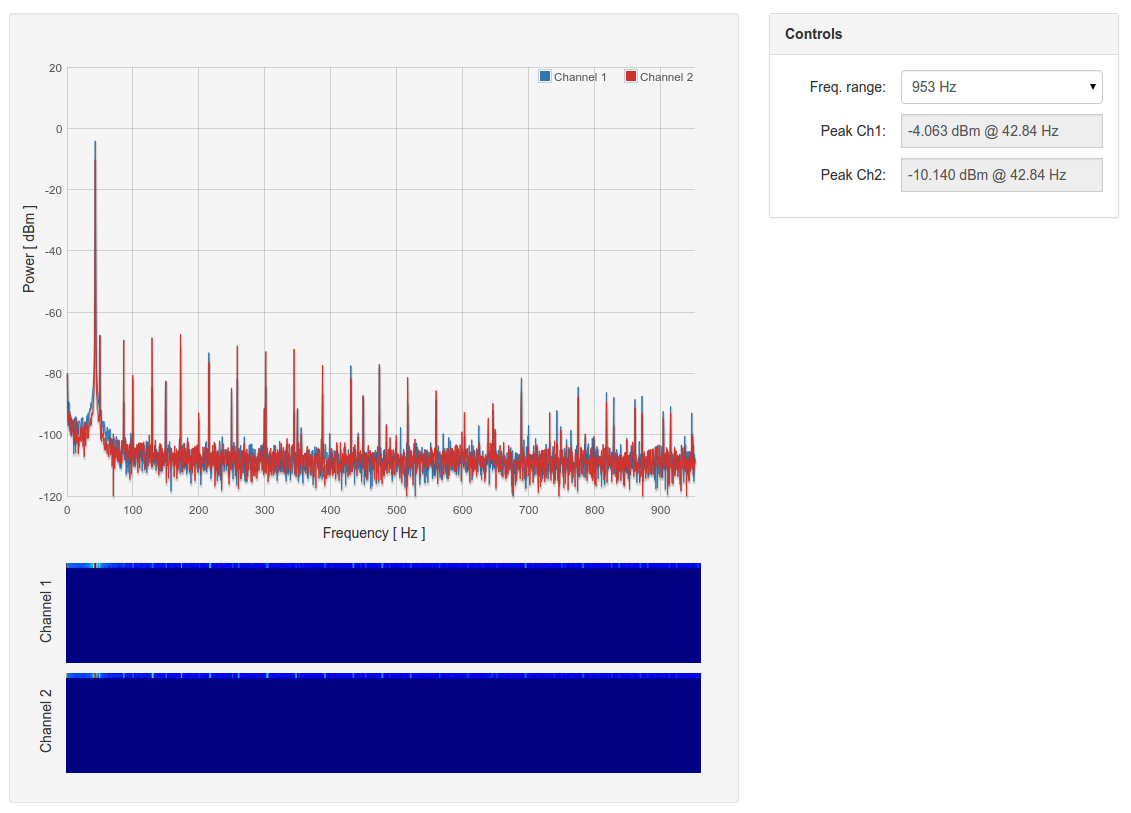
Goldilocks Analogue P4 – 43.1Hz Sine Wave – 953Hz Spectrum – Headphone in Red
In the spectrum out to 7.6kHz we are looking at the clearly audible range, which is the main use case for the device.
The Goldilocks Analogue has noise carriers out to around 4.5kHz, but they are all below -80dB. After 4.5kHz the only noise remains below -100dB.

Goldilocks Analogue P4 – 43.1Hz Sine Wave – 7.6kHz Spectrum
The spectra out to 61kHz should show a noise carrier generated by the reconstruction frequency of 44.1kHz.
The Goldilocks Analogue shows the spectrum maintains is low noise level below -90dB right out to the end of the audible range, and further out to the reconstruction carrier at 44.1kHz.
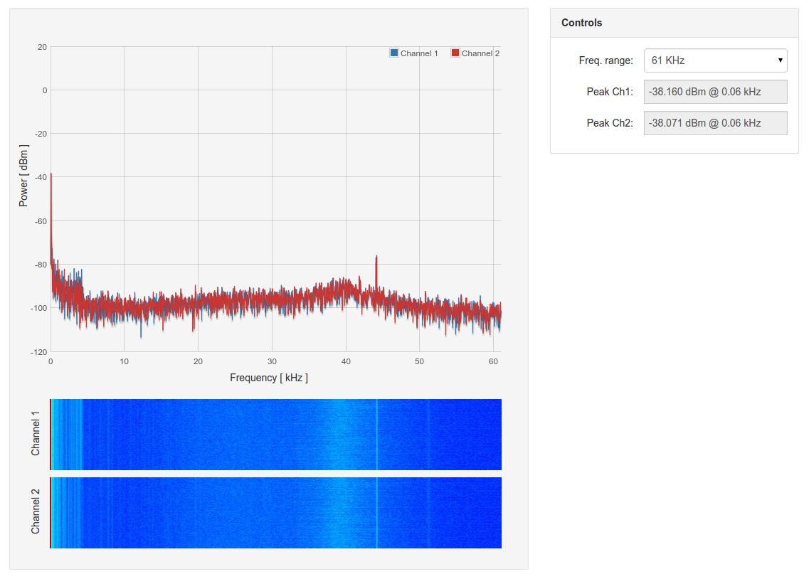
Goldilocks Analogue P4 – 43.1Hz Sine Wave – 61kHz Spectrum
The final spectrum shows the signal out to 976kHz. We’d normally expect to simply see the noise floor, beyond the 44.1kHz reconstruction carrier noise.
The Goldilocks Analogue has a noise carrier at around 210kHz. Aside from the single carrier mentioned, there is no further noise out to 976kHz.

Goldilocks Analogue P4 – 43.1Hz Sine Wave – 976kHz Spectrum
Analogue output works as specified. It can maintain the 72dB SNR required, of which it should theoretically be capable.
SPI Devices
MicroSD works.
SPI SRAM / EEPROM devices work.
Tests for REWORK
These tests are for the factory rework of the prototype boards.
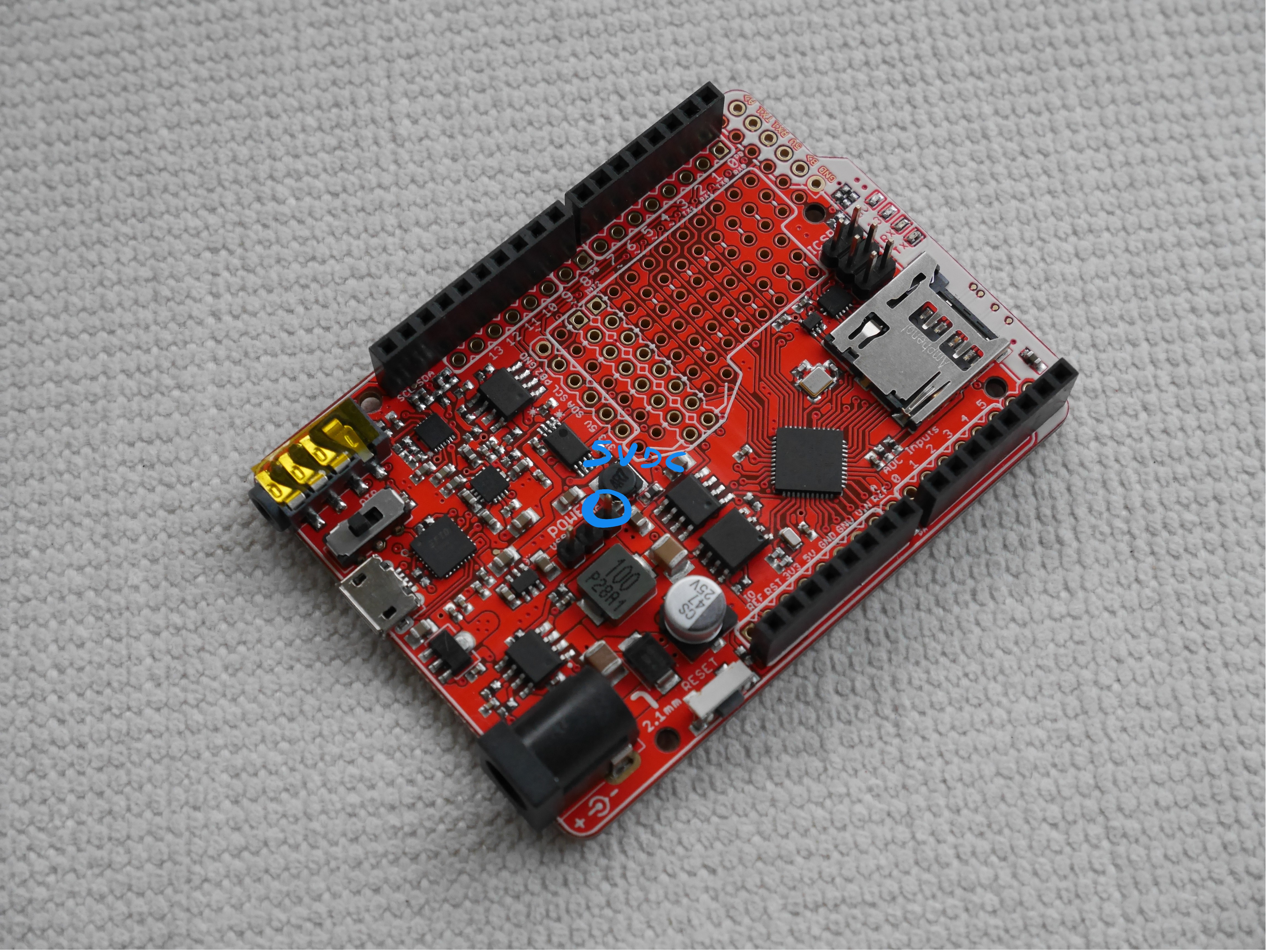
Check 5V Power Supply
Plug 7-23VDC positive centre into J1.
CHECK: that there is 5VDC available on H15 DC Pin.
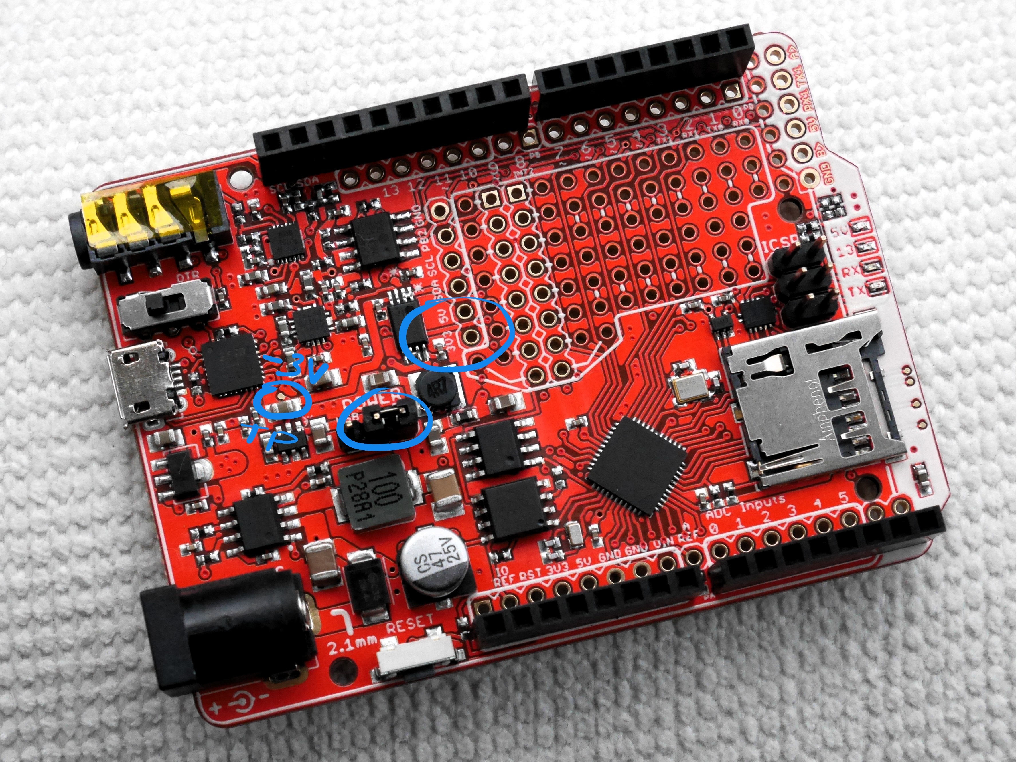
Check 3.3V and -3V Power Supply
Add a jumper to J1 from the centre pin to DC Pin.
CHECK: that 5VDC, 3.3VDC, and -3VDC is available at the test points indicated.
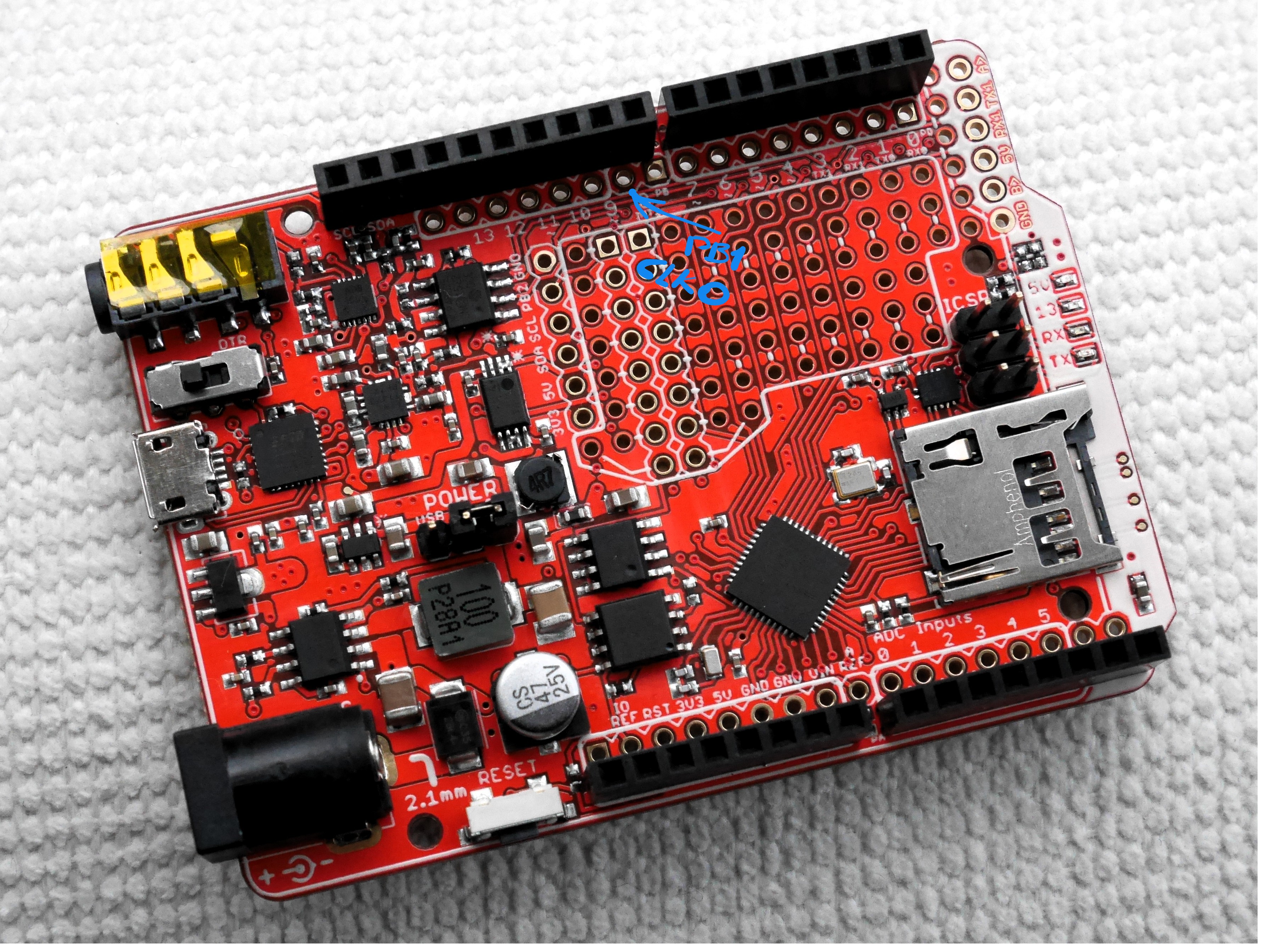
Check for Internal RC Oscillator Function
Connect an AVRISP Mk2 in circuit programmer to the ICSP Socket.
Use the following command to enable the CLKO on PB1, and set other fuses correctly.
avrdude -pm1284p -cavrisp2 -Pusb -u -Ulfuse:w:0x82:m -Uhfuse:w:0xd8:m -Uefuse:w:0xfc:m
CHECK: Using an oscilloscope or counter, check that the CLKO signal on PB1 is between 7MHz and 8.1MHz (nominal value 8MHz).
Rework 24.576MHz Crystal & Capacitors
Identify Crystal Y2, and capacitors C2 & C3 and C1 & C11.
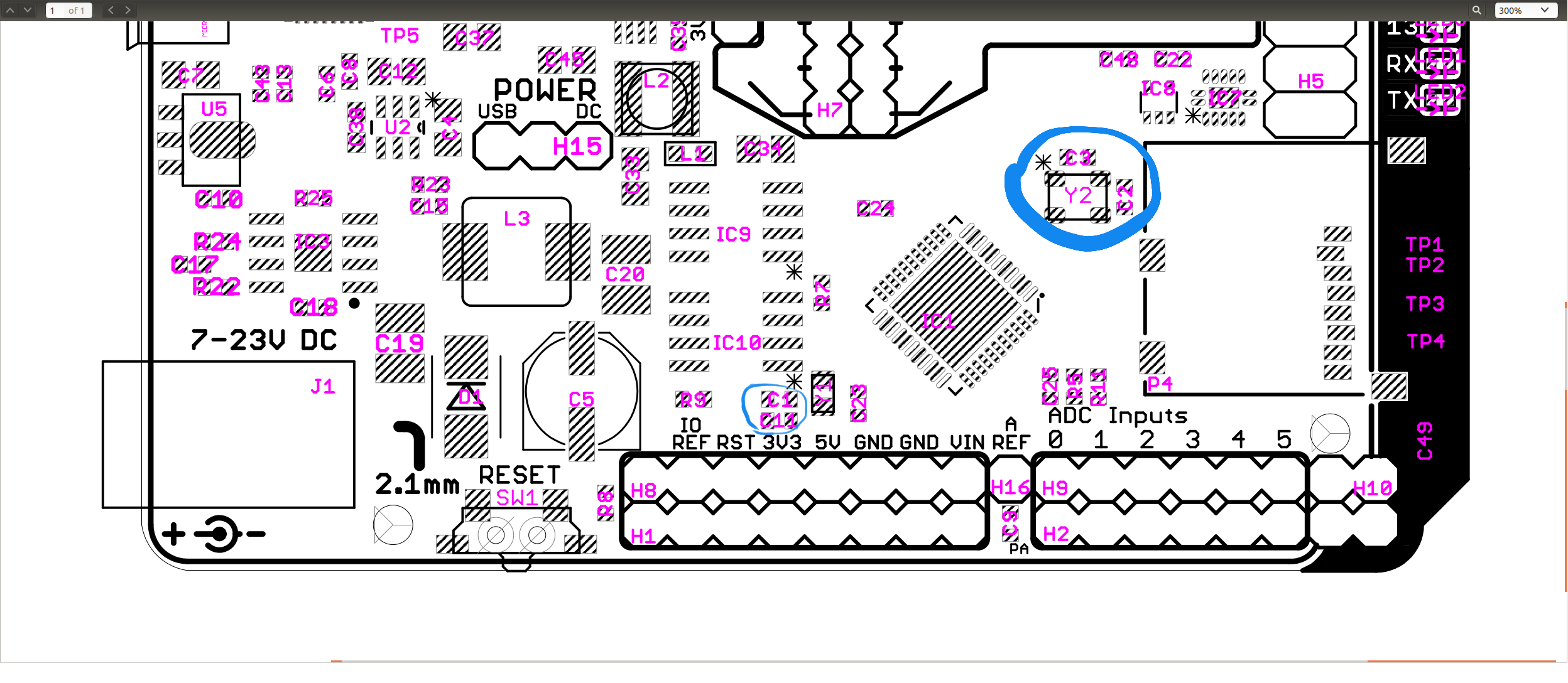
IMPORTANT: Y2 must be ROTATED 90 degrees (either direction) from standard footprint.
Rework Y2 to the 24.576MHz SMD Crystal Digikey 644-1053-1-ND device.
Rework C2 & C3 to 15pF.
Rework C1 & C11 to 12pF.
Check External Crystal Oscillator Function
Connect an AVRISP Mk2 in circuit programmer to the ICSP Socket.
Use the following command to enable the CLKO on PB1, and set other fuses to External Full Swing Oscillator with BOD.
avrdude -pm1284p -cavrisp2 -Pusb -u -Ulfuse:w:0x97:m -Uhfuse:w:0xd8:m -Uefuse:w:0xfc:m
CHECK: Using an oscilloscope or counter, check that the CLKO signal on PB1 is 24.576MHz.
Use the following command to disable the CLKO on PB1, and set other fuses to External Full Swing Oscillator with BOD.
avrdude -pm1284p -cavrisp2 -Pusb -u -Ulfuse:w:0xd7:m -Uhfuse:w:0xd8:m -Uefuse:w:0xfc:m
Rework R18
CHECK: DC voltage on Port A6 (ADC Input 6). Expected value 1.07VDC.
Identify resistor R18. R18 needs to be reworked to 100kOhm.


CHECK: DC voltage on Port A6 (ADC Input 6). Confirm the expected value 1.25VDC.
Load Bootloader
Connect an AVRISP Mk2 in circuit programmer to the ICSP Socket.
Use the following command to program a bootloader using the provided HEX file.
avrdude -pm1284p -cavrisp2 -Pusb -Uflash:w:GABootMonitor.hex:a
Connect the Goldilocks Analogue to a USB port and open a serial terminal at 38400 baud to the attached FTDI USB /dev/ttyUSB0 interface.
CHECK: Enter !!! into the serial terminal, immediately following a board RESET (using the RESET button). This will enable the Boot Monitor. These are the boot monitor commands.
Bootloader>
Bootloader>H Help
0=Zero addr (for all commands)
?=CPU stats
@=EEPROM test
B=Blink LED
E=Dump EEPROM
F=Dump FLASH
H=Help
L=List I/O Ports
Q=Quit
R=Dump RAM
V=show interrupt Vectors
Y=Port blink

Bootloader>
Bootloader>? CPU stats
Goldilocks explorer stk500v2
Compiled on = Oct  7 2015
CPU Type    = ATmega1284P
__AVR_ARCH__= 51
GCC Version = 4.8.2
AVR LibC Ver= 1.8.0
CPU ID      = 1E9705
Low fuse    = D7
High fuse   = D8
Ext fuse    = FC
Lock fuse   = FF
Close the serial terminal program (disconnect from the /dev/ttyUSB0 device).
Load Test Program
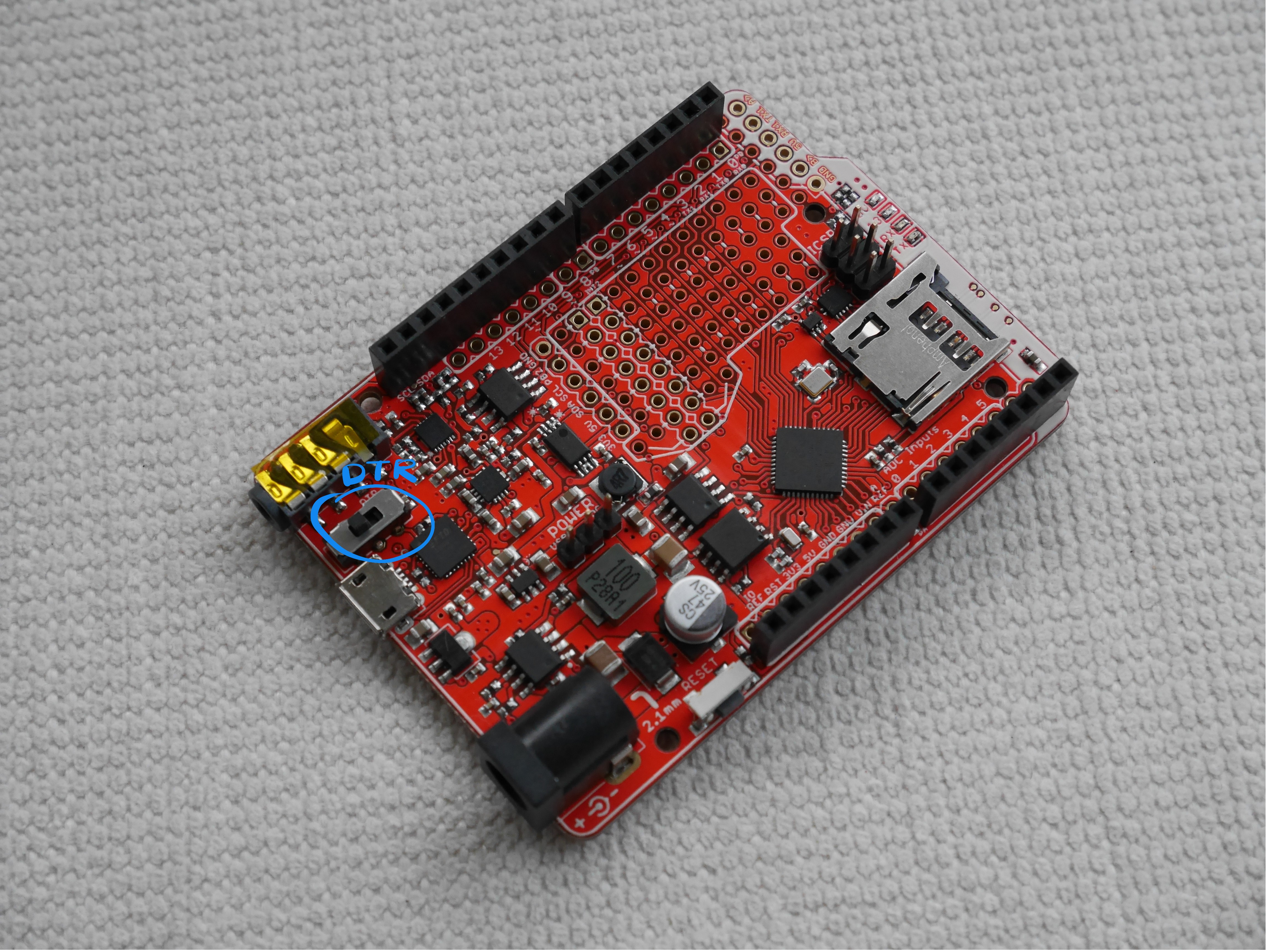
With the USB interface connected to the Goldilocks Analogue, and the DTR switch in the right most position (closest to DTR text; opposite position to the pictured position).
Use the following command to program a Test Suite using the provided HEX file.
avrdude -pm1284p -cwiring -P/dev/ttyUSB0 -b38400 -D -v -Uflash:w:GATestSuite.hex:a
Plug a standard smartphone headset (with microphone) with a 3.5mm TRRS connector in LRGM (left, right, ground, mic) configuration into the socket.
CHECK: Sound (echo of input) should be heard from the headphones, when speaking into the microphone.
Connect the Goldilocks Analogue to a USB port and open a serial terminal at 38400 baud to the attached FTDI USB /dev/ttyUSB0 interface.
CHECK: Information on each Task’s stack “Highwater” mark should be seen on the serial terminal.