The Prototype 4 has now been designed, read here for the next iteration. I’ve received the Prototype 4 back and now I’m testing them.
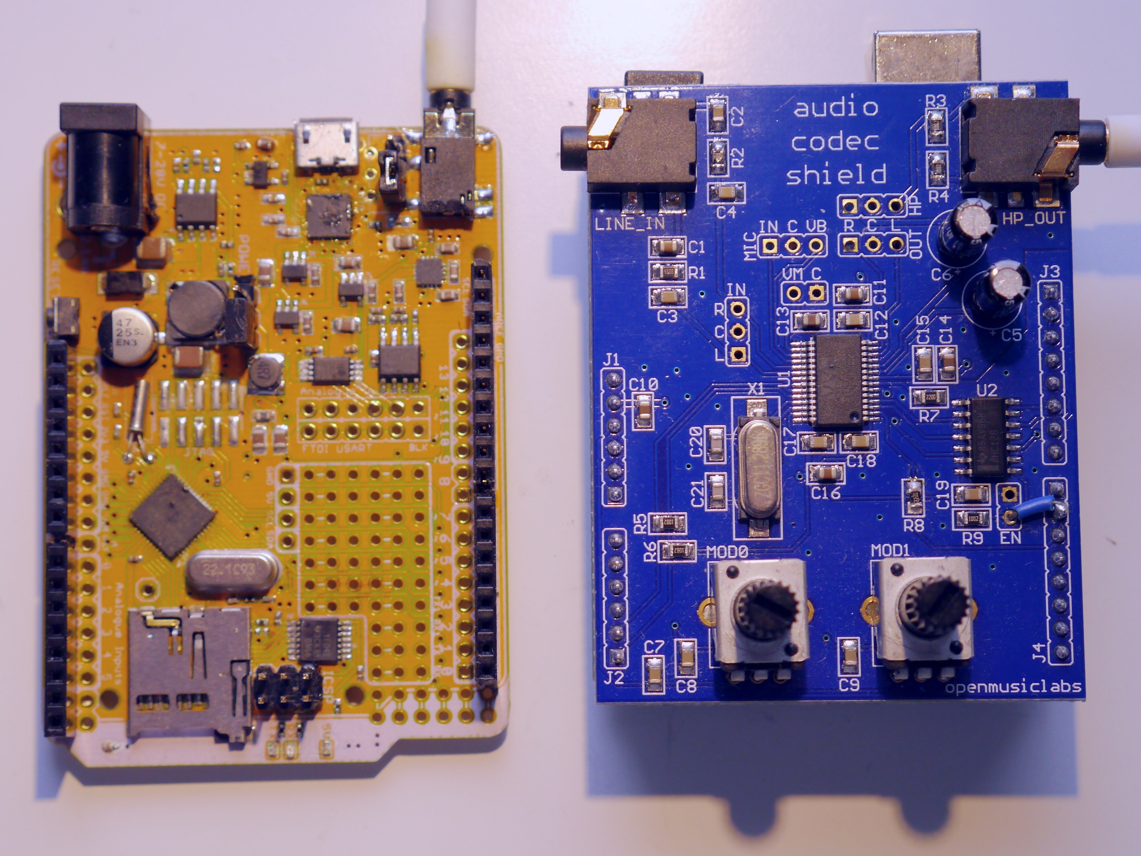
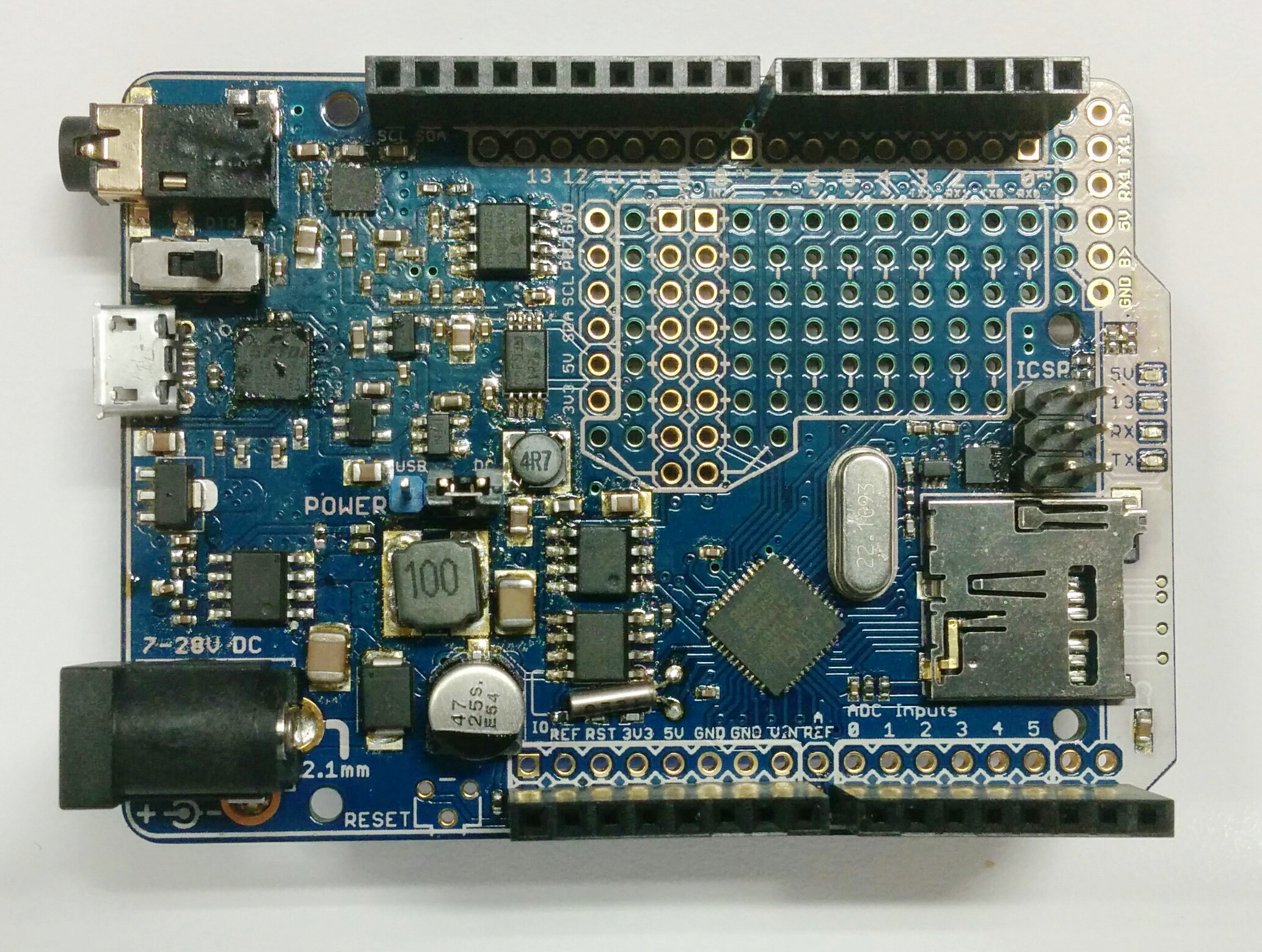
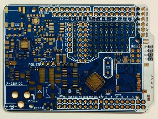
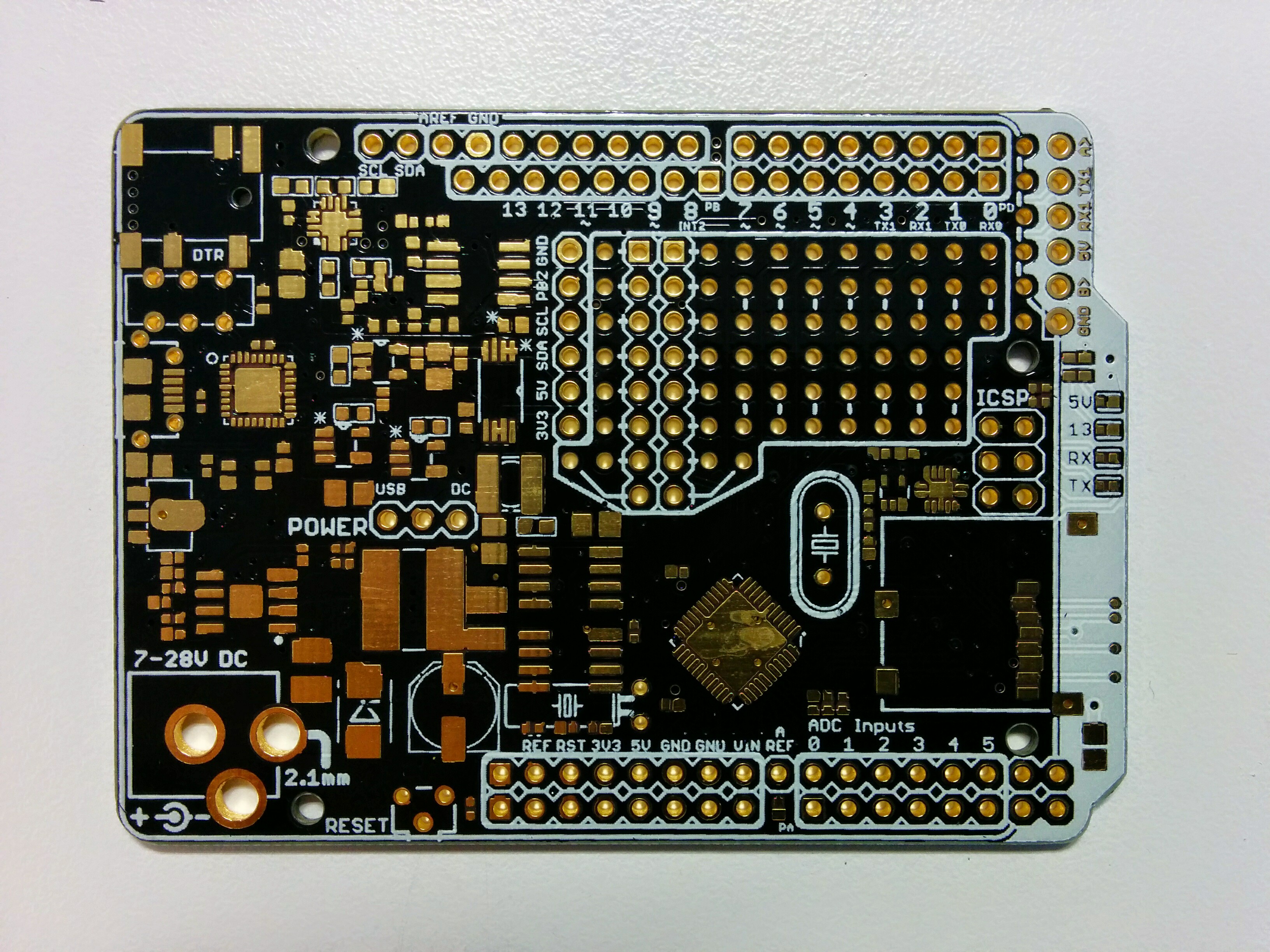
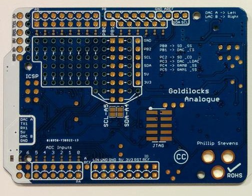
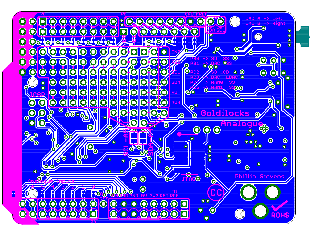
Following my initial design article, and the follow up design article, I’ve put quite a lot of thought into how I can make this Goldilocks Analogue device best achieve my stated goals. Pictured is the new 3rd Goldilocks Analogue Prototype

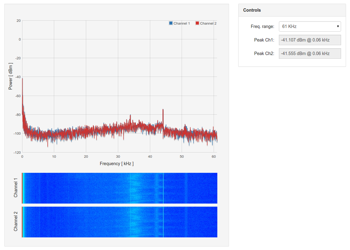
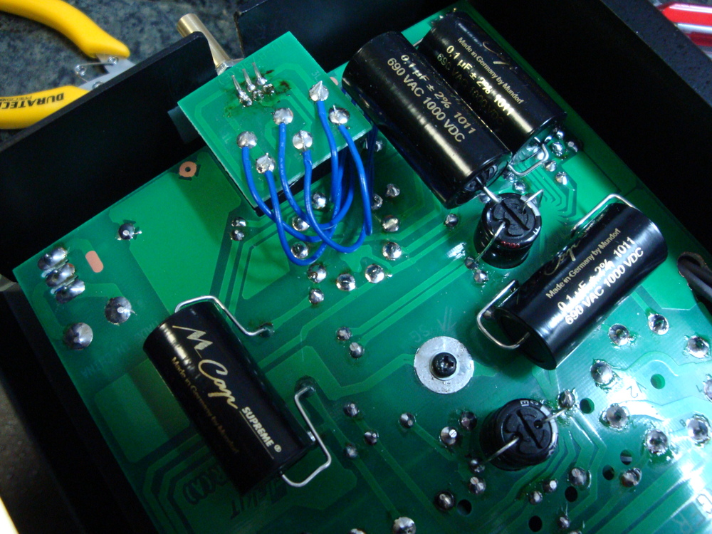
The finished prototype boards are now in my hands, and testing of the PCB configuration the new SPI EEPROM and SRAM capabilities, together with MSPIM interface for the DAC begins. These two features contribute to making the Goldilocks Analogue great analogue synthesiser platform.
Combined with a Gameduino2 LCD and touch screen, it creates flexible sound touch controller, with quality analogue output.
Goldilocks Analogue – Prototype 3
This is the working design document. It will grow as I get more stuff done, and notes added here. I’ve pretty much finished the paper design now, and will let it settle for a few weeks over the 2014 holiday season. It is sometimes good to do things again, with a few weeks perspective from the original decisions.
Goldilocks Analogue – Prototype 2
Major Revision in Strategy
Over the past months I’ve been spending time writing code to go along with the latest revision of the Goldilocks Analogue. I have successfully implemented a version of the NASA EEFS simple flash file system, to use to buffer data either for acquisition or for analogue playback, and I’ve been working on streaming functions to get data off the SD card and off the EEFS flash file system. The outcome is that it is not possible to do everything with just one SPI bus, and keep generality when needed. The SD card is just too slow, and can’t be easily interrupted. The FRAM/SRAM/EEPROM doesn’t have enough storage to effectively stream GigaBytes of data, as a uSD card can achieve.
So, what to do? Adafruit uses a software bit-banged SPI outcome to drive their MCP4921 and doesn’t get close to the maximum speed I want to achieve. Fortunately, with the ATmega1284p there is a simple answer at hand. I have decided to move the MCP4822 off the standard SPI pins, and connect it to the USART1 TX and XCK pins, using the USART in its Master SPI mode.
This is a major revision in strategy. Previously I have been very adverse to putting anything on the standards Arduino pins, preferring to keep all of the Goldilocks extra features off the Arduino footprint. However, the outcome is well worth using the USART1 to drive the MCP4822, and nothing is compromised.
USART MSPI mode is available on any ATmega device. On the UNO platform, using the ATmega328p, there is only one USART and so of course it is reserved for serial communications. The Goldilocks ATmega1284p has two USART interfaces, and usually the second one (USART 1) goes unused. Therefore connecting its XCK and TX pins to the MCP4822 is the simplest and best outcome to achieve high throughput and regularity SPI output on a non-shared SPI interface. And, as the MCP4822 DAC has high impedence (~10kOhm) inputs, having the DAC sharing the pins won’t affect normal pin usage to any extent.
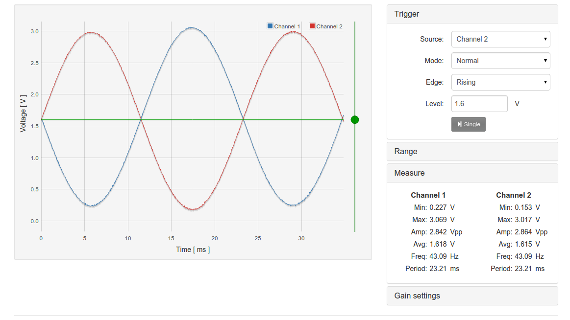
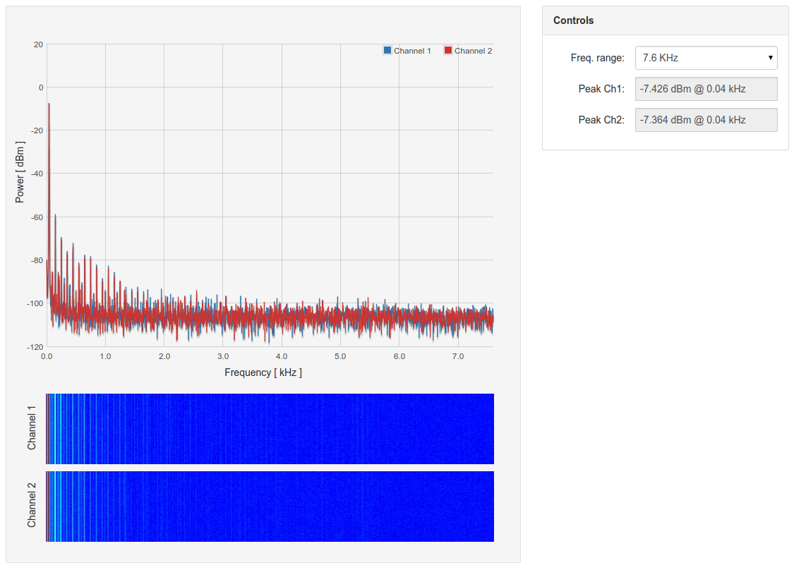
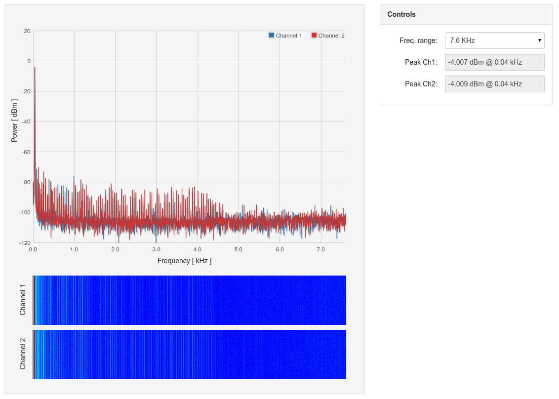
And, there’s more win. The USART MSPI has double buffering for the transmit function. This means that we can actually achieve a higher throughput using the USART MSPI than we can using the standard SPI bus! These logic traces demonstrate that the my best implementation of the SPI interface requires 4.58us to transmit a “frame” of information, consisting of two 12 bit samples. Using the USART MSPI interface we can achieve 4.25us per frame.

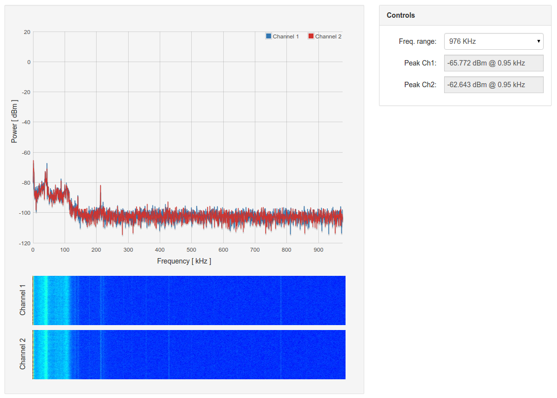
DAC control using SPI bus.

DAC control using USART MSPI bus.
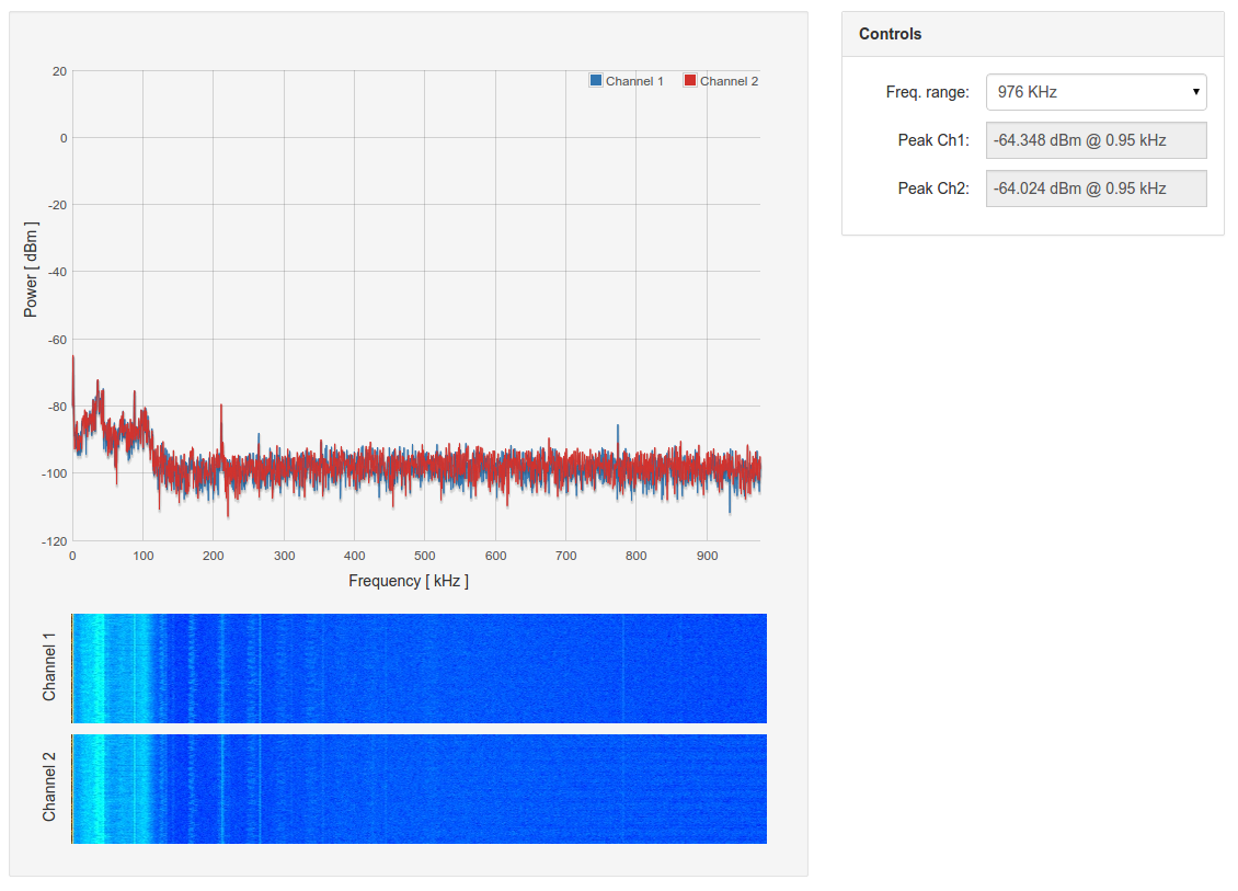
Either way, achieving 44.1kHz stereo output is not an issue. This trace shows the time spent in the DAC-out interrupt for a simple function, with the samples being played out at 44.1kHz.
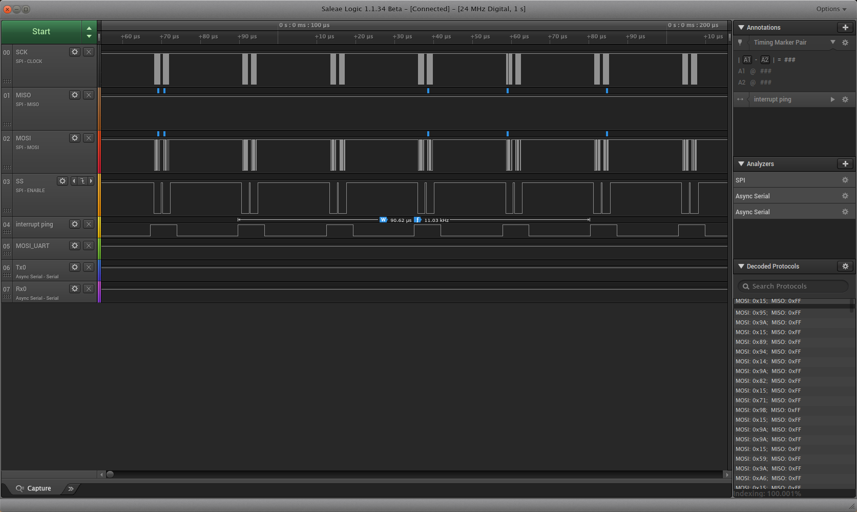
44.1kHz samples using USART MSPI output.
Guessing that this would be a great outcome, I ordered new PCBs from Seeed which implement the new pin assignments for the MCP4822. They will be here shortly.
My Revision Plans
Revert the uSD card 3V SPI bus drivers back to the quad and single buffers. The TXB/TXS story remains unresolved, and I can’t be bothered to work out why, when a simple answer is at hand. – DONE
Connect the uSD _CARD_DETECT to PC2 which has no other function except JTAG. – DONE
Remove the FTDI 6 pin for USART0. Or, better to move it to connect to USART1, so that USART1 can be addressed by an external FTDI device. Move it to the end of the board, so it doesn’t block Shield usage. Note the RTS/CTS Reset is not connected because this is replaced by a DAC A/B channel. – DONE
Remove the Analogue outputs from centre of board. Move them to the end of the board and integrate them into the FTDI USART1 socket on the RTS and CTS pin positions (obviously not on Tx or Rx pins, or on Vcc or GND either). – DONE
Connect the MCP4822 _LDAC pin to enable sychronisation of the A and B channels. Connect to PC3 which has no other function except JTAG. Remember the _LDAC is pulled to GND by default. – DONE
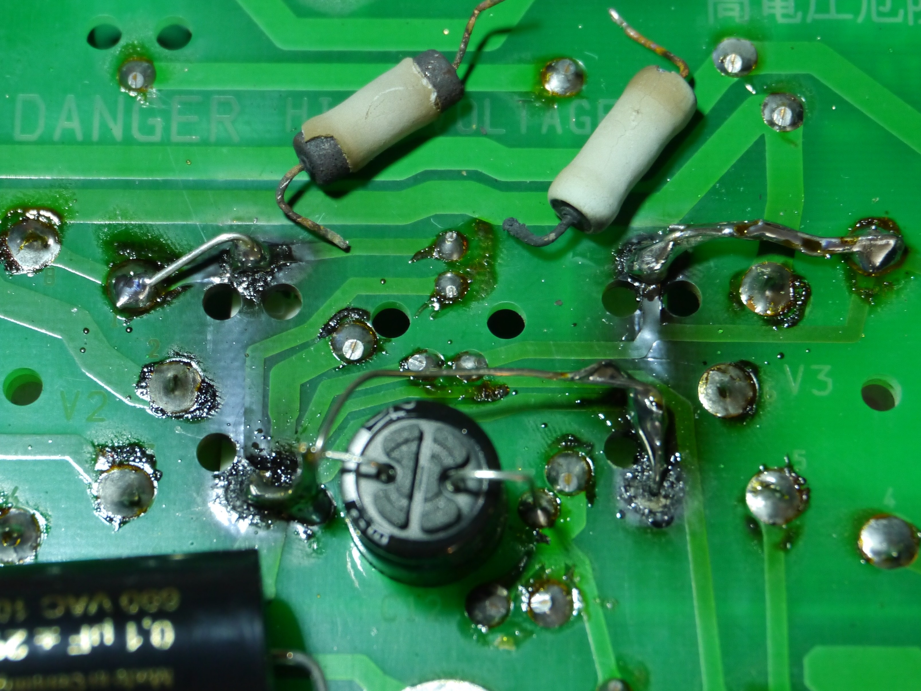
Have another look at the output filtering on the DAC, perhaps it could be a little stronger than the prototype with the corner at 23kHz. Single pole R1=68Ω C1=100nF. – DONE
This 2nd order filter is still linear, but filters significantly more (6dB rather than 3dB per decade) than the single pole version on the prototype.

2nd Order RC Low Pass Filter
Using standard Resistor and Capacitor values R1=47Ω C1=100nF R2=47Ω C2=100nF in a 2nd order CR Low-pass Filter Design Tool.
Extend the prototyping area by three columns. – DONE
Add a pin-out to allow the DS3231 RasPi module (battery or super capacitor) from Seeed Studio to be easily attached. Unfortunately, the devices I have don’t implement an _INT/SQW output, so alarms and wake on alarm won’t be possible. – DONE
Push the JTAG pads to the back of the board, without forgetting to flip the pin layout around. – DONE
Add SRAM or FRAM SPI storage. FRAM is non volatile storage, that has no delay. With a reasonable amount of storage we can use it to provide short audio samples, and get them back relatively easily, without file system and uSD card overheads. But FRAM is pretty expensive, and SRAM chips with same pin-out are available for much cheaper, that might fulfil the job of buffering or capturing samples.
MB85RS64V FRAM is the only reasonable device available for 5V supply. And it is a reasonable price of $1.80 per unit. But it is much too small to use as an analogue sample store. Need to use the 128kB MB85RS1MT FRAM version, but this required being driven from Vcc 3V3. At 8kHz sampling, 128kB gives us 16 seconds of sound, which is quite a lot. It costs around $6 which seems to be the sweet spot in pricing now. Will have to add another 3V3 to 5V MISO buffer. Use PC4 as the MB85RS1MT SPI _SS line.
Alternatively, just make the pinout for SPI 5V and implement SRAM using the Microchip 23LC1024 device, which is $2.50 each. We can choose FRAM or SRAM at assembly. Or even both, as there is a spare _SS available. So let’s do two devices at Vcc 5V supply.
Put 10kOhm pull-up resistors on all of these _SS lines, _CARD_DETECT and _HOLD. – DONE
Add 10kOhm pull-down resistors on _LDAC allowing active _LDAC control but not requiring it. – DONE
Convert the 3.3V regulator to AP1117 type in SOT89-3 package. No space for SOT223. Upgrades the 3.3V supply from 150mA to 1000mA. Heat spread on Layer 2 GND and on Layer 15. – DONE
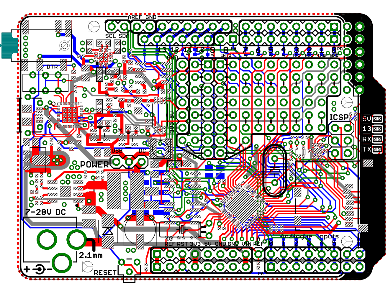
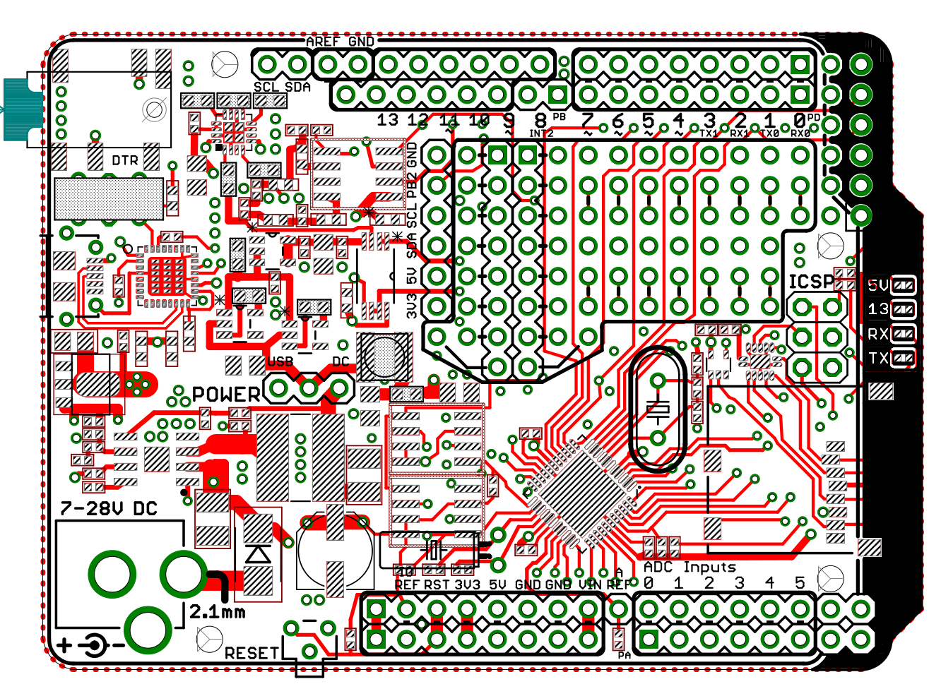
Initial Board Layout
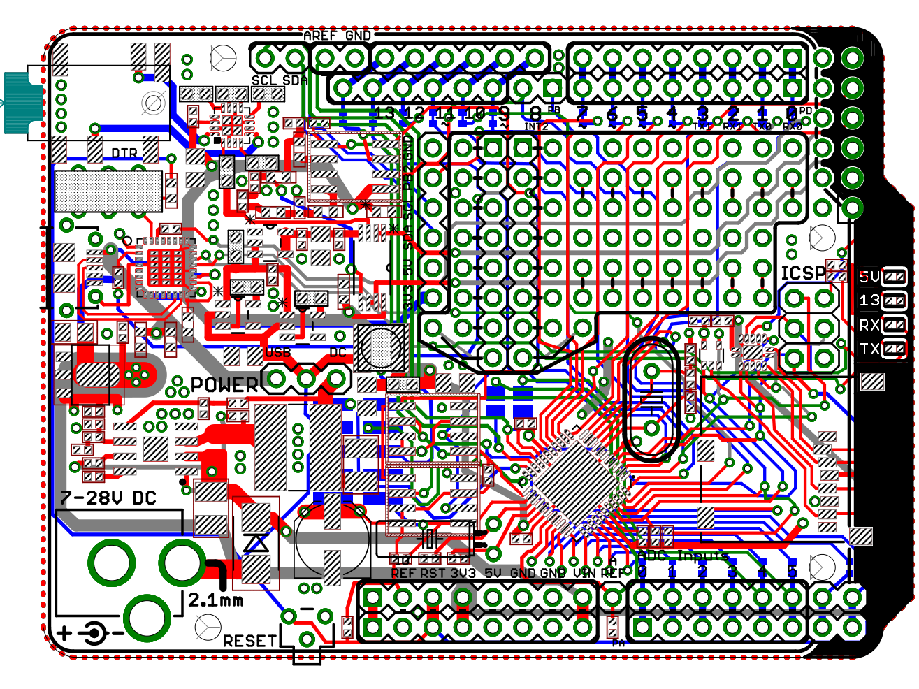
I’ve finished the schematic and the board layout, and now I just have the detailed work of checking all the things, again, and again. I’ve come back to this after letting it stew for a few days with the thought of changing just one component. But, as usual have made a host of minor adjustments that should make it better. These include further clearance of the ground plane under the analogue components, and untangling and straightening signals and vias where possible.
The Goldilocks Analogue Schematic in PDF format.
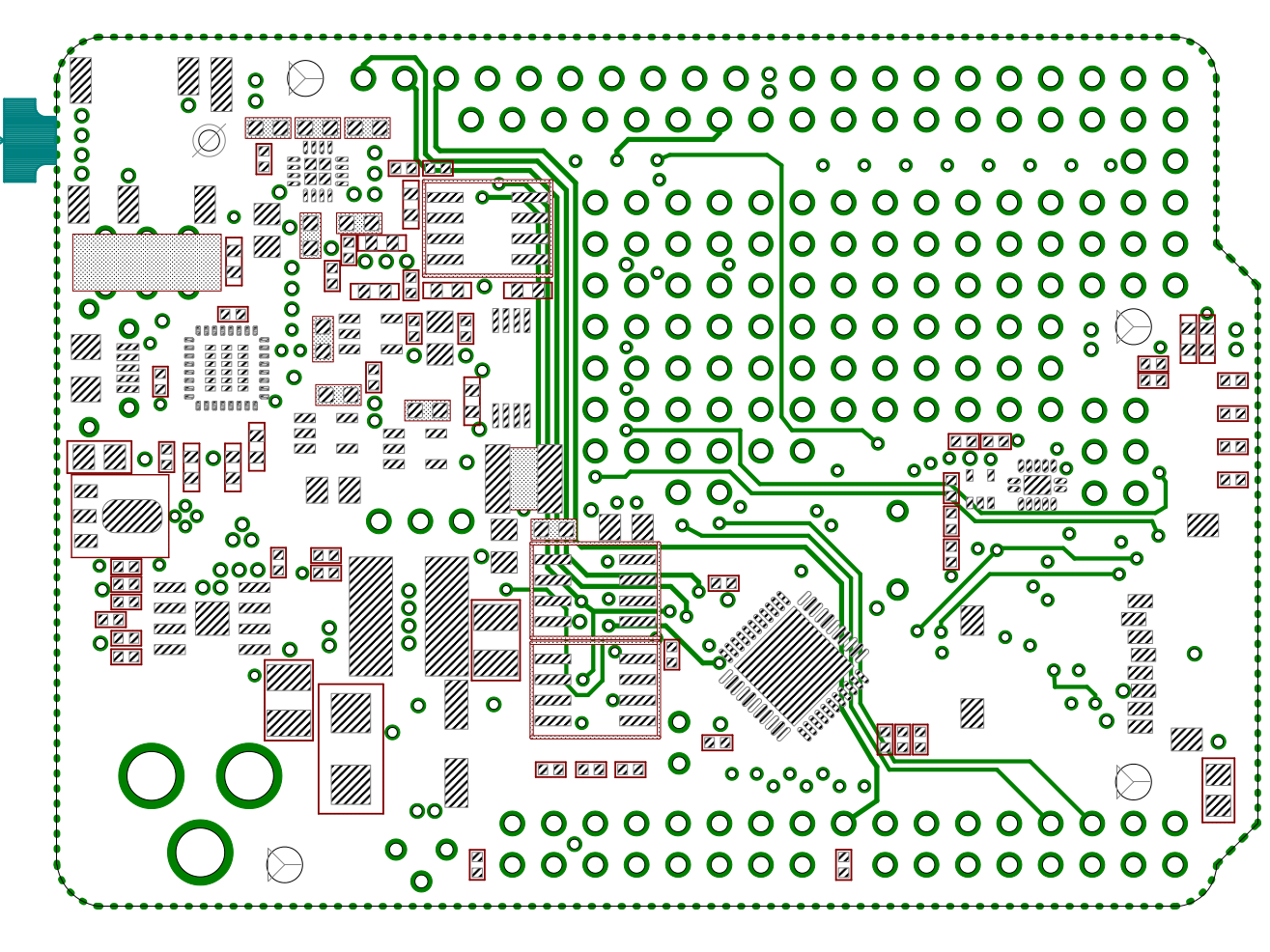
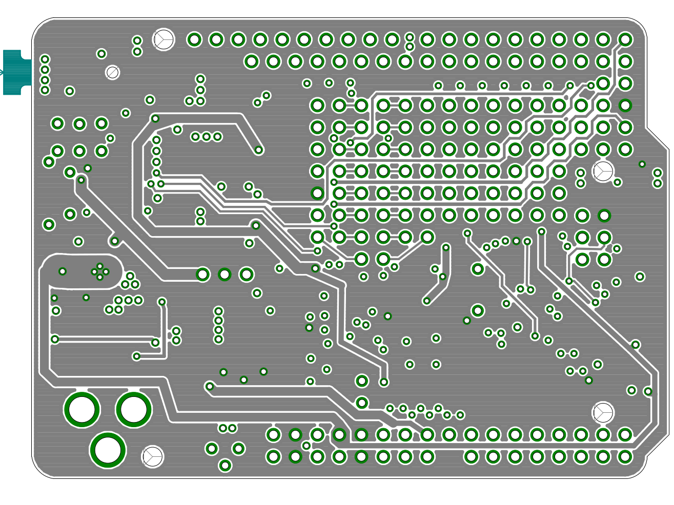
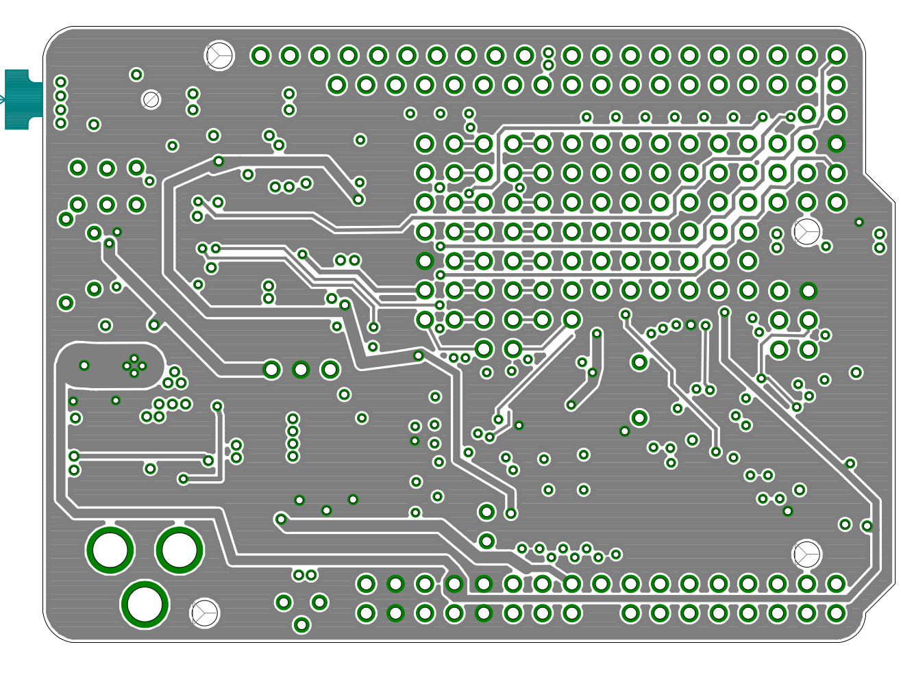
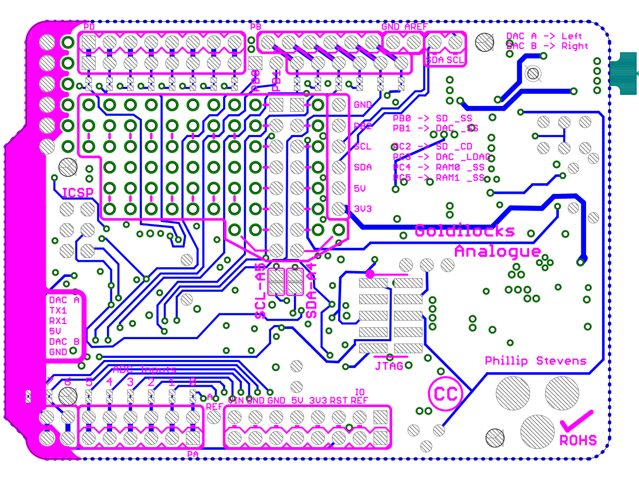
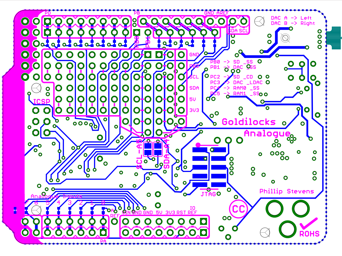
Front of board (All Layers)
The board is now pretty tightly packed. But, there is still a large number of options for prototyping on the board, or to exit the board with 8-pin headers. Each of Port A, Port B and Port D can be taken off board with one header each. Alternatively, a 2×8 connector can be attached, with the pins assigned and connected as desired.
The DAC A (L) and DAC B (R) channels are integrated into the far right edge of the board, along with TX1 and RX1 pins in the form of a FTDI 6 pin interface (including 5V and GND).
The first 5 pins of Raspberry Pi IO are replicated, to allow DS3231 RTC modules (designed for RaspPi) to be connected. For permanent mounting, the module can be flipped on its back to show the battery, and be mounted over the DAC which keeps the prototyping area clear.
I have been able to fit 2x SPI SRAM (or FRAM or NVRAM or EEPROM) on the board, using the spare JTAG IO pins. It is very tight, but having the option to fit up to an extra 2Mbit of SRAM will be quite useful for buffering and storing large amounts of data (audio, or samples).
15th April
The finished boards are now in my hands, and testing of the new SPI EEPROM and SRAM capabilities, together with MSPIM interface for the DAC begins.
Goldilocks Analogue – Prototype 3
Of course, new features are coming to mind. I’ll be putting them into the fourth prototype, which should come soon.
9th March
The blue PCB are back. Everything looks in order. The board is almost identical to the previous one. Just the change to the SPI attachment of the MCP4822 DAC to use the second ATmega1284p USART in MSPI mode.
The boards are now being built, and should be finished by the end of March. Looking forward to testing. I’ve requested that the boards be build with 2Mbit EEPROM and 1Mbit EEPROM combined with 1Mbit SRAM options. I don’t think having FRAM will be useful as the storage capability will be too small and too expensive. The EEPROM option will allow up to 16 seconds of high quality audio samples to be stored (without using an SD card). The SRAM option will allow samples of audio to be stored, and then used to play back, but given quality will only be 8 or 10 bits because of the inbuilt ADC capability, up to about 16 seconds can again be recorded.
Goldilocks Analogue – 2x SPI Memory Devices
16th February
Major revision. Moved the DAC control to use the USART1 MSPI function. It will be connected to Arduino Pin 4 XCK1 and Pin 3 TX1. This will ensure that we can stream data from the uSD card or the FRAM/SRAM/EEPROM on the main SPI bus to the DAC on the USARTt1 MSPI bus with no contention issues.
PCB with the revised connections is on its way.
21st January
The boards are back. Everything looks in order. The concept of using the keep-out layer to write in silkscreen works as hoped, so the labels on the edge are legible.
Time to get to ordering the new components, and building.
Goldilocks Analogue – Prototype 3
31st December
Cleaned up the board to allow more labels to be applied, trying to make it self-documenting. Packed the analogue section a bit tighter, and improved the power routing.
21st December
Cleaned up many traces and cleared the Layer 2 GND plane even more. Discovered the DS3231 modules don’t implement the _INT/SQW function, but leaving the connection to PB2 (INT2) on the pin-out for the future.
16th December

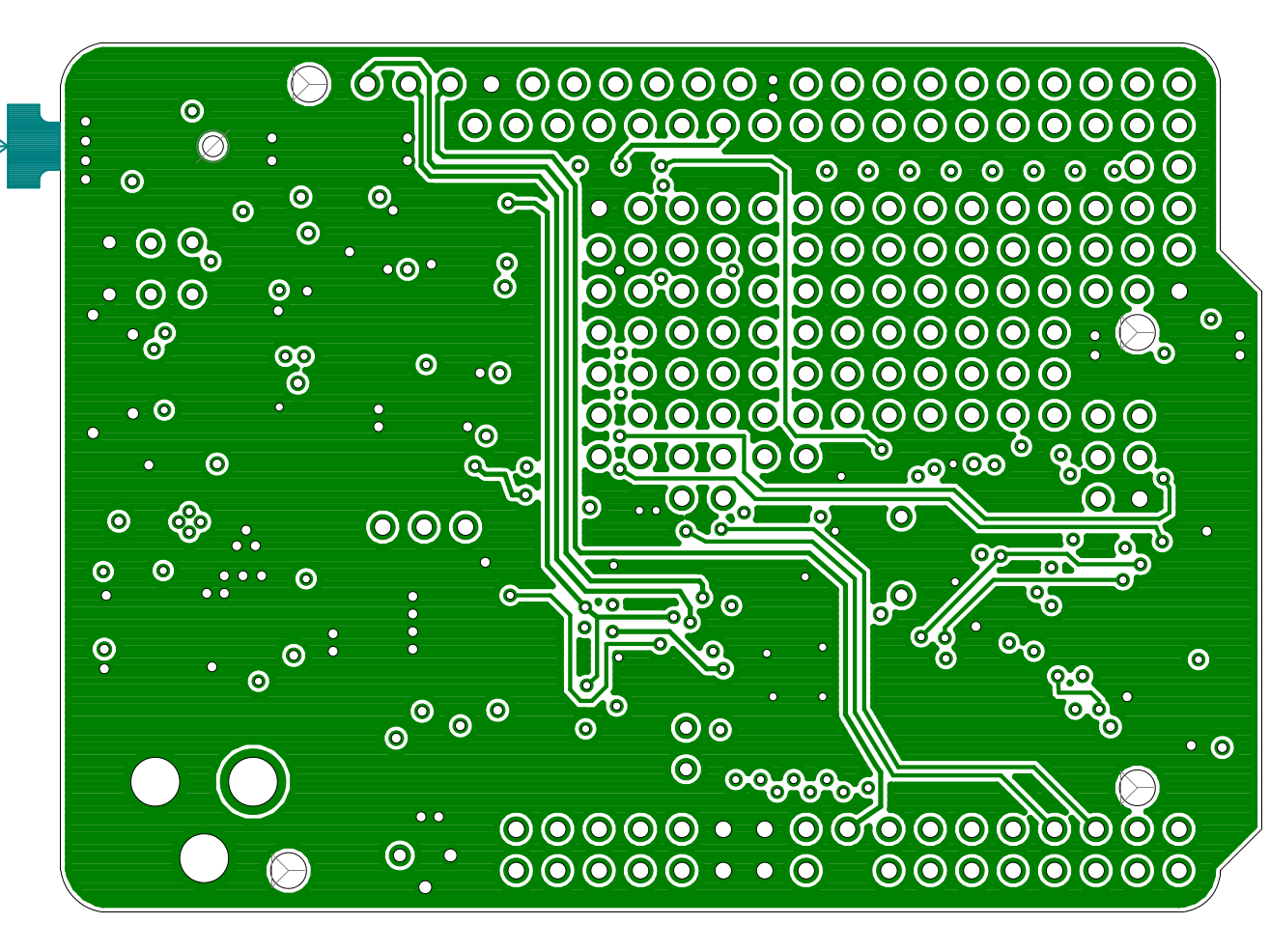
Top Layer
Labels for the DAC A and DAC B and FTDI interface have been put into the keep-out layer in the silk screen on the edge. They will appear when the silk is printed.
Added Test Points for the 3.3V SPI signals, which are the only signals that can’t be tested off a pin-out somewhere.
31st December
Added labels for the I2C (Raspberry Pi IO1 through IO5) pin out, by moving the analogue section left.

21st December

16th December

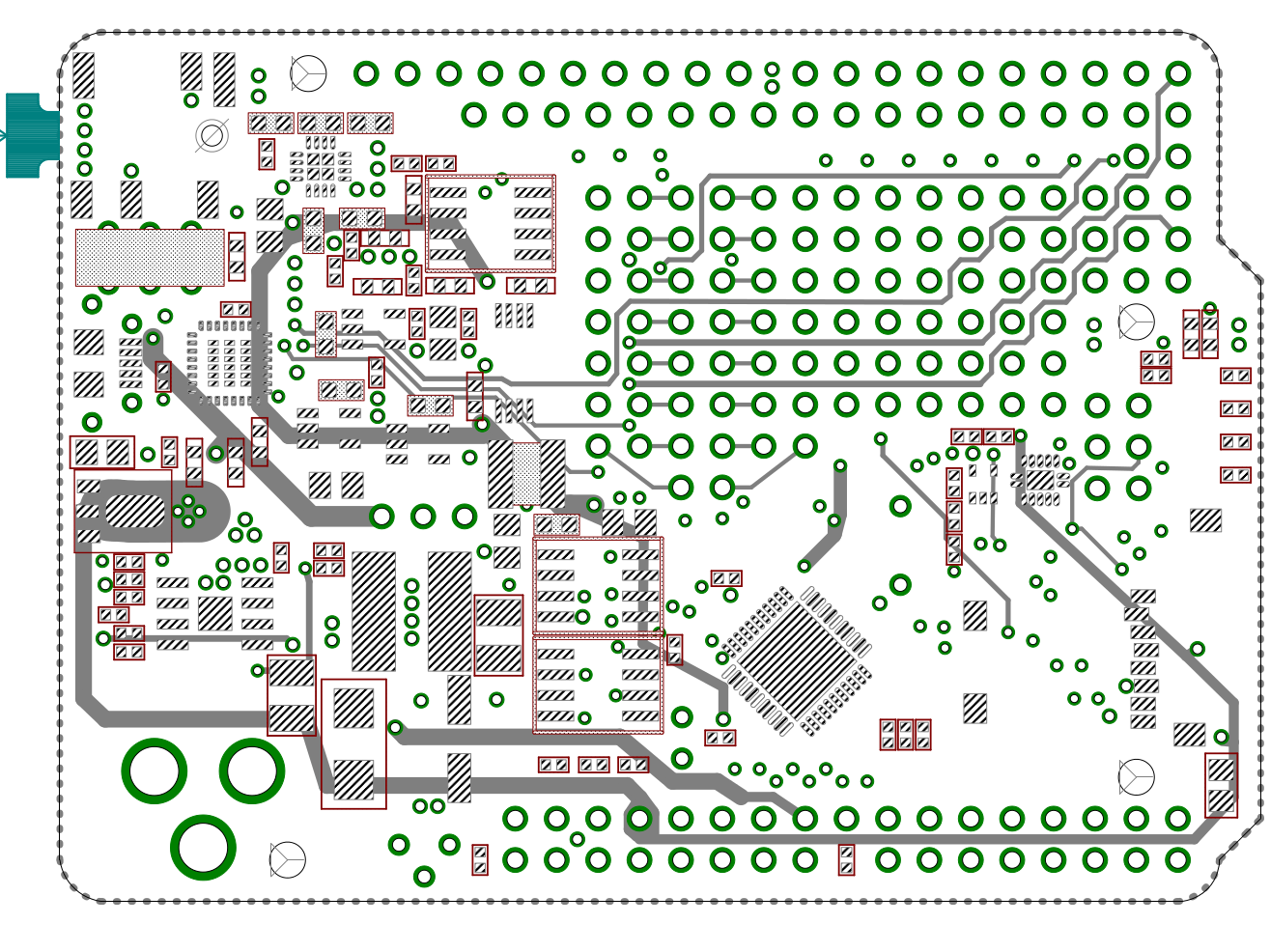
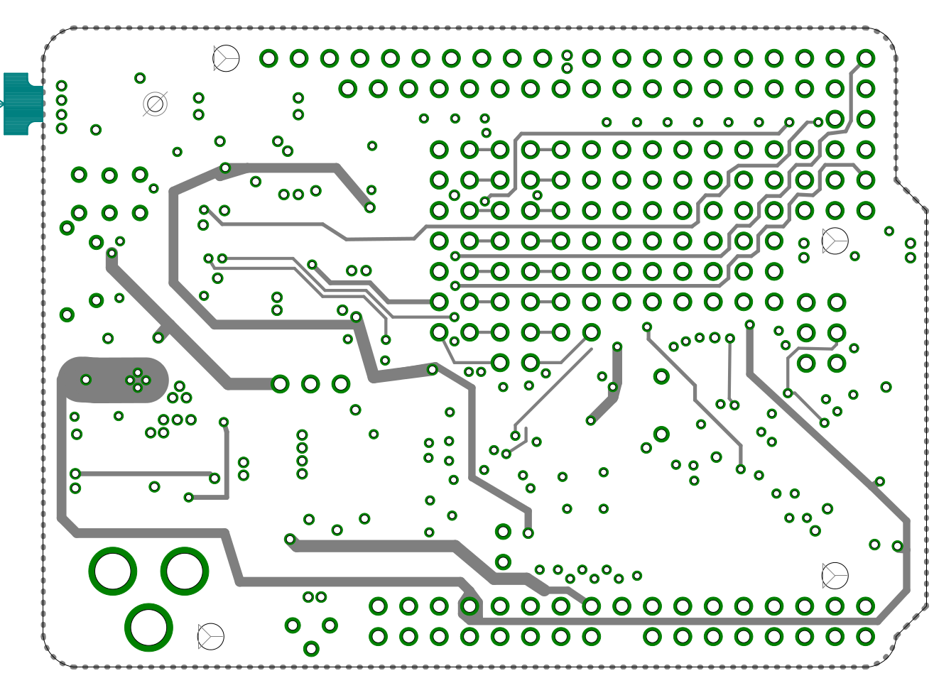
Layer 2 – GND
The GND plane remains whole under the DAC and Amplifiers.
31st December
Moving the analogue section to the left and compressing it moves components more over the solid ground plane.

21st December
Improved the ground plane by moving traces out from under components, and re-routing AVCC line.

16th December

Layer 15 – 5V (and 3.3V)
The 5V layer, with the 3.3V and AVCC 5V supplies too.
31st December
Resolved the S-bend power to the I2C 5V pin out, and removed some dead traces.
21st December
Kept the 5V AVCC line on this layer which makes it longer, but avoids using vias. Tidied up some other power routing.
16th December
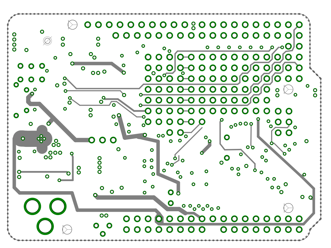
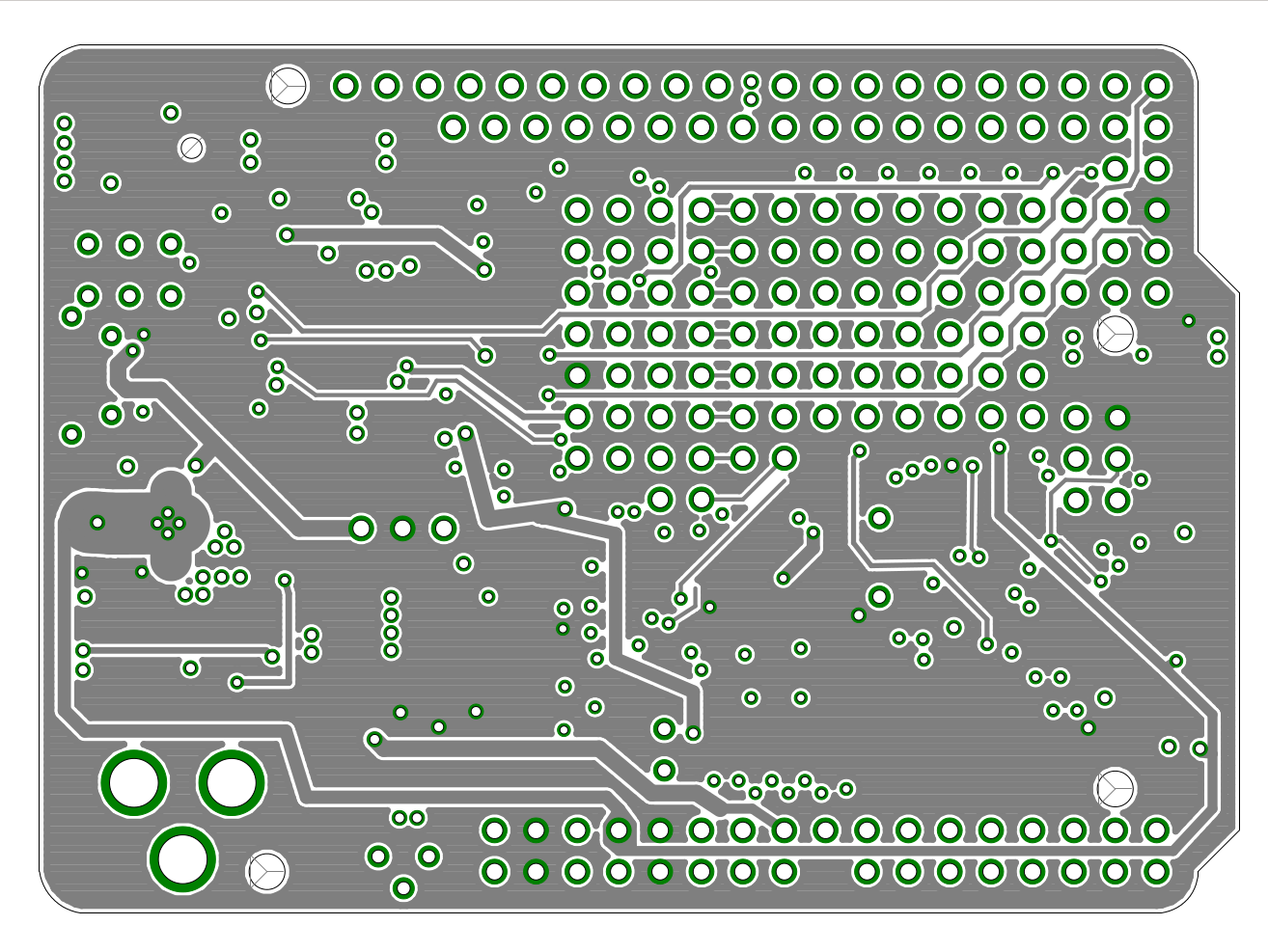
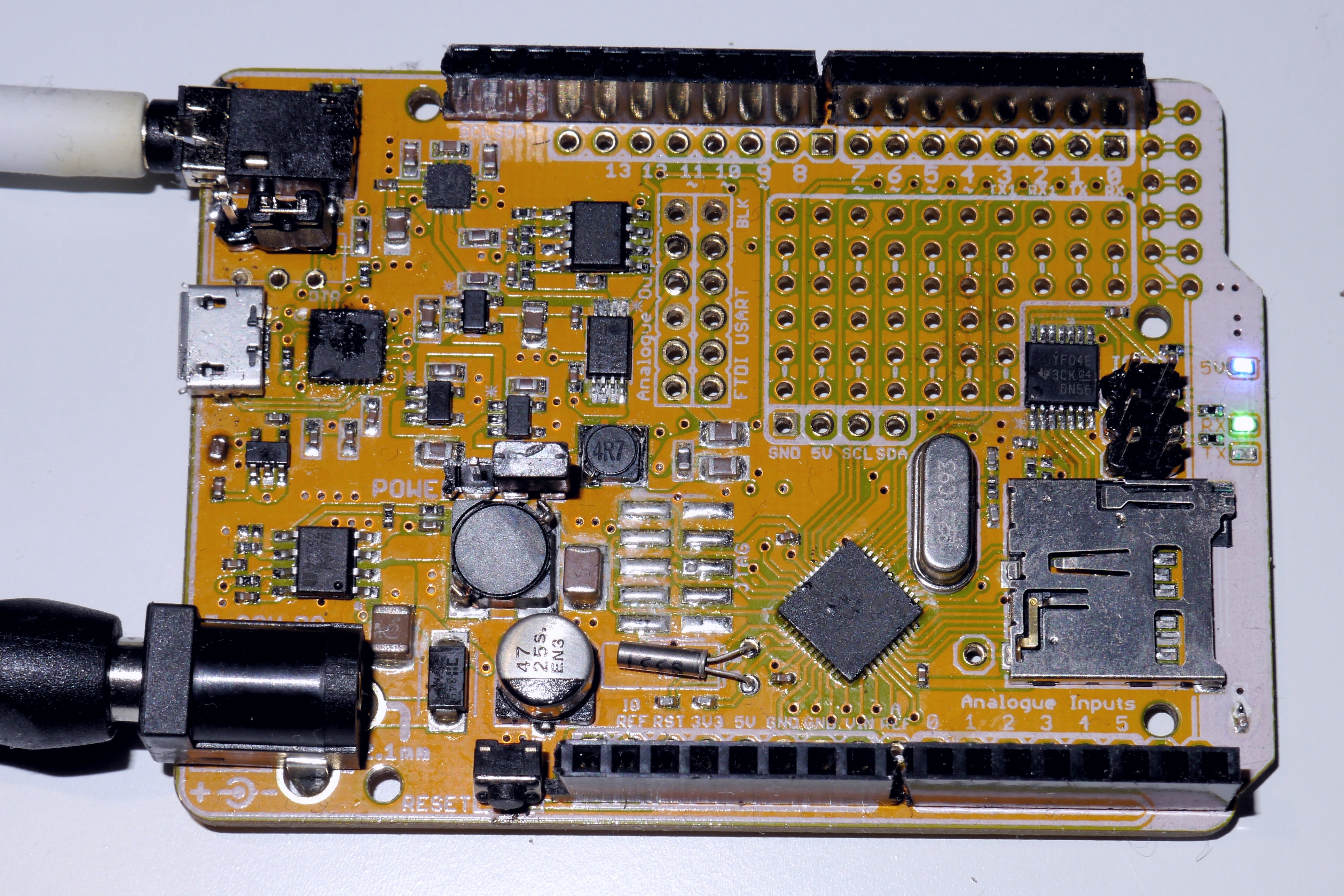
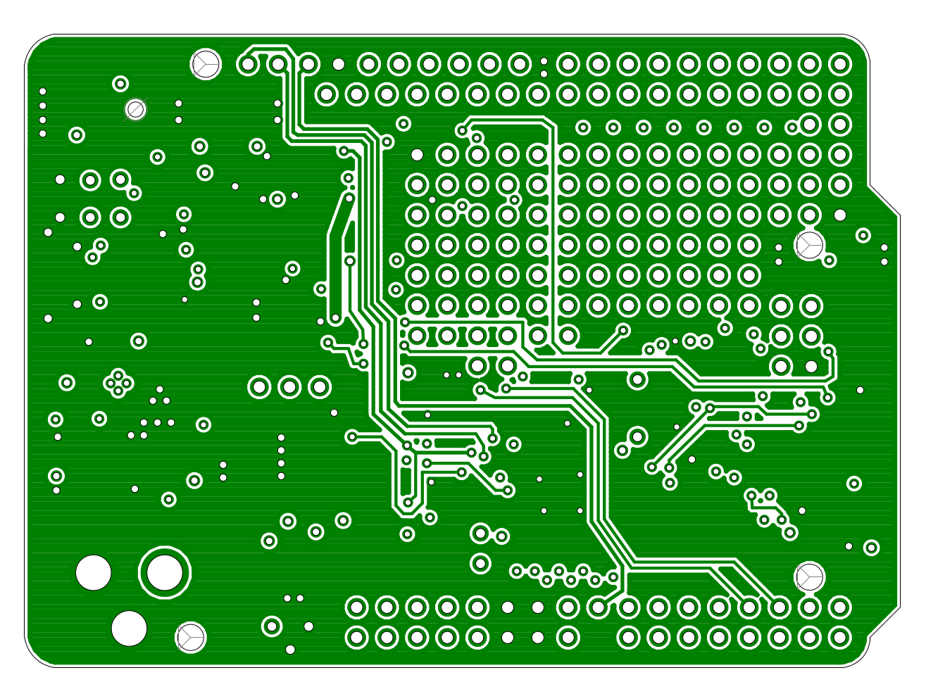
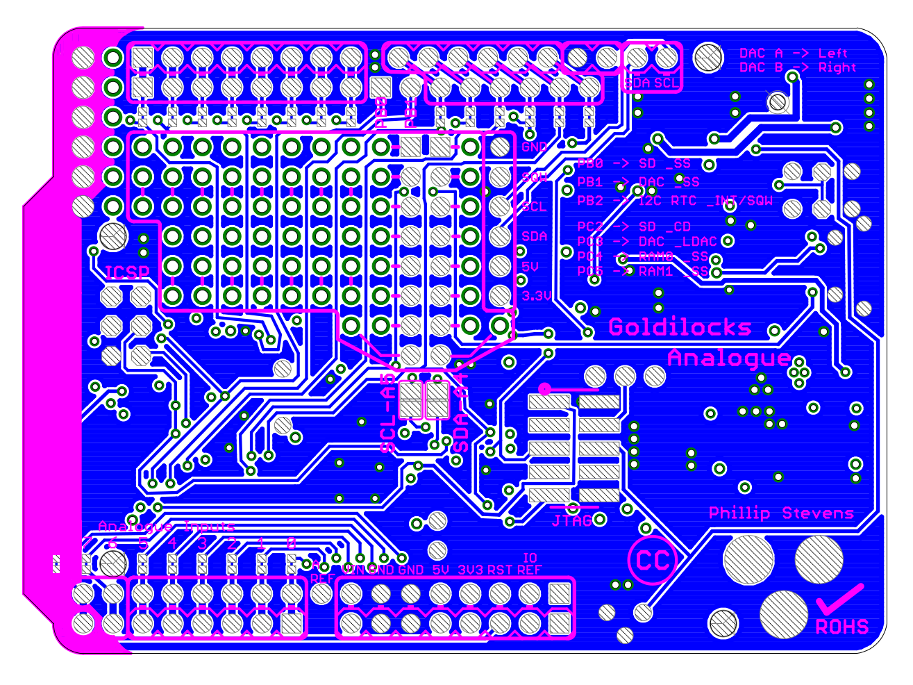
Bottom Layer
All the pin-outs are defined on the bottom. Unfortunately, there is no space on the top layer.
The JTAG is now pushed to the back of the board. This will make using the JTAG more difficult, but at least it will not interfere with shields, should the solution require testing when in a system.
9th March 2015
The back side is clean, and all of the labels are unchanged.
Goldilocks Analogue – Prototype 3
21st January 2015
The back side is clean, and all of the labelling will ensure that the board is self documenting. I was unsure whether putting text in the keep-out layer would work, but it seems to work very well. That’s a win.

Goldilocks Analogue – Prototype 3
31st December
Added labels for the “FTDI like” pin out, combined with the DAC outputs, to improve self documentation.

21st December
Added more accurate descriptions, and tidied some routing.
16th December

Pin Mapping
This the map of the ATmega1284p pins to the Arduino physical platform, and their usage on the Goldilocks Analogue
| Arduino UNO R3 |
328p Feature | 328p Pin | 1284p Pin | 1284p Feature | Comment |
| Analog 0 | PC0 | PA0 | |||
| Analog 1 | PC1 | PA1 | |||
| Analog 2 | PC2 | PA2 | |||
| Analog 3 | PC3 | PA3 | |||
| Analog 4 | SDA | PC4 | PA4 | PC1 I2C -> Bridge Pads | |
| Analog 5 | SCL | PC5 | PA5 | PC0 I2C -> Bridge Pads | |
| Reset | Reset | PC6 | RESET | Separate Pin | |
| Digital 0 | RX | PD0 | PDO | RX0 | |
| Digital 1 | TX | PD1 | PD1 | TX0 | |
| Digital 2 | INT0 | PD2 | PD2 | INT0 / RX1 | USART1 |
| Digital 3 | INT1 / PWM2 | PD3 | PD3 | INT1 / TX1 | USART1 -> MCP4822 MOSI |
| Digital 4 | PD4 | PD4 | PWM1 / XCK1 | 16bit PWM -> MCP4822 SCK |
|
| Digital 5 | PWM0 | PD5 | PD5 | PWM1 | 16bit PWM |
| Digital 6 | PWM0 | PD6 | PD6 | PWM2 | |
| Digital 7 | PD7 | PD7 | PWM2 | ||
| Digital 8 | PB0 | PB2 | INT2 | <- _INT/SQW | |
| Digital 9 | PWM1 | PB1 | PB3 | PWM0 | |
| Digital 10 | _SS / PWM1 | PB2 | PB4 | _SS / PWM0 | SPI |
| Digital 11 | MOSI / PWM2 | PB3 | PB5 | MOSI | SPI |
| Digital 12 | MISO | PB4 | PB6 | MISO | SPI |
| Digital 13 | SCK | PB5 | PB7 | SCK | SPI |
| (Digital 14) | PB0 | T0 | -> SDCard SPI _SS 3V3 | ||
| (Digital 15) | PB1 | T1 | -> MCP4822 SPI _SS | ||
| SCL | PC0 | SCL | I2C – Separate | ||
| SDA | PC1 | SDA | I2C – Separate | ||
| PC2 | TCK JTAG | <- _CARD_DETECT for uSD Card |
|||
| PC3 | TMS JTAG | -> MCP4822 _LDAC | |||
| PC4 | TDO JTAG | -> RAM SPI _SS_RAM0 | |||
| PC5 | TDI JTAG | -> RAM SPI _SS_RAM1 | |||
| PC6 | TOSC1 | <- 32768Hz Crystal | |||
| PC7 | TOSC2 | -> 32768Hz Crystal | |||
| XTAL1 | PB6 | ||||
| XTAL2 | PB7 | ||||
| (Analog 6) | PA6 | -> Pad / Hole | |||
| (Analog 7) | PA7 | -> Pad / Hole |
Discussion on RTC
At the end of the day, the DS3232 / DS3231 device is around $8 best case to me. But modules are available complete with super capacitors from Seeed for around $6. There’s no win here. Stick to the crystal and existing solution, but make it easier to use the Seeed RasPi solution.
Digikey has the DS3231 at $8 per piece. This is pretty expensive, for what it delivers. And there are solutions available with super capacitor backing for under $6 from Seeed.
Design in the DS3232 on the TOSC1 input for the TCXO 32kHz clock and PC5 input for the INT/SQW line. Supply from 3V3 Vcc. Read that the I2C lines can run to 5V5 without issue. INT/SQW outputs are open drain and the INT/SQW can be disabled (high impedance). Let the ATmega1284p switch on its pull-ups for INT/SQW to function. Make sure 20kOhm pull ups on the SCL/SDA lines too.
The DS3232 has 236 Bytes of SRAM, and a push-pull output on TCXO 32kHz line so this is better as an asynchronous clock input.There is an accurate (0.25°C) thermometer function included. It comes in an 20SOIC package which is quite large. Having some SRAM will be very useful for storing configurations that change often (where EEPROM would wear out).
The DS3232M has 236 Bytes of SRAM, and a push-pull output on 32kHz line so this is better as an asynchronous clock input. Having some SRAM will be very useful for storing configurations that change often (where EEPROM would wear out). But, it doesn’t have 5.5V capability on its I2C lines. – Deselect
The DS3231 version comes in an 16SOIC package, which might be better, but it doesn’t have any SRAM, and the TXCO is open drain. – If we need smaller then this is where we go.
The DS3231M MEMS version comes in an 8SOIC package, which might be better, but it is only +-5ppm (rather than +-2ppm). – Don’t need the small package, so go for XTAL version DS3231 in the SOIC16 package.
Digikey has the DS3232 at $8.60 per piece. This is pretty expensive, for what it delivers.
Delete the 32kHz crystal, and capacitors.
Add on a 3V Lithium battery holder. Or a Super Capacitor and a charging diode
Leave the TOSC2 pin floating, as it is not useable when the Timer 2 Asynchronous Clock Input is enabled on TOSC1.
Remove pull-up resistors from RST, as the DS3231 has pull-ups as does the ATmega1284p. The DS3231 has a debounce and 250ms delay function to manage the MCU start up.
Design Input from Angus
IC6 is missing silkscreen marking for pin 1. – DONE
Designator layer needs a cleanup. I had to spend a lot of time in
EAGLE checking which components were which, and what orientations
they had. On such a full board with close-spaced components this is
very important – ideally place each designator between the pads it
refers to, with a consistent orientation relative to the pads. – DONE
Some 0603/0402 components seemed to have wrong pad sizes compared to
BOM output, ie R17 & C13. I placed according to what parts were
supplied. I know this has been revised further but it might be worth
checking BOM output for any remaining anomalies. – CHECKED
If possible move components away from IC bodies, for example C36 is
very close. Even for a pick & place machine I suspect this would be
hard. – DONE
Labels on silkscreens would be very helpful. For instance the power
selection & DTR jumpers, other pin breakouts. For Freetronics boards
we aim to have all of these connections self-documenting, ie each
option labelled somehow. This can be difficult but part of the
appeal of a development board is being able to easily make
customisations without requiring an external reference. – DONE
It’d be great if you could find a way to better convey the offset
pin numbering for pins 8-13. – NO BETTER ANSWER
The MCU 1284p solder stencil paste layer has too large of an
aperture for the thermal pad. If you look at the paste layer of IC1
and compare to IC2 then you’ll see what I mean. The aperture needs
to be cut down in this way or the central pad gets too much paste
and “floats” up, leading to the outer connections not forming
correctly. – OK Can’t change Library
Suggest adding test points for likely problem connections. ie
analogue section power rails, 3.3V SPI connections, raw DAC
outputs. These can just be bare SMD pads on top or bottom of
board. Label with a designator (at least) or a descriptive label if
possible. For an example of what I mean, the OpenVizsla boards have
a really nice set of 4 power test points near the bottom of the
board. – DONE Power is easy off pins. Added 3.3V SPI test points. Other pins all have pin-outs.
Design Input from Freetronics Forum
Keep the JTAG header, but also distribute the pins to the 2nd Non-Arduino shield pins. – Going to push the JTAG to the back of the board. It will be inconvenient to use, but won’t block the use of Shields when it is actually being used so this is better. This also frees more space for a RTC and battery option. – DONE
Add a RTC option. – Using the 32kHz crystal on Timer 2 the RTC is working fine. Battery and power options can be off board, and as comprehensive and accurate as needed. – DONE
Other RTC options include using the DS3231, which would be more accurate than a 32kHz crystal, and includes an integrated RST debounce timer. Can use the 32kHz output to feed the ATmega1284p Timer 2 and therefore have both devices locked to the same clock. Chronodot as an example for using this RTC. – DONE