
The Pozible project for Goldilocks boards is funded and closed.
Pozible Goldilocks
As featured in Make.
Freetronics Goldilocks is now sold out.
Freetronics Goldilocks
But, Freetronics are considering making a new version.
Please add your wish list here.
Also, I’m working on a new version, Goldilocks Analogue with an integrated dual channel DAC. Now a second prototype of the Goldilocks Analogue has been designed and tested. It has taken a year, because I’ve been using the existing Goldilocks boards for a number of projects. Now I’m designing (hopefully) the final iteration of the Goldilocks Analogue before it goes into production.
I have a Kickstarter project to get the Goldilocks Analogue into production. The project was successfully funded.

Updated Firmware for Goldilocks (Pozible & Freetronics)
- LUFA 140928 for ATmega32u2 DFU and for U2duino (USB to USART).
- Increased bootloader timeout for ATmega1284p.
- Updated IDE file structure to provide support for Arduino IDE 1.6.x.
- Renumbered I/O pins for greater commonality with Arduino core.
- Also added a Goldilocks Analogue Bootloader, running at 24.576MHz
Look for Goldilocks in the Unofficial Boards Support List, and follow the instructions in the Goldilocks Analogue User Manual.
Background
This proposal is to implement an Arduino clone using the ATmega1284p MCU, as replacement for the normal ATmega328p MCU, bringing significant improvements and longevity into the existing Arduino platform.
The current Arduino Uno and Leonardo devices cater for many applications, but they are becoming limited for some modern applications, such as Ethernet networking, SD Card storage, and USB based systems. The limitation in SRAM in the 328p and 32u4 is the most apparent issue, and this is the most difficult to supplement with external components. The Uno R3 platform is too small for demanding applications, and therefore not the right solution.
Arduino Mega devices are available which provide more RAM (but still less than Goldilocks) and many more interface pins, but unfortunately many of the standard Arduino Shields will not work with the Mega, unless you are prepared to hack them. The Mega platform is too big for the standard Shields, and therefore not the right solution.
Arduino and others are moving towards 32 bit MCU devices, including ARM Cortex based platforms such as the Arduino Due, which brings significantly more resource into play, but these platforms will require a major re-education of users, and may actually fragment the Arduino user group. Also, these ARM processor based devices must be operated at 3.3V and can only supply 4mA per I/O, which makes them incompatible with many of the existing Arduino Shields.
I believe the Goldilocks solution is to use the Arduino Uno / Leonardo R3 physical format, for 100% Arduino Shield compatibility at 5V and with the standard pin layout. But using the ATmega1284p processor to provide significant improvements in RAM, FLASH, EEPROM, interfaces, and other factors.
I’ve been working with Arduino devices now for some years, and have found that my interest remains in fully understanding the way the “bare metal” processor is working. The Arduino platform gives me that opportunity.
https://sourceforge.net/projects/avrfreertos/
Whilst many argue that the days of 8 bit processors are numbered, and that devices such as the Raspberry Pi are the future, I would say that there remains a need for very simple, but very capable platforms, such as the “Goldilocks” platform proposed here. Raspberry Pi and others are essentially Linux machines, and are addressing different needs to this platform.
The 1284p MCU has already been used by the RepRap project as a platform in their minimalist Arduino platform, as a result of them experiencing similar resource limitation issues. The RepRap 1284p platform maintains Arduino code compatibility (boot-loader, board descriptions, avrdude) but abandons physical compatibility, as theirs is a special purpose application and has no need to support Arduino Shields.
http://www.kirbyand.co.uk/serendipity/index.php?/pages/Min644pWarez.html
http://www.kirbyand.co.uk/serendipity/index.php?/pages/min644p.html
Similarly Pololu use the 1284p in their Orangutan SVP platform, but again theirs is a special application, which incorporates many robotics interfaces, and deviates from both the Arduino physical and software platform. Pololu also implement an on-board ISP, which removes the need for the Arduino serial bootloader freeing more space for program code.
http://www.pololu.com/catalog/product/1327
Recently, others are starting to use the 1284p as the “Goldilocks” solution between 328p and 2560. This helps with establishing the precedent for the “Goldilocks” with the Arduino IDE and its hardware descriptions.
http://maniacbug.wordpress.com/2011/11/27/arduino-on-atmega1284p-4/
http://arduino.cc/forum/index.php/topic,64612.0.html
http://blog.stevemarple.co.uk/2011/11/calunium-pcb-version.html
http://www.bajdi.com/bajduino/bajduino-1284/
http://forum.freetronics.com/viewtopic.php?f=6&t=330
This is the final Goldilocks v1.1 board, that was prepared for Pozible Supporters.
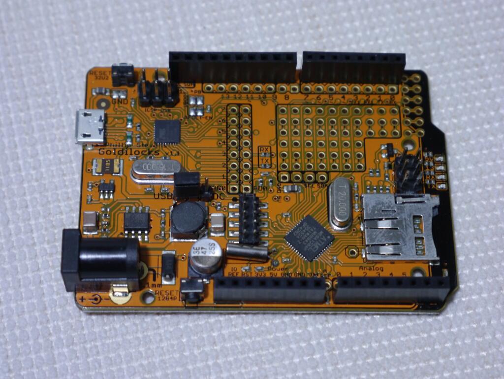
Here are some screenshots of the prototype board design.

Differences between 328p and 1284p
The ATmega1284p has a number of significant differences from the 328p that make it a great MCU for the Arduino platform. Some are listed below, in no particular order.
- 16kByte SRAM = 8x Uno SRAM
The 1284p has 8x more SRAM than the 328p, and also has double the SRAM of the 2560. There is no other AVR ATmega MCU with this much SRAM.
For Ethernet, video, and USB applications where large frame buffers need to be maintained or manipulated, the flexibility of having 16kByte of SRAM will change the kind of applications that can be implemented.
- 4x Uno Flash & 2x Uno EEPROM
The 1284p has 4x more Flash and 2x more EEPROM than the 328p and therefore can store larger programs and non-volatile data.
- 2x Programmable USART
The 1284p has 2 programmable USARTs. These appear on Digital pin 0,1 and 2,3. This allows users to maintain the serial monitor connection with the Arduino IDE, whilst addressing another application, such as a GPS device. For new users and experienced alike having two serial interfaces will be a big improvement.
- Independent Analogue Platform (separate I2C bus pins)
Using the SMD package for the 1284p allows the board layout to implement a fully independent analogue platform. This is because the I2C bus pins are on a separate port to the ADC pins, and the ADC pins have no “alternate function” except for the PCINT function. Also separate AVCC and GND pins allow the analogue PA Port to be powered and grounded separately from the digital section of the MCU.
- Timer 3 (Extra 16bit timer)
The 1284p has an extra 16bit timer, Timer 3, that is not present on any other ATmega MCU. Timer 3 does not have PWM outputs (unlike Timer 0, Timer 1, and Timer 2), and therefore is free to use as a powerful internal Tick counter, for example in a RTOS. freeRTOS has already been modified to utilise this Timer 3. Timer 3 (Extra 16bit timer)
- Timer 2 (Real Time Clock Oscillator)
The 1284p has a 32.768 kHz capable timer, that can be fitted with an accurate watch crystal to enable real time keeping. Use of the avr-libc time.h functionality (present only in upstream release currently) allows an efficient SystemTick to match with advance time and date functions.
- JTAG Interface
The 1284p implements a JTAG functionality which will allow advanced developers the option to debug their code.
- Better PWM access
The 1284p brings additional 8bit Timer 2 PWM outputs onto PD, which creates the option for 2 additional PWM options on this port. It also removes the sharing of the important 16bit PWM pins with the SPI interface, by moving them to PD4 & PD5, thus simplifying interface assignments.
- Extra I/O pins (e.g. for internal SS pins)
The 1284p has additional digital I/O pins on the PB port. These pins could be utilised for on-board Slave Select pins (for example), without stealing on-header digital pins and freeing the Arduino Pin 10 for Shield SPI SS use exclusively.
Design Improvements on “Uno”
- Add through-holes for all I/O
The existing Freetronics 2011 has space for prototyping, but doesn’t make any allowance for connecting pins to the prototyping space. Trying to solder jumpers between the I/O pins on the board backside is not very pretty, and also not robust for permanent prototyping. The Arduino Uno or Leonardo doesn’t have any prototyping space at all.
Suggest to include a row of through-holes inside the each of the pin headers to allow a header or jumper to be soldered to the I/O lead effectively.
Align the rows of through-holes to the 1/10” pitch, and to prototyping area pin pitch, to allow “Goldilocks” to have header pins soldered on the bottom, and be inserted into a standard breadboard.
- Replicate SPI and I2C to through-holes (with additional 1284p Alternate SS I/O).
The SPI and I2C interfaces are used for many daughter card options (from Sparkfun for example). Some examples include RTC, acceleration & magnetic sensors.
These mini-cards need access to the SPI or I2C interfaces which are shared with I/O pins. Bringing these SPI and I2C pins with Vcc and GND onto through-holes in the standard order (of Sparkfun cards, for example) at the left and right ends (respectively) of the prototyping area would simplify prototyping with these interfaces.
This is now implemented on the Arduino Uno Rev 3. as additional pins for I2C.
http://www.arduino.cc/en/Main/arduinoBoardUno
But, the additional through-holes remain valuable for the prototyping area.
- Add JTAG Interface
Adding a standard JTAG interface at the edge of the card would allow in circuit debugging to be implemented. Whilst there may not be sufficient space to implement a standard JTAG connector, there would be space to bring the JTAG pins onto through-holes for headers.
- Add a Micro SD Cage
There is space to add the long term storage capability brought by an integral Micro SD Card cage. Many projects require logging of sensor data, or capturing or playback of information, and the Micro SD card format is the easiest way to get data onto and off of any format of PC or Smartphone. The ATmega1284p also has plenty of SRAM to allow large buffers for reading and writing to the Micro SD card, so it makes sense to include it as a most needed option.
- Link ATmega32u2 and ATmega1284p SPI interfaces
The USB-serial interface on the Uno is implemented by a ATmega16u2 device, but its SPI bus is only connected to the SPI programming header, and the SS pin is not even brought out. The Goldilocks will allow the ATmega32u2 MOSI, MISO, CLK, pins to to be easily bridged (solder pads on rear of board), and bring the SS pins of both ATmega devices to a patch pad. This will allow the two devices to work in concert for demanding multi-processing applications, involving USB and other peripherals.
- Isolate analogue platform (optional SCL & SDA bridge)
For some applications digital noise and voltage droop (when using servo PWM), can have a significant impact on the accuracy of ADC conversions. Using the SMD 1284p it is possible to completely electrically isolate the digital Vcc and analogue AVcc and GND planes, as well as isolating the ADC converter within the MCU. A separate rectifier, or low pass filter could be used to provide AVcc.
The option to bridge the 1284p I2C pins on SDA and SCL with A4 and A5, where needed for compatibility with Arduino Shields, should be maintained through the use of solder bridges.
- Move Reset to edge
It is more common to need to use the Reset button with a shield in place, and if the Reset button is placed close to the edge (even vertically mounted, like the Seeed ADK main board), it can still be reached with a fingernail. Arduino Uno R3 implements this by moving Reset to the upper edge, near the USB connector.
- Clock at 20MHz (or 22.1184MHz)
There is little reason to continue to run the MCU at 16MHZ, and given the MCU is specified to 20MHZ, being able to do 5 things, where previously we could only do 4, seems like a worthwhile improvement. Also, the use of a through hole precision crystal (not a SMD resonator) allows the use of after-market timing choices, eg 22.1184MHz for more accurate UART timings.
Design
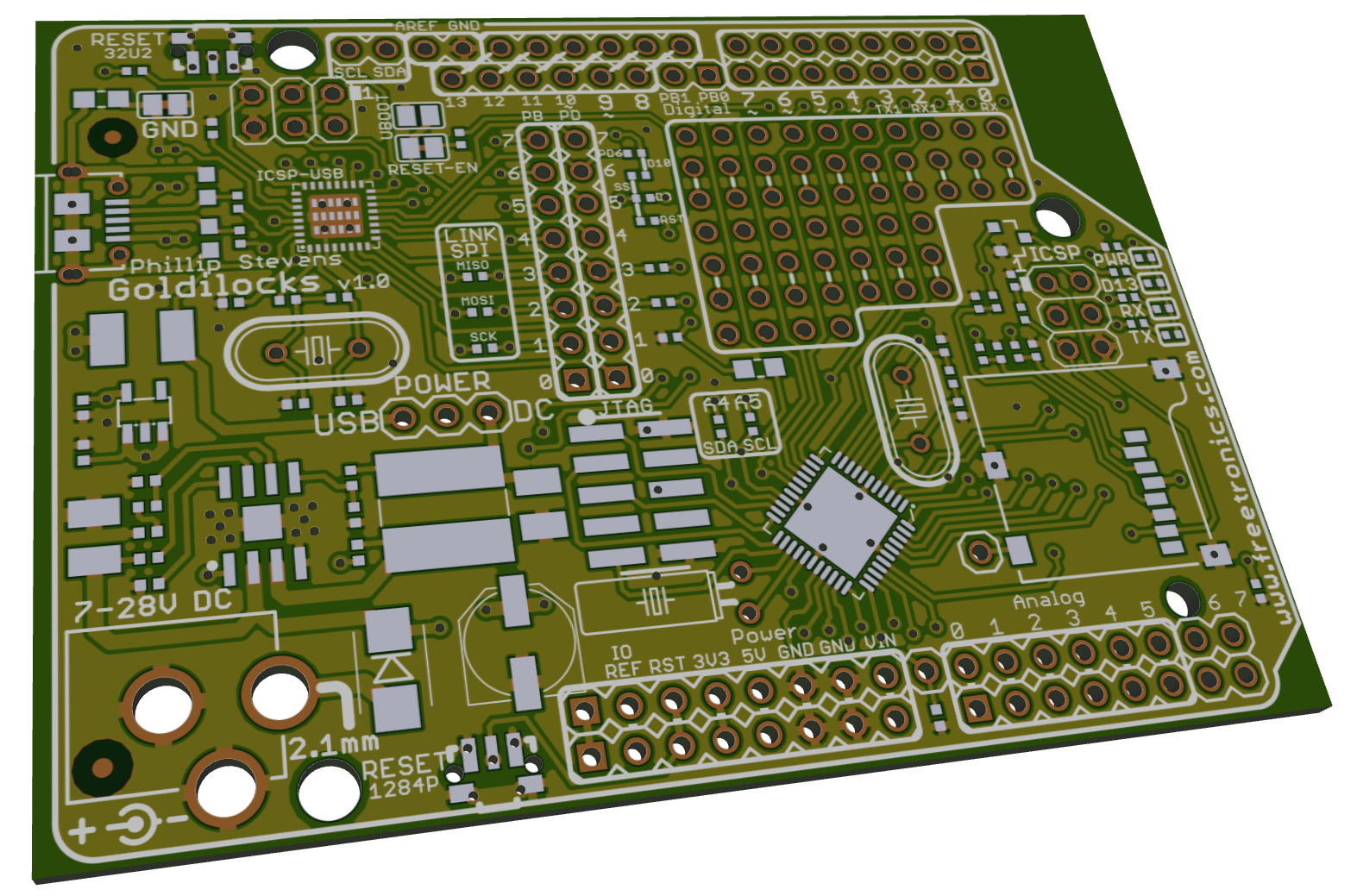
This is the Goldilocks v1.0 prototype.

This is a proposal to map the ATmega1284p pins to the Arduino physical platform.
| Arduino UNO R3 |
328p Feature | 328p Pin | 1284p Pin | 1284p Feature | Comment |
| Analog 0 | PC0 | PA0 | |||
| Analog 1 | PC1 | PA1 | |||
| Analog 2 | PC2 | PA2 | |||
| Analog 3 | PC3 | PA3 | |||
| Analog 4 | SDA | PC4 | PA4 | PC1 I2C -> Bridged | |
| Analog 5 | SCL | PC5 | PA5 | PC0 I2C -> Bridged | |
| Reset | Reset | PC6 | RESET | Separate Pin | |
| Digital 0 | RX | PD0 | PDO | RX0 | |
| Digital 1 | TX | PD1 | PD1 | TX0 | |
| Digital 2 | INT0 | PD2 | PD2 | INT0 / RX1 | Xtra USART1 |
| Digital 3 | INT1 / PWM2 | PD3 | PD3 | INT1 / TX1 | Xtra USART1 |
| Digital 4 | PD4 | PD4 | PWM1 | 16bit PWM | |
| Digital 5 | PWM0 | PD5 | PD5 | PWM1 | 16bit PWM |
| Digital 6 | PWM0 | PD6 | PD6 | PWM2 | |
| Digital 7 | PD7 | PD7 | PWM2 | ||
| Digital 8 | PB0 | PB2 | INT2 | Xtra External Interrupt -> ATmega32u2 x-pad |
|
| Digital 9 | PWM1 | PB1 | PB3 | PWM0 | |
| Digital 10 | SS / PWM1 | PB2 | PB4 | SS / PWM0 | SPI -> ATmega32u2 x-pad |
| Digital 11 | MOSI / PWM2 | PB3 | PB5 | MOSI | SPI |
| Digital 12 | MISO | PB4 | PB6 | MISO | SPI |
| Digital 13 | SCK | PB5 | PB7 | SCK | SPI |
| (Digital 14) | PB0 | -> SDCard SPI SS | |||
| (Digital 15) | PB1 | -> SDCard Card Sense | |||
| SCL | PC0 | SCL | I2C – Separate | ||
| SDA | PC1 | SDA | I2C – Separate | ||
| PC2 | TCK | JTAG | |||
| PC3 | TMS | JTAG | |||
| PC4 | TDO | JTAG | |||
| PC5 | TDI | JTAG | |||
| XTAL1 | PB6 | PC6 | TOSC1 | Unused | |
| XTAL2 | PB7 | PC7 | TOSC2 | Unused | |
| (Analog 6) | PA6 | Unused -> Pad / Hole | |||
| (Analog 7) | PA7 | Unused -> Pad / Hole |
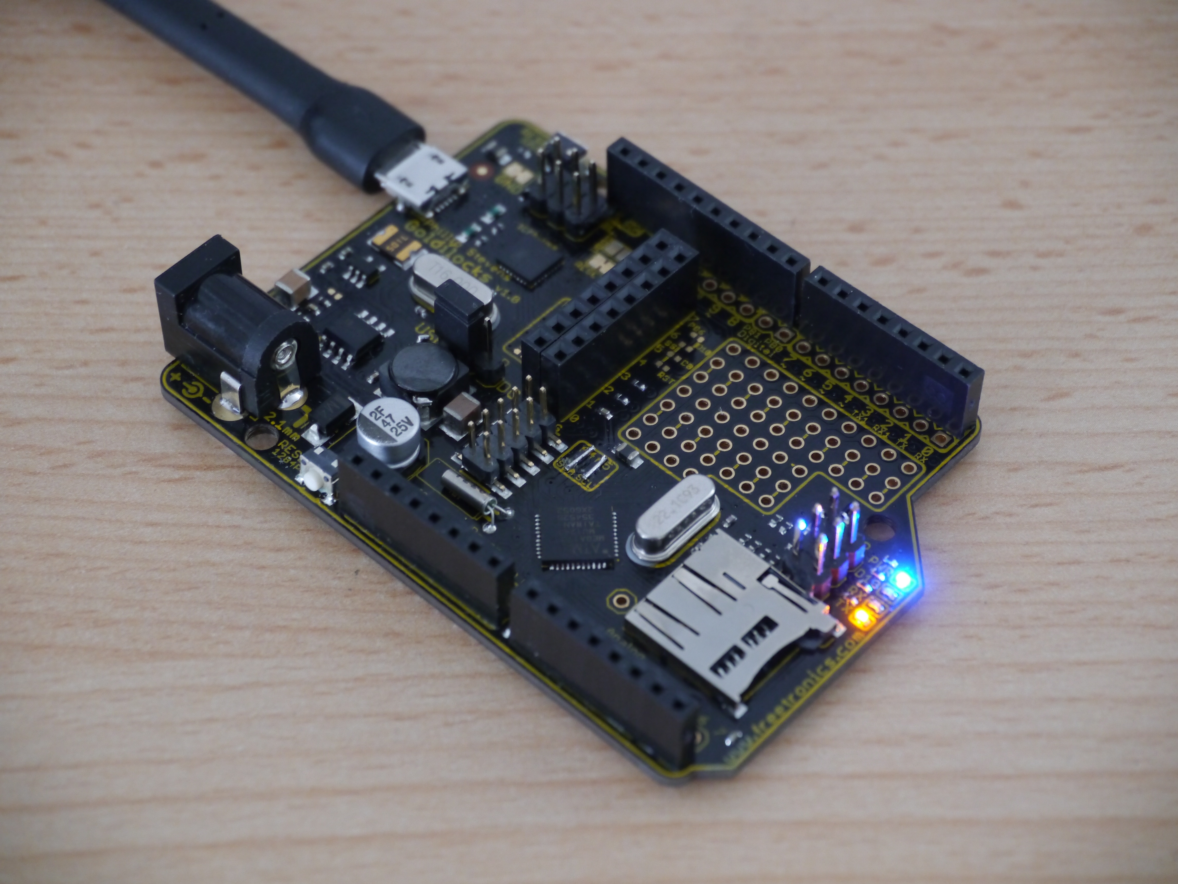
Here’s a picture of one of the two prototype boards, where I have added some additional items. I have changed the 1284p crystal to 22.1184MHz, and added a 5ppm 32kHz watch crystal for testing the avr-libc provided time.h functions.
Also I added header sockets for the 32u2 so that I could test its ability to program the 1284p using the LUFA AVRISP code, and determine how much decoupling should be added to the SPI bus link option. This is to ensure that even if the SPI bus is linked between the two MCU, that the 32u2 can’t lock up the SPI bus for devices trying to talk to the 1284p.
Also, I’ve added bridges for the SCL/SDA pins to the A4/A5 pins for old format (pre R3) shields.
I’ve prepared a preliminary distribution of the entire code set for goldilocks, including the lufa 130313 code used in the 32u2 and the stk500v2 bootloader used in the 1284p. This code is laid out in the arduino manner, with the directories matching the usual layout of Arduino boards.
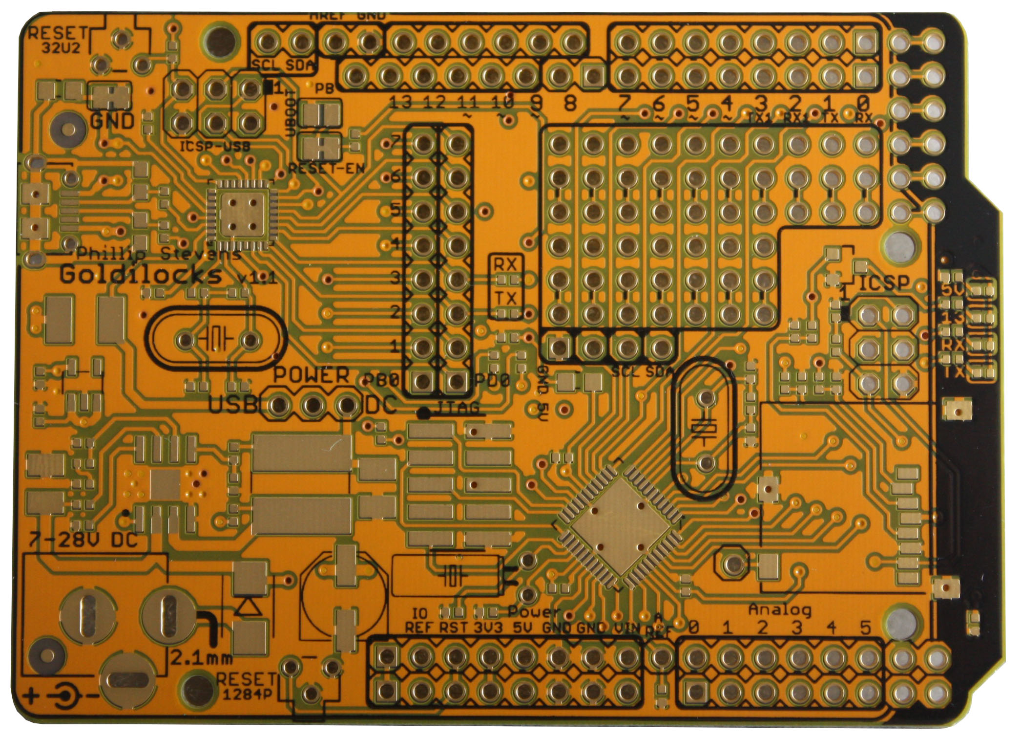
The production board design was finalised on June 28th and sent for manufacturing. The v1.1 production boards are shown below. Pick and place pictures soon.
Goldilocks v1.1 PCB Front
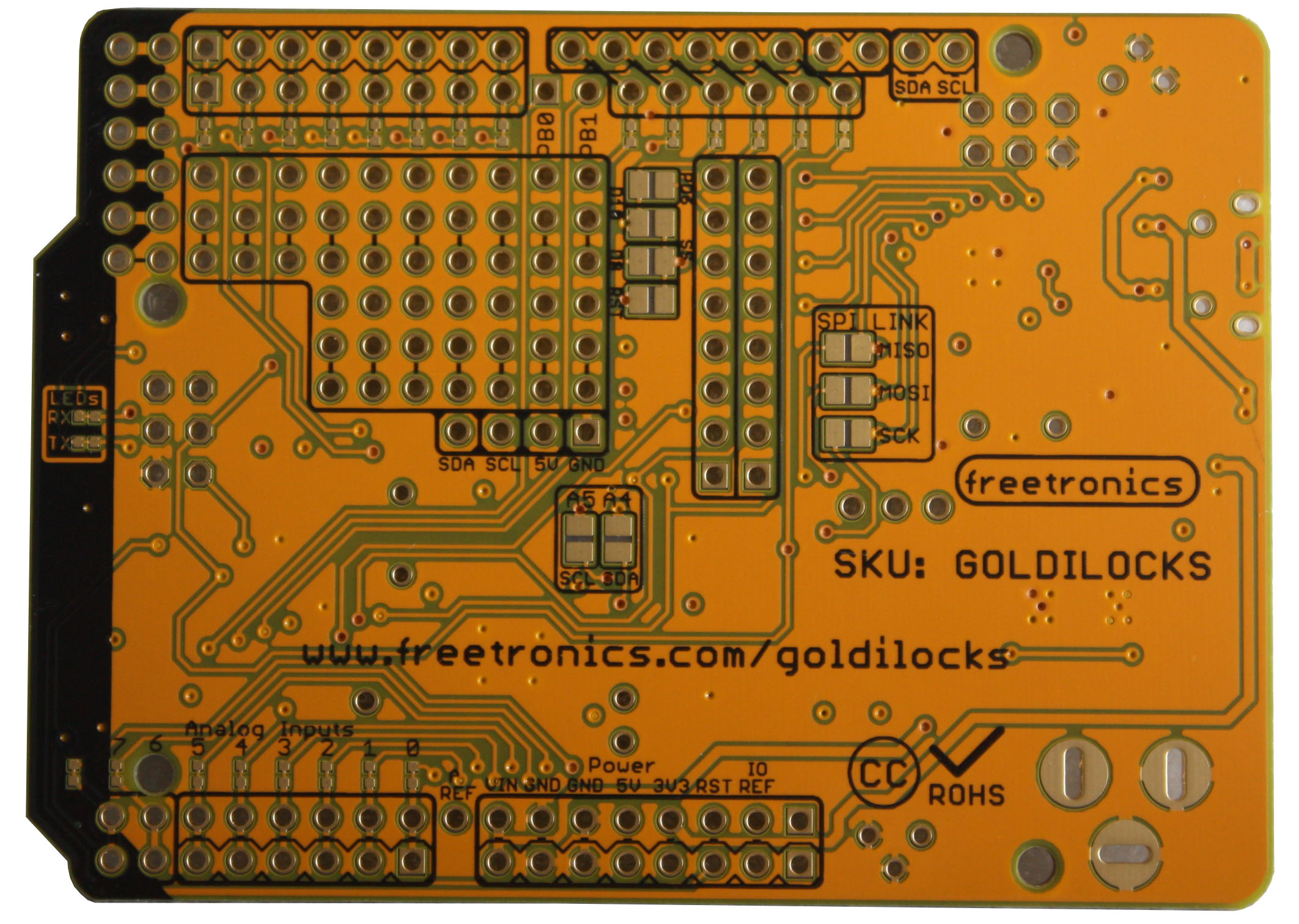
Goldilocks v1.1 PCB Back
Firmware
Moved support to the Arduino IDE Boards Manager.
Recompiled bootloader binaries with avr-gcc 4.9.2.
Returned to the original 2013 pins_arduino.h pin numbering, now that analogRead() issues are corrected.
Look for Goldilocks in the Unofficial Boards Support List, and follow the instructions in the Goldilocks Analogue User Manual.
Support for Arduino IDE 1.6.x.
Increased 1284p bootloader time out to 4 seconds.
Set upload speed to 38400 (single speed UART) for Goldilocks Analogue.
Support for Arduino IDE 1.5.x. Updated to LUFA 140928 for DFU and U2duino for 32u2.
No change for 1284p. Added Goldilocks Analogue bootloader, but no LUFA required because of FTDI USB interface.
Updated directory structure to support Arduino IDE 1.5.x. Modified pins_arduino.h to support analogRead() correctly.
Updated to LUFA 130901 for DFU and U2duino for 32u2. No change for 1284p.
Obsolete – Fixed USART mismatch by adjusting stk500v2 bootloader to 38,400 baud.
Obsolete – Fixed 32U2 tristate RESET issue.
Obsolete – Fixed stk500v2 bootloader monitor issues and included compiled firmware files.
Obsolete – Initial release.
