Introduction
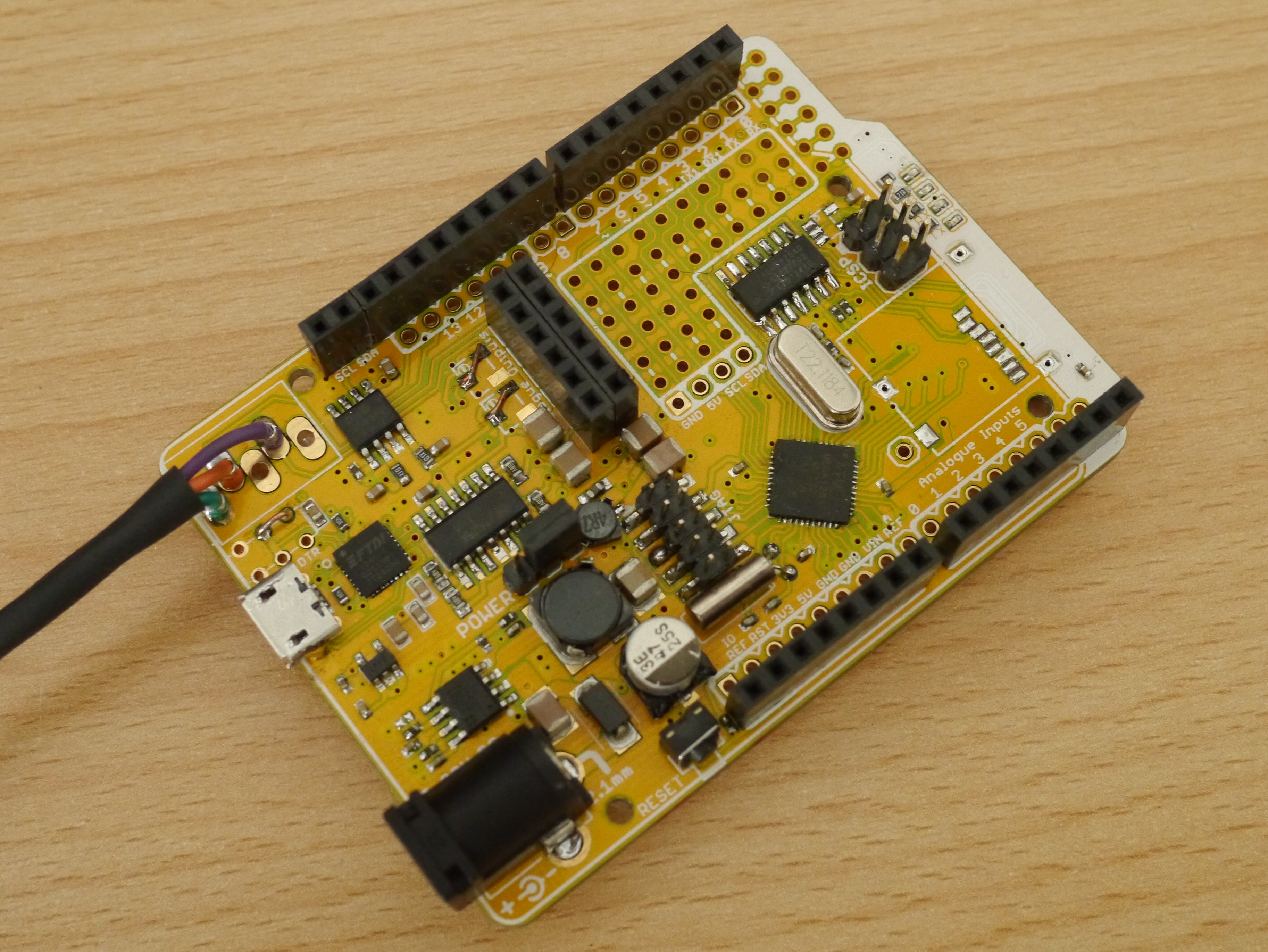
Following my initial design article, and the testing article, I’ve put quite a lot of thought into how I can make this Goldilocks Analogue device best achieve my stated goals. Pictured is the only Goldilocks Analogue Prototype in existence.

Goldilocks Analogue Prototype – Analogue section front of image.
From the testing it was clear that the MCP4822 DAC fully achieved the goals that I had set out to achieve, but that my design for the analogue buffer stage behind it was really quite bad. Fixing it was going to take some thought.
I have decided to separate the analogue output stage into two sections. An AC section which drives the headphone socket, with a designed for purpose headphone amplifier device, and a DC section using a high current rail to rail OpAmp and a negative 1.18V supply rail to allow the OpAmp to fully reach GND or the equivalent 0x000 digital input.
I also found a better solution for the uSD level translation. There is a device designed for purpose, which I’ve now designed into the Goldilocks Analogue.
DAC – MCP4822
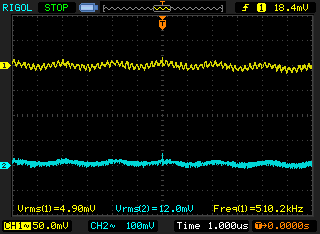
The selected dual DAC uses the SPI bus to write 12 bit values to each of its channels. The increments are either 1mV or 0.5mV giving full scale at DC 4.096V or 2.048V depending which scale factor is being used. The testing showed that the DAC is capable of achieving close to the 72dB of SNR that is its theoretical capability.
So from my point of view the DAC, and the AVcc filtering system employed to provide a clean analogue power rail, have achieved their design goal. Let’s not change anything.
Headphone (AC) Output – TPA6132A2
Driving a headphone socket with a nominal impedance of 32 ohm is a hard job for an OpAmp, and they are not designed specifically for this job. Therefore, I thought it would be best to separate the two outputs into two separate full-time output devices, specialised for their purposes (AC headphones, and DC PID or general pin-out). Both Goldilocks Analogue output options are driven simultaneously, and they will not interfere with each other.

For the AC and headphone output, using a specific single ended “DirectPath” headphone amplifier device enabled me to remove the large output coupling capacitors but still achieve a good low frequency output response.
The TPA6132A2 is capable of driving 25 mW into 16 ohm headphones. Its amplifier architecture operates from a single supply voltage and uses an internal charge pump to generate a negative supply rail for the headphone amplifier. The output voltages are centred around 0 V and are capable of positive and negative voltage swings. This means that the TPA6132A2 doesn’t need output blocking capacitors, and therefore can achieve a very good low-frequency fidelity. Using the 1 uF input capacitors stops any turn-on pop or noise, and achieves a low frequency corner below 10 Hz.
As the DAC outputs a signal with up to 4 V peak to peak, I have set the gain on the TPA6132A2 to -6dB. This should result in the full range of the headphone signal being 1 V peak to peak, with approximately 25 mW being delivered into 32 ohm headphones.
The TPA6132 also has a very high power supply an RF noise rejection ratio. Although I’ve gone to a lot of effort to filter the AVcc power supply, the power supply noise generated was still significant. Having over 90 dB PSRR will help to keep the output quiet.
Analogue (DC) Output – TS922A
I originally selected a highly regarded audiophile OpAmp for use in the Goldilocks Analogue. That device was incapable of operating close to its GND rail, and caused significant distortion in the output signal. Based on that experience, I decided to use a rail-to-rail output OpAmp to provide the DC buffered signal.
Even though rail-to-rail OpAmp devices are sold as full Vcc to Vss outputs, under high current loading they all have significant output droop. The only way to avoid this is to avoid driving the (any) OpAmp close to its supply rails.
The positive rail is ok. The supply voltage is a well regulated 5 V DC, and the maximum voltage required from the OpAmp is 4.096 V which is 0xFFF input to the DAC. It is the Ground Rail, which causes the issue, as the OpAmp will be unable to deliver the analogue equivalent 0x000 under high current situations.
The only way to get an OpAmp to deliver a solid GND potential output, is to supply it with a negative supply voltage Vss. Getting a Vss rail is described below.
The TS922A device is designed for high current rail-to-rail outputs, and is specified to work into 32 ohm headphones, 75 ohm video, and 600 ohm inputs. This DC coupled output can be used to drive PID, Triac or any other application requiring a precise analogue signal up to around 50 kHz.
OpAmp Vss (negative) rail
The TS922A can support over 50 mA per channel output, but at this current its output resistance has dropped its ability to reach both rails to greater than 300 mV. Specifically, it can only reach between 0.3 V and 4.4 V. Therefore to enable the output signal to reach GND potential, we have to generate a Vss with greater than -0.3 V, and capable of supplying in excess of 100 mA (over OpAmp both channels).
I looked at a number of options for charge coupled devices, and decided that the cheapest and best way was to use two paralleled TPS60403 devices to each generate -5 V 60 mA from the 5V power rail. These devices don’t filter their output, but since we are not going to use the -5 V directly, this doesn’t matter.

Following the generation of the -5 V supply, I’ve decided on a TPS72301 variable voltage 200 mA linear regulator, configured to generate its reference voltage -1.186 V, to provide a regulated Vss. Using the internal reference voltage saves a few resistors, and it still generates sufficient negative voltage to enable the OpAmp to easily reach true GND potential.
uSD Card Level Translation – TXS0104
Some further analysis of the voltage translation application revealed that the TXS0104 is designed to exactly suit the purpose of interfacing SPI bus at up to 24 MHz. As a side benefit it is a much smaller package, which recovers prototyping space back to the original Goldilocks benchmark. It is also cheaper than the general purpose OpAmps previously used.
Initially, the prototype used the TXB0104 device, but it was unsuccessful. The 4kOhm output resistance combined with less than optimal uSD card characteristics meant that the design failed. The TXB series cannot drive anything with pull-up or pull-down greater than 50kOhm. The uSD card is specified to have 10kOhm to 100kOhm integrated pull-up resistors, but in practice they all seem to be around 10kOhm. The schematic below will be updated to show TXS shortly.

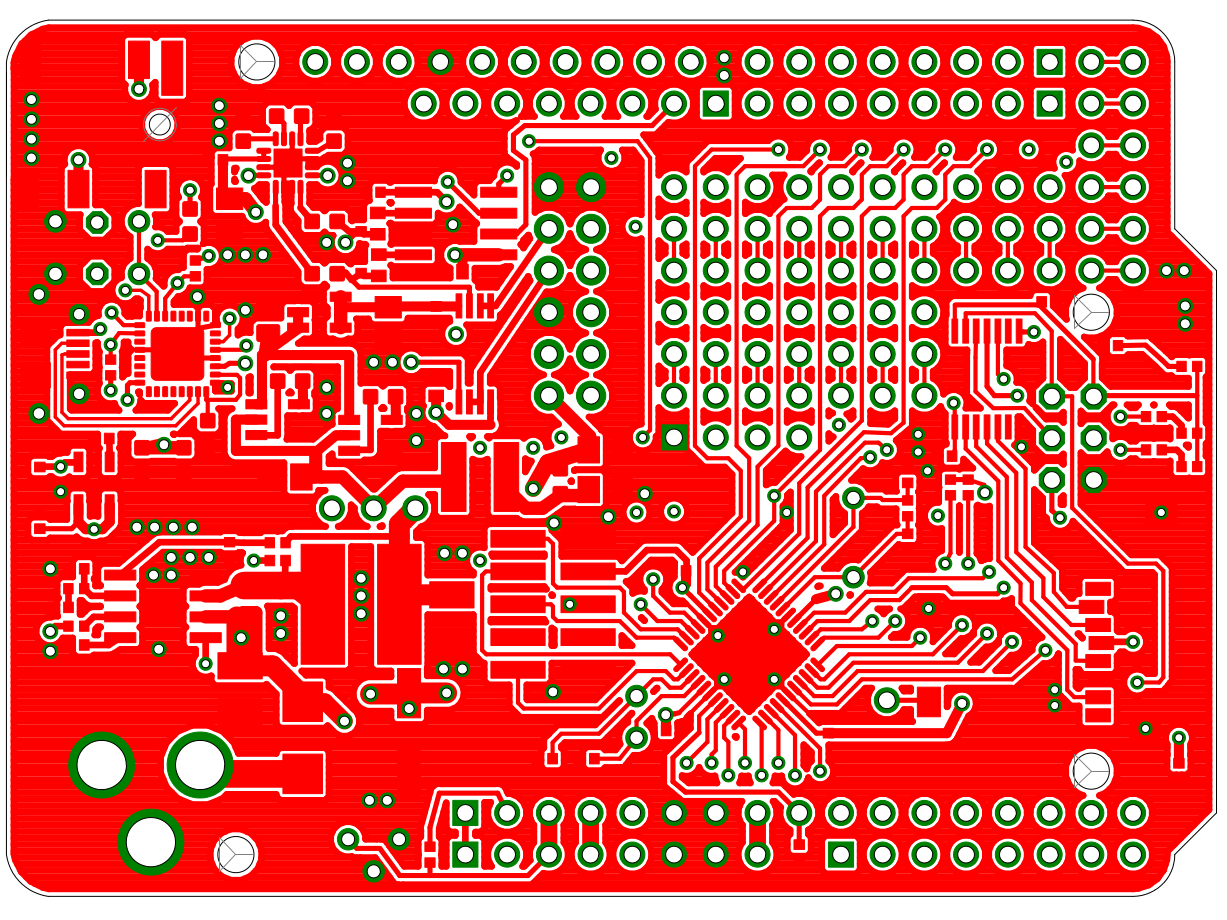
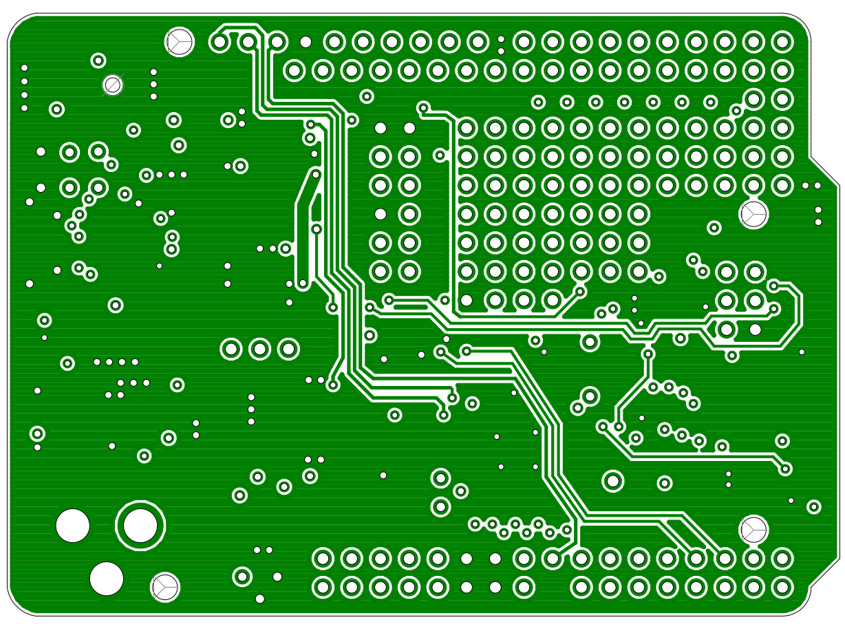
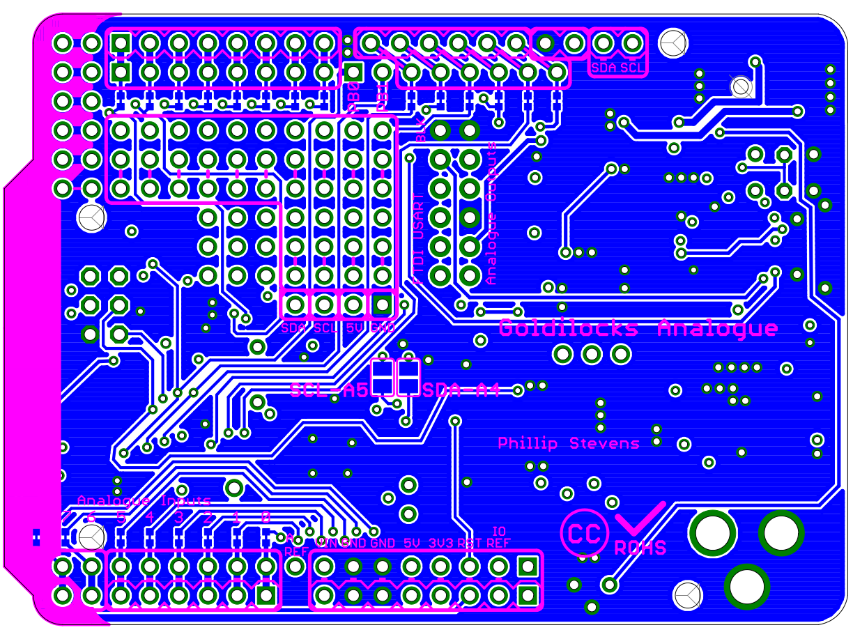
The PCB Layout
The board layout has been completed, and a PCB ordered to this design.
More detail soon.
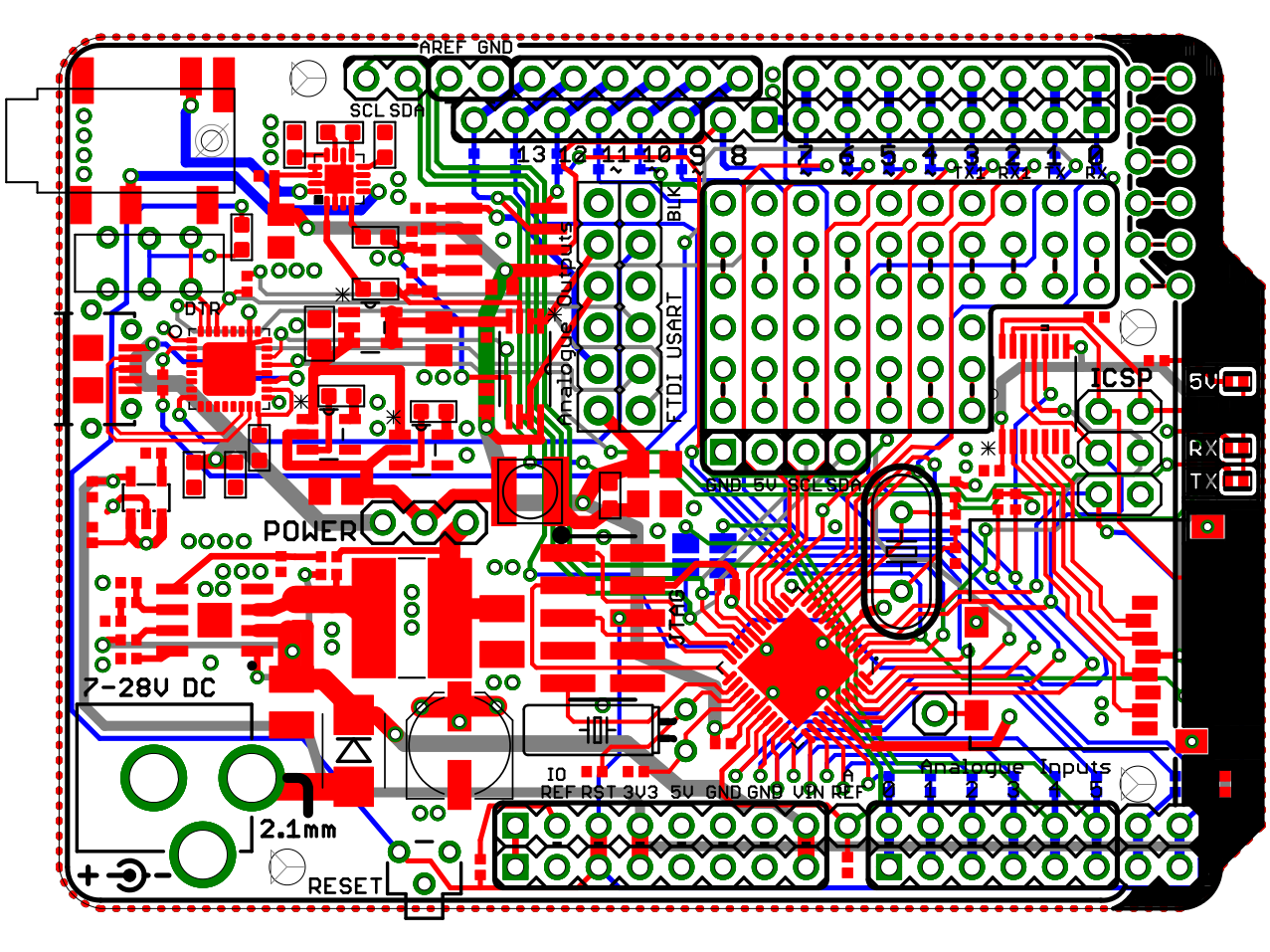
Top Signal Layer
GND Signal Layer
5V Signal Layer

Bottom Signal Layer
As of June 2014, I’ve now got all the parts, and the PCB ready for a new prototype. This new version was constructed late July 2014 and is awaiting basic testing.

Version 2 of the prototype, fresh out of the oven.
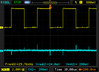
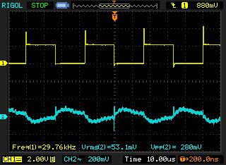
As of August 2014, I have started testing. So far the analogue design seems to check out, with both the headphone (AC biased) circuitry and the OpAmp (DC biased) circuitry performing as intended. More testing soon, and a new post.
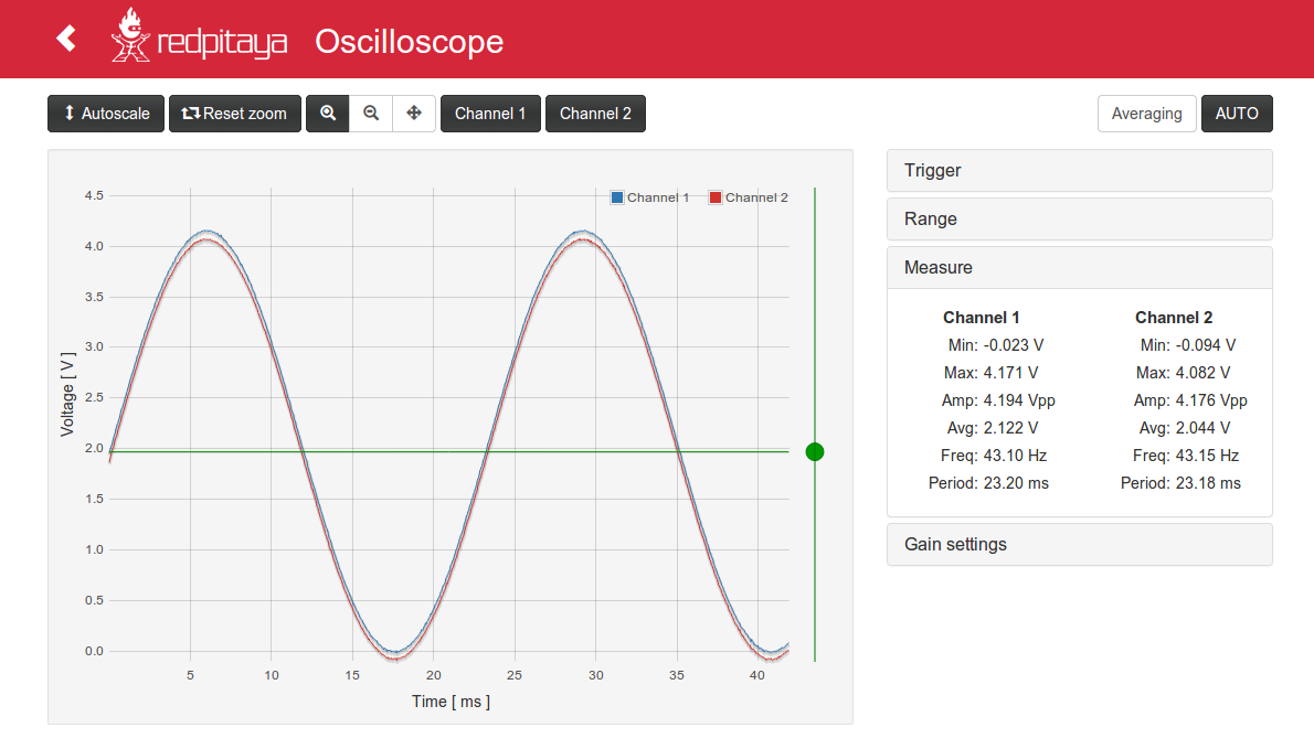
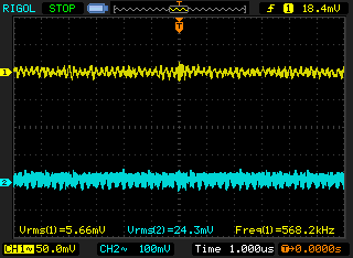
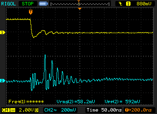
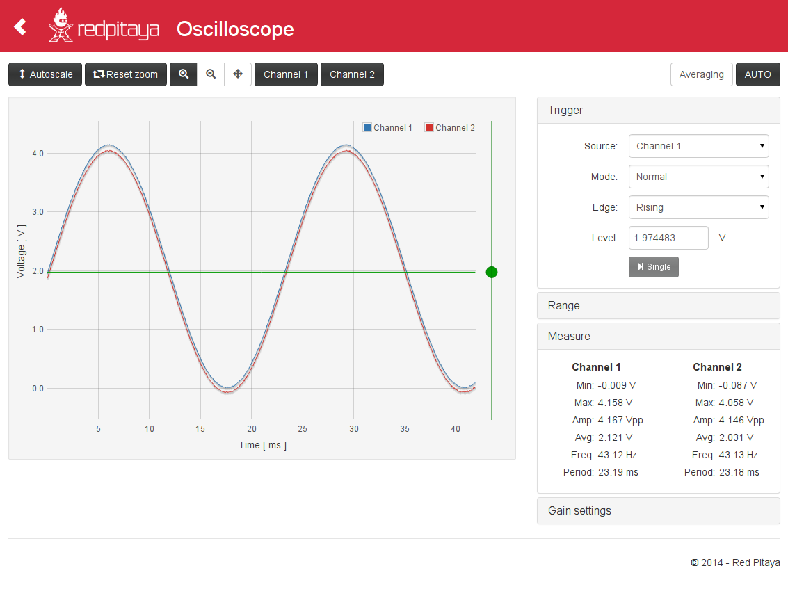
Goldilocks Analogue demonstrating a clean DC biased sign wave (to 0V) .
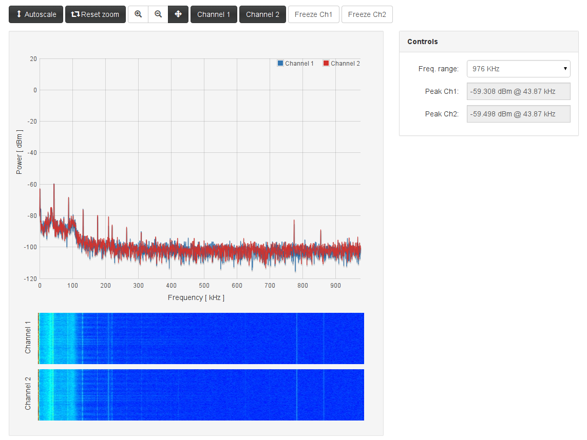
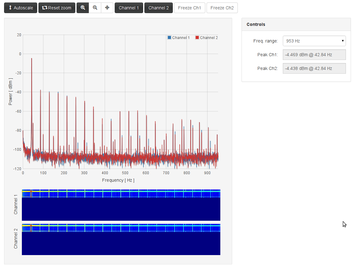
The spectrum at the output of the TS922A OpAmp is cleaner now than directly at the MCP4822 DAC output of the previous prototype iteration.
The nominal 12 bit DAC capabilities are able to achieve 72dB SNR. Target achieved.
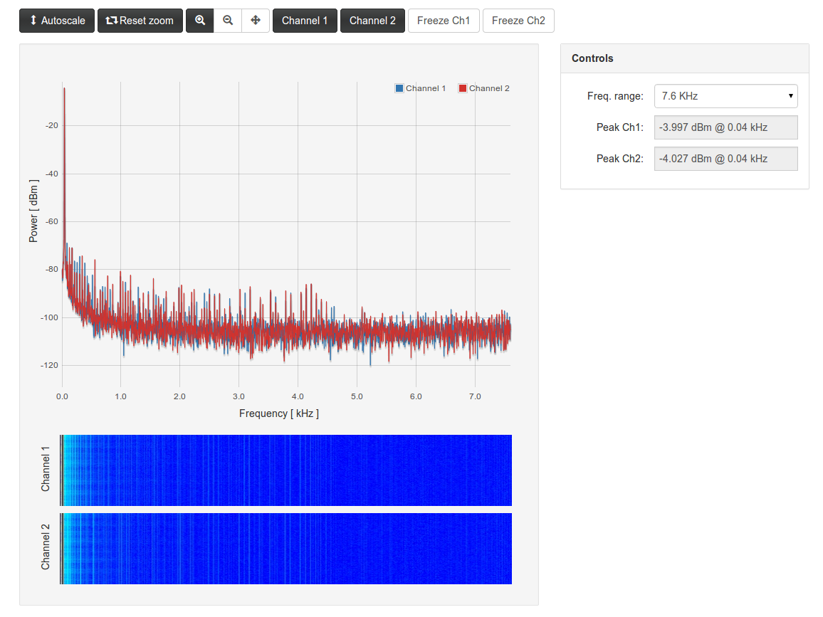
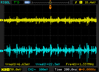
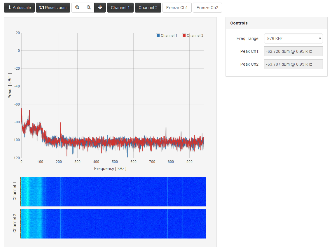
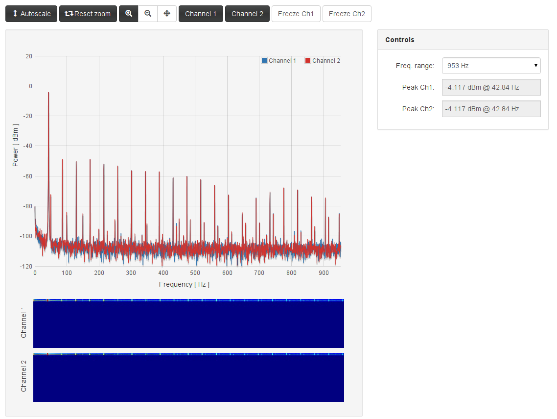
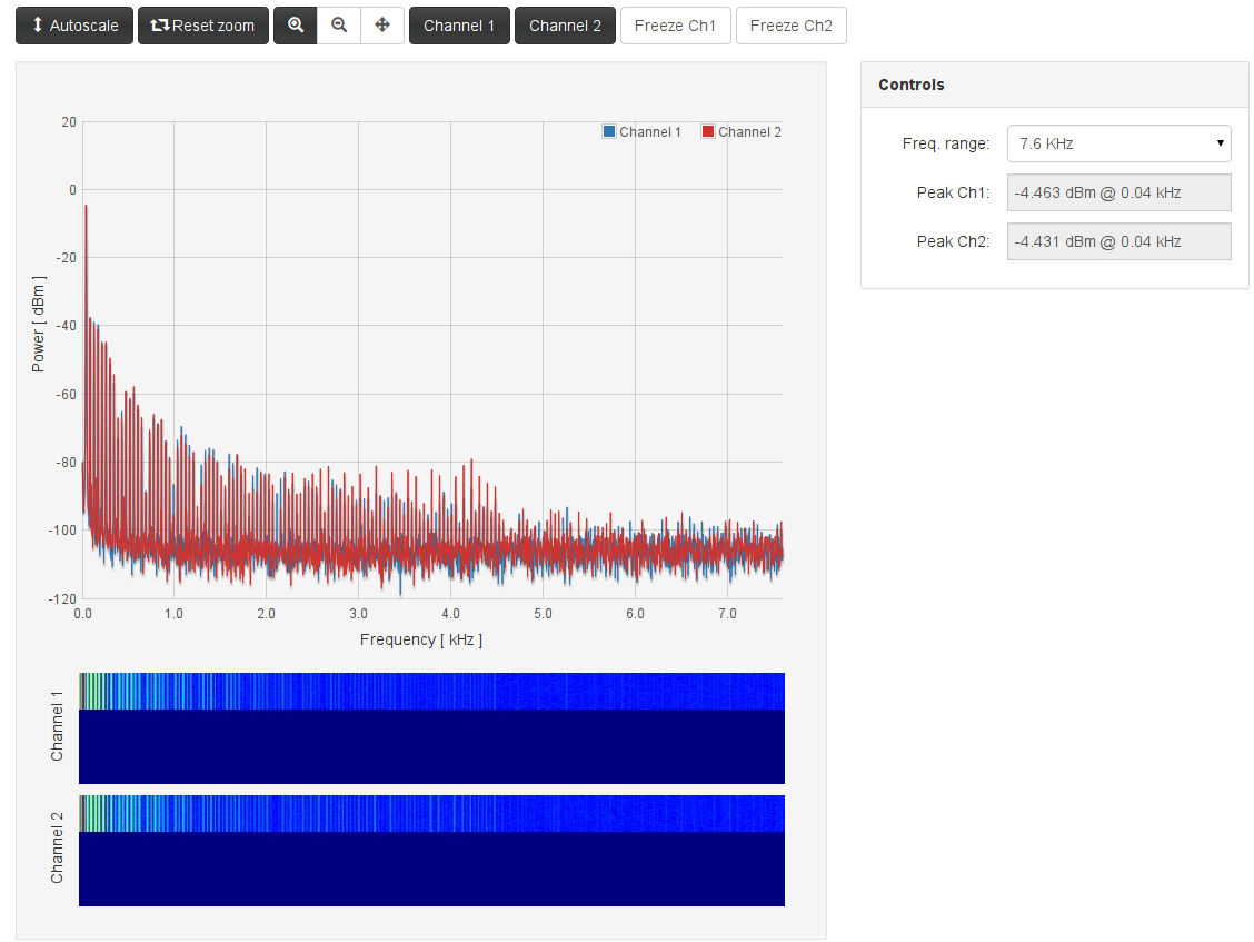
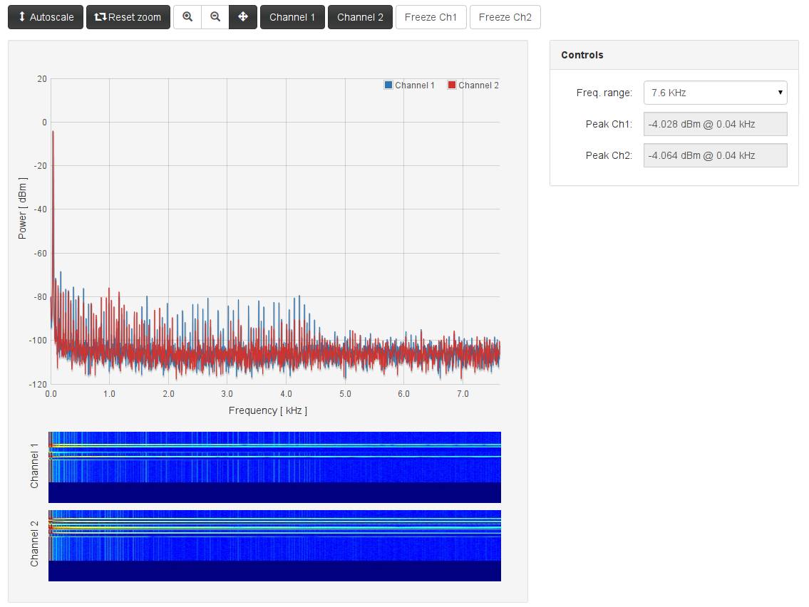
Spectrum at the output of the OpAmp.