CP/M-IDE for RC2014

Just over 4 years ago, on 18th March 2018, I committed the first CP/M-IDE files into the RC2014 repository. Now that some time has passed and it has developed into a stable solution for CP/M I think it is time to fill in some details about why it was written, how it differs from other CP/M implementations, and how to reproduce images to match those in the CP/M-IDE repository.

Concept

There are several implementations of CP/M available for the RC2014. Initially, the CP/M on a Breadboard project implemented by Grant Searle became the default implementation for the Z80 RC2014. Slightly later Wayne Warthen added support for the RC2014 to the Z80/Z180 RomWBW System. RomWBW is a very extensive and advanced set of system software, supporting many different RetroBrew machines, and in general it requires 512kB ROM and 512kB RAM to reach its full potential.

Each of these implementations has its own focus. The 9 Chip CP/M is based on simplicity, and being able to be built on a breadboard with the minimum of complexity, but it has not been maintained (e.g. correcting the bugs in the SIO and ACIA serial implementations requiring arbitrary interstitial delays to be inserted, otherwise data loss occurs) and it has a substantially smaller TPA. Alternatively, RomWBW supports a variety of hardware including Z180 CPUs, and provides an underlying generalised architecture support which provides paged memory and many facilities but this imposes a processing overhead on I/O, and requires substantially more RAM (512kB) than a typical CP/M system.

Faced with both these options, and being very interested to build my own solution, and to use my growing experiences supporting the z88dk community, I decided to build CP/M-IDE to fulfil a specific niche.

The CP/M-IDE is designed to provide support for CP/M on Z80 while using a normal FATFS formatted PATA or IDE drive. And further, to do so with the minimum of cards, complexity, and expense. Most recently, it has also become the CP/M which supports the 8085 CPU Module. Also recently, support for the standard RC2014 Pro with CF Module v2.0 and for the RC2014 Mini II with CP/M Expansion Kit has been added.

Initially I chose the IDE Hard Drive Module specifically because I could use it to attach any old hard drive, aka “spinning rust”, to my RC2014, and this led to support for everything from these old 3 1/2″ hard drives, through to modern SSD or DOM solid state drives. It also supports both old and modern high capacity Compact Flash Cards in their native 16-bit mode, so readily available modern 1 and 2 GigaByte Compact Flash cards are OK. It is also possible to use SD Card to CF Card adapters with the IDE Hard Drive Module or the CF Module v2.0, allowing direct support of modern pluggable SD or Micro SD storage.

I also wanted to build a very inexpensive system so the original RC2014 Pro with CF Module v2.0, or RC2014 Mini with CP/M Expansion Kit, is sufficient for modern storage solutions. And as an option the RC2014 IDE Hard Drive Module is the only additional Module required to operate CP/M-IDE with older “spinning rust” hard drives. It is NOT necessary to buy an expensive 512kB/512kB Memory Module as the standard 64kB RAM Memory Module works fine. If there’s no need or interest to attach proper IDE hard drives, or using a Compact Flash Module for storing CP/M drives is preferred, then there is no additional hardware required over the RC2014 Pro standard product.

CP/M is a very compact Operating System and, in the most common version 2.2, it supports only serial interfaces and disk interfaces. For the RC2014 there are two standard serial Modules, being the ACIA Module (used in the RC2014 Mini) and the more advanced and expensive SIO/2 Module (used in the RC2014 Pro).

As I’m quite interested in building real-time and event driven systems, in contrast to other CP/M implementations, CP/M-IDE therefore includes drivers supporting both transmit and receive interrupt based solutions, sourced from my z88dk RC2014 support package for the ACIA serial interface and the SIO/2 serial interface.
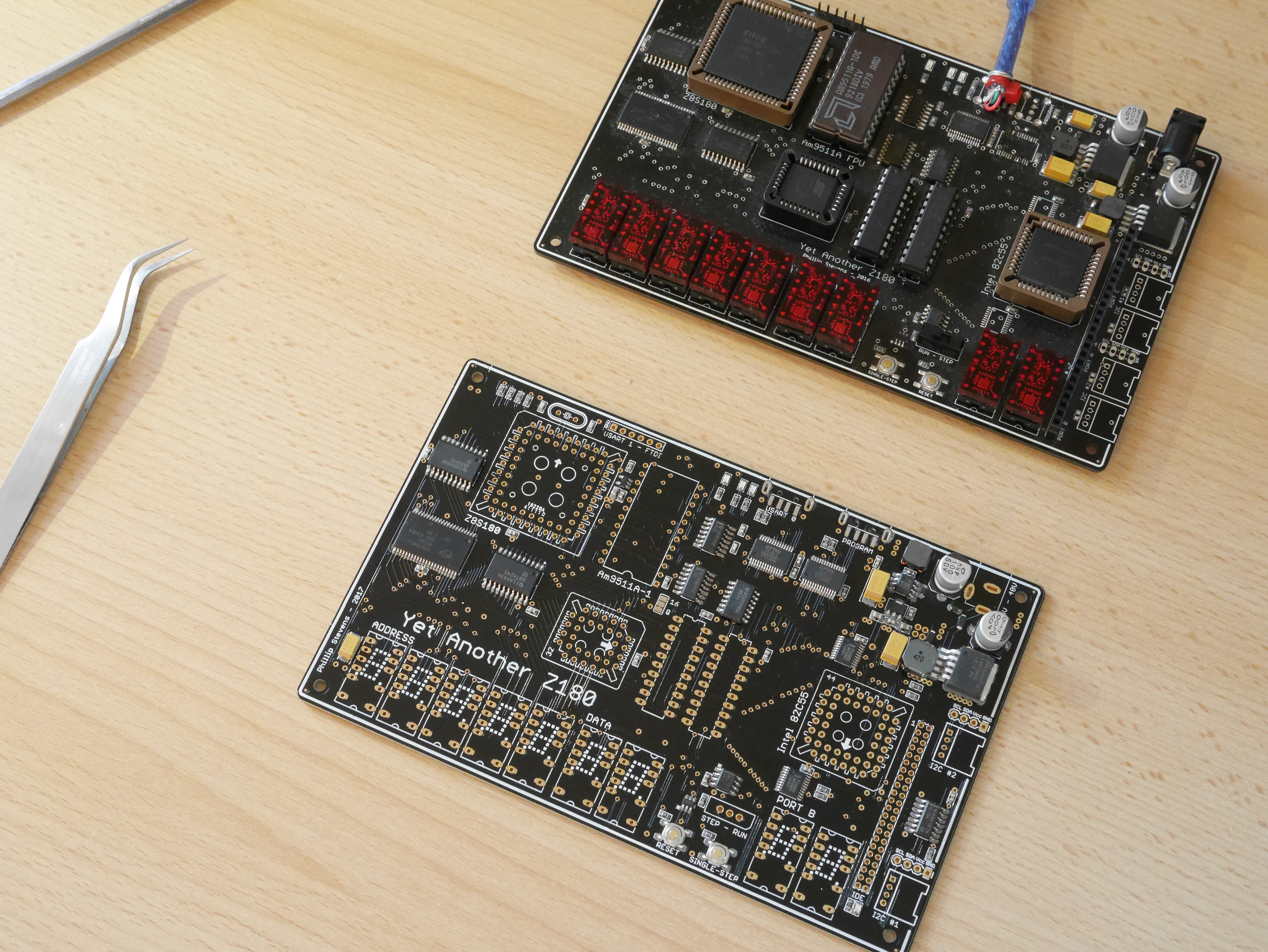
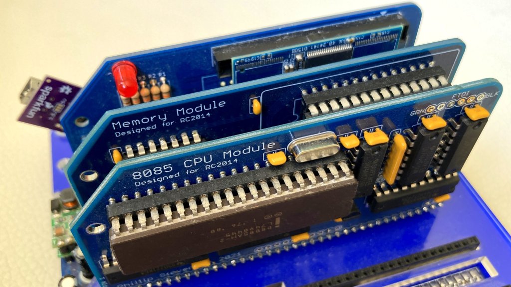
8085 CPU Module

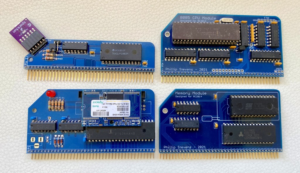
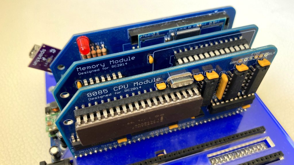
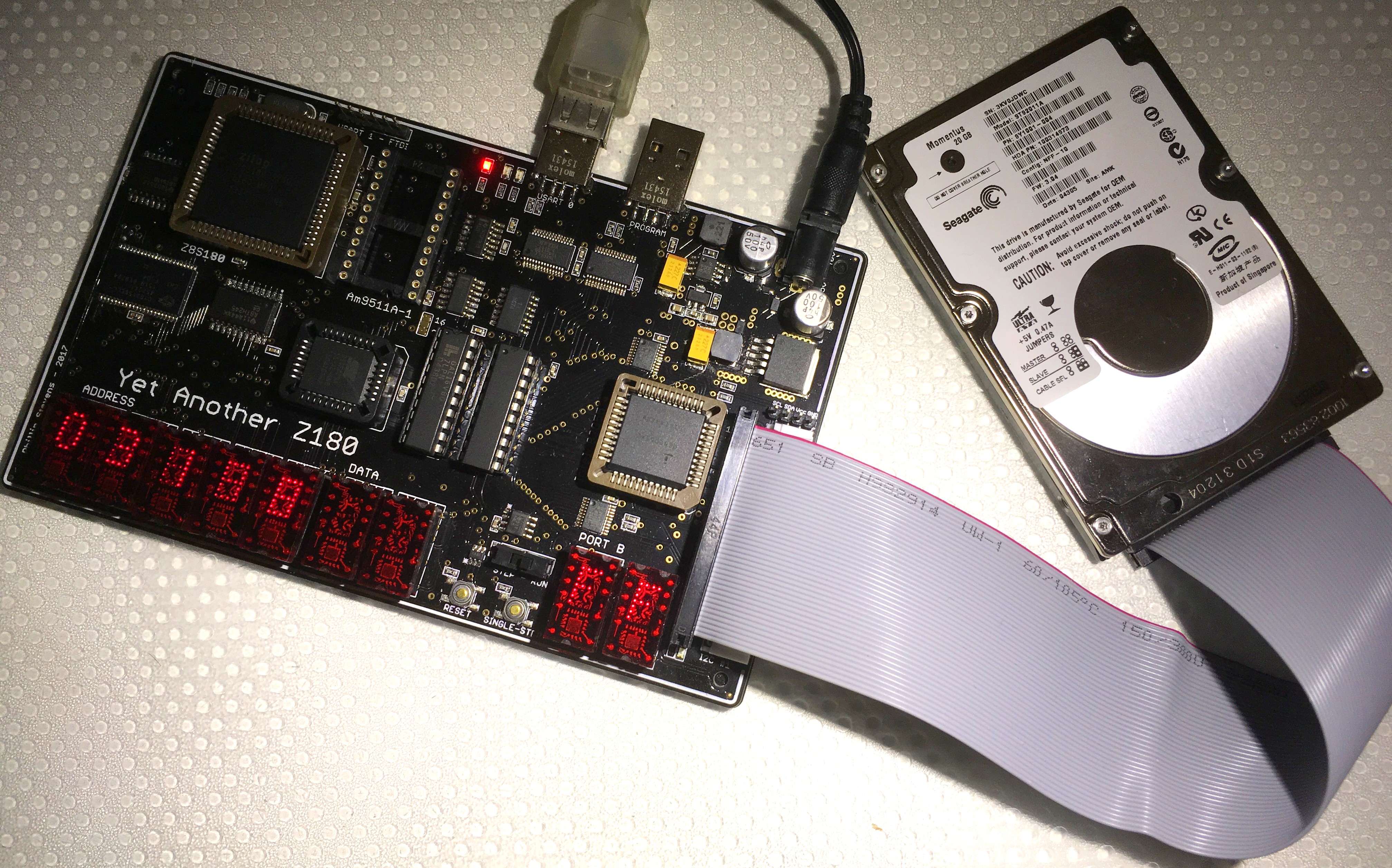
More recently I have built a 8085 CPU Module for the RC2014 System. This is the first time that an 8085 CPU has been integrated into the RC2014 System, and it is able to work with the Z80 bus signalling required to drive the standard RC2014 Modules.

CP/M-IDE 8085 RC2014 System

I am very pleased to have a wholly Intel RC2014 System equipped with the 8085 CPU Module, the 8231A APU Module, and the 8255 IDE Module. This is the original “Intel Inside”, before it became marketing jargon.

Hardware

The concept remains to use the minimum of additional hardware over the entry level RC2014 Pro model. In fact just the IDE Hard Drive Module is desirable. But, the standard CF Module v2.0 (and derivatives) can also be used as it supports modern (large capacity) CF Cards, and the RC2014 Mini II with CP/M Expansion Kit is also supported.

IDE Hard Drive Interface

The IDE Hard Drive Module is based on the 8255 PPI device. This device was designed to work with the 8085 CPU and 8086 CPU. It is perfectly suited to supporting a 16-bit parallel IDE interface as it provides latching of signals on 3 separate 8-bit ports.

Initially I was concerned that the selection of control signal pins for the IDE interface limited the possibility for use of the 82C55 device for generalised I/O. I still think that this is an issue but, since no one has implemented further generalised solutions, the point is moot.

The IDE Hard Drive Module supports PATA hard drives of all types (including SSD IDE and DOM storage) and Compact Flash Cards and SD Card Adapters in native 16-bit PATA mode with buffered I/O being provided by the 82C55 device.

The IDE interface (or also termed diskio) is optimised for performance and can achieve over 110kB/s throughput using the FatFS library in C. It does this by minimising error management and streamlining read and write routines. The assumption is that modern IDE drives have their own error management and if there are errors from the IDE interface, then there are bigger issues at stake.

The CF Module interface can achieve over 200kB/s throughput at FATFS level, and seems to provide best performance using SD Cards in SD Card to CF Card Adapters. The old default RC2014 CF Module v1.3 is often unstable with modern CF Cards or with SD to CF Card Adapters. However the recent RC2014 CF Module v2.0 has become quite reliable with all modern large and small CF Cards. If you experience problems, then seek out this recent implementation.

For both IDE interfaces, within CP/M performance is approximately half the FATFS performance because the CP/M deblocking algorithm implements a double buffer copy process where 512 Byte physical sectors found on IDE disks are converted into the 128 Byte logical disk blocks that CP/M expects.

Serial Interfaces

In the ACIA builds, the receive interface has a 255 byte software buffer, together with an optimised buffer management supporting the 68C50 ACIA receive double buffer. The choice of memory size for the receive buffer is based on optimisations available by having the buffer a full “page”. Also text can be “pasted” in fairly large chunks into the CP/M command line without losing bytes.

Hardware (RTS) flow control of the ACIA is provided. The ACIA transmit interface is also buffered, with direct cut-through when the 31 byte software buffer is empty, to ensure that the CPU is not held in wait state during serial transmission. The size of the transmit interface buffer is based on free memory within the CP/M BIOS. As BIOS memory is typically reserved to start on the 256 Byte page boundary, if an update needed to consume more RAM, I would reduce the size of the transmit buffer to avoid the need to consume an additional page of BIOS memory.

In the SIO/2 build, both ports are enabled. Both ports have a 127 byte software receive buffer supporting the SIO/2 receive quad hardware buffer, and a 15 byte software transmit buffer. The transmit function has direct cut-through when the software buffer is empty. Hardware (RTS) flow control of the SIO/2 is provided. Full IM2 interrupt vector steering is implemented.

As both ACIA and SIO/2 devices have a hardware buffer for received bytes, it is important for the receiving interrupt handler to drain these buffers completely before returning execution to the program. If this is not done there is a danger that received bytes could be overrun and lost.

For the CP/M-IDE 8085 build the Serial Output (SOD) FTDI interface found on the 8085 CPU Module is enabled as the CP/M LPT: interface. This is activated by using ^p as per normal practice.

Additional Hardware

Whilst there is no support for additional hardware within CP/M itself (as there are no BDOS calls standardised), it is possible to use additional hardware in CP/M applications. Typical hardware options include the APU Module, various Sound Modules, and digital I/O Module.

CP/M Implementation

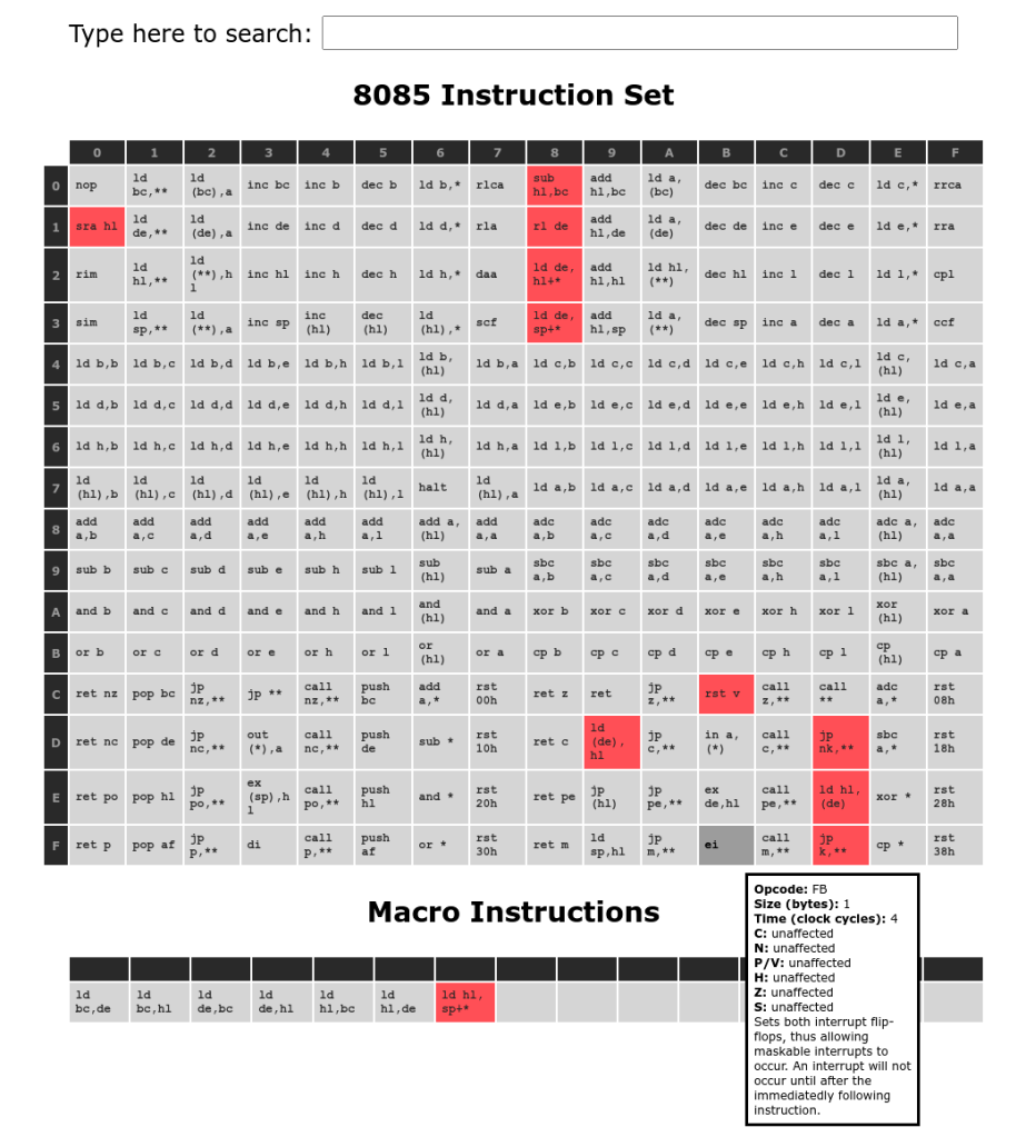
There are many descriptions of Digital Research CP/M, so I won’t go into detail. It is important to know that CP/M v2.2 was in its day the most widely deployed Operating System for small computers based on the 8080, 8085, and Z80 CPUs. Later versions of CP/M supported the 8086, and 68000 CPUs, as well as providing many more system functions than the CP/M v2.2.

Whilst there have been later versions of CP/M produced, to my knowledge, there were no widely available user applications produced which could not be run on CP/M v2.2. This broad compatibility is why CP/M v2.2 is important.

CP/M v2.2 is essentially just 4 pieces of code. The BIOS (Basic Input Output System) is provided to abstract the hardware devices from the operating system. Essentially there is a limited set of BIOS commands that the BDOS can call on. These BIOS commands are implemented specifically for the characteristics each machine, and in the early days of computing it was essential that a user knew how to write their own BIOS.

The second piece of code is the Page 0 of memory, which is written by the BIOS cold boot command on initialisation. The role of this Page 0 is to provide important addresses (for both BIOS and BDOS) and to set important status registers like the I/O Byte. The Page 0 is also used to manage the 8080, 8085, and Z80 CPU interrupt vectors, and to store the command line entered by the user when an application is initialised.

The CP/M BDOS is the middle layer of the Operating System. Application programs rely on BDOS system calls to support their requirements. Here the drives (A:, B:, through to maximally P:) are opened and closed, and disk sectors are written. The BDOS does its work by calling BIOS commands on behalf of the application that is currently loaded.

Often the BDOS is combined with the CCP (Console Command Processor) into one assembly language file because both of these components are constant and they are independent of the hardware. These two components are essentially the distribution of Digital Research CP/M which was sold to the user.

The CCP is the user interface for CP/M. It provides a very small number of integrated commands, like “directory list”, “erase”, “rename”, “type” or “exit”, but its main role is to load additional commands or applications called “Transient Programs” into RAM and execute them. Often, an application loaded into the Transient Program Area (TPA) RAM will overwrite the CCP in memory as it is normal for the CCP (and BDOS) to be reloaded once an application quits.

There are third-party alternatives available for both the CCP and BDOS, and as these are loaded each time the computer is restarted it is possible to replace the default versions by alternatives if desired. Specifically for CP/M-IDE, the DRI CCP can be replaced by Microshell SH (here), or both CCP and BDOS can be replaced by NZCOM also known as Z System without impacting the installed ROM system components.

CP/M Drives

CP/M was developed before there was a standard implemented for computer disk drives, and every system had its own peculiarities. In order to cope with this situation each BIOS had to be written to cover the possibilities, by completing a Disk Parameter Block. Each disk type needs its own DPB, which takes space in BIOS RAM, so it made sense for CP/M-IDE to be implemented with only one type of disk supported. Additionally each drive attached by the BIOS requires a substantial Allocation Vector RAM reservation. It needs to be said that providing for unused drives in CP/M substantially increases the BIOS size, and commensurately reduces the TPA RAM for user applications and in turn their working RAM. For comparison, CP/M-IDE has 3kB more TPA RAM available for user applications than the default RC2014 CP/M implementation.

A subtle but important advantage to using only one disk type is that every disk is orthogonal, and it can be located anywhere on the underlying physical disk (ie. starting at any LBA). Also, it does not matter into which CP/M drive A:, B:, C:, or D: a disk is mounted when booting. The CP/M “system disk” looks exactly like any other disk, and every CP/M disk file can be located anywhere on the FATFS parent drive.

Further, the CP/M-IDE CCP/BDOS/BIOS operating system binaries are loaded from ROM. This is not typical, as most CP/M BIOS implementations will load the CCP/BDOS/BIOS from the first sectors (or tracks) of the first attached physical drive, and will require the system disk to be located in specific sectors of the physical drive, and they also rely on a specific allocation of LBA addressed sectors (or slices) for all additional drives.

The CP/M-IDE system supports a maximum of 4 active drives of nominally 8 MByte each. The maximum possible size of a CP/M disk is 8 MByte, due to overflow of a 16-bit calculation within the BDOS. Further each CP/M disk can support up to 2048 files as a maximum. By setting the standard CP/M-IDE disk type to be maximised both in terms of size and number of supported files there is no question of the disk storage being too small. The only limitation introduced is that up to a maximum of 4 CP/M drives can be active at any one time, which leaves us with the maximum free TPA RAM. The choice of 4 drives for CP/M-IDE was based on nominally having 1 drive for CP/M system utilities, 1 drive for application files, 1 drive for user data or source files, and 1 drive for temporary files. In practice I’ve found that working with 2 or 3 drives is the most common scenario, and often it makes sense to copy the few needed system utilities onto a working drive and work off that one drive.

CP/M-IDE is like having a 4 “floppy” drive machine (with 8MB floppy disks), and a library of up to thousands of floppy disks to choose from. Just insert the floppy disks you want to use when you want to use them. This interchangeable disk strategy is different to other RC2014 CP/M implementations that put everything into a maximum of 16 “hard” drives, at fixed LBA locations or slices, and leave them attached permanently.

As CP/M-IDE uses LBA addressing there can be as many CP/M disks stored on the IDE FAT32 (or FAT16) formatted disk as desired, and CP/M-IDE can be started with any 4 of them in any drive. Note that CP/M does not know about or care about the FAT file system. On launch CP/M-IDE is provided with an initialisation LBA for each of its 4 drives by the shell, and all future sector references to the disk (file) are calculated from these initial LBAs provided for each drive.

As the FAT32 format supports over 65,000 files in the root directory, and a similar number of files in each sub-directory, collections of hundreds or even thousands of CP/M disk files can be stored in any number of sub-directories on the FAT32 parent disk. Knock yourself out by storing every conceivable CP/M application on thousands of disks on a single 120 GByte drive. As the CP/M Operating System doesn’t store state (the CCP/BDOS is reloaded each time an application terminates), changing or reordering drives is as simple as typing exit, and then restarting with the new drives desired using following shell command:
cpm filefor.A filefor.B filefor.C filefor.D.

CP/M Disks

As we can store literally thousands of CP/M disks on one FAT32 parent disk, let’s think about how to create CP/M disks, and how to store information on them. There are two main methods for building CP/M disks, being from within CP/M using native tools such as the yash shell, and alternatively from a Linux or Windows PC host with the physical FAT32 disk temporarily attached to the host. For creating and building many CP/M disks the second host based method may be faster and more convenient.

Building CP/M disks from a PC host relies on the use of the CP/M Tools software utilities package. cpmtools utilities can be used to copy executable CP/M files from your host PC, where you have downloaded them, into the CP/M disk found on your FAT32 disk.

As CP/M-IDE uses a “non-retro-standard” disk definition, cpmtools lacks the required definition in the standard distribution. The disk definition for 8MByte CP/M-IDE disks is provided below. In Linux based systems this disk definition should be appended to the host’s /etc/cpmtools/diskdefs file.

diskdef rc2014-8MB
  seclen 512
  tracks 64
  sectrk 256
  blocksize 4096
  maxdir 2048
  skew 0
  boottrk -
  os 2.2
end

On Windows PCs, as of cpmtools 2.20, creation of a new disk does not fully extend the CP/M disk out to the full 8388608 Bytes of a fully sized CP/M disk. This means that as files are added to the CP/M disk it is possible that the host PC operating system may potentially fragment the disk as it grows it. This would be bad, as offsets are calculated from the initial file LBA and therefor the CP/M-IDE system has no way to recognise fragmented CP/M disks. Therefore, for safety, a template CP/M disk file has been provided which can be stored onto the parent disk and then copied and renamed as often as desired.

Typical usage to check the status of a CP/M disk a.cpm, list the contents, and then copy a file (e.g. bbcbasic.com) from the host to the CP/M disk, is shown below.

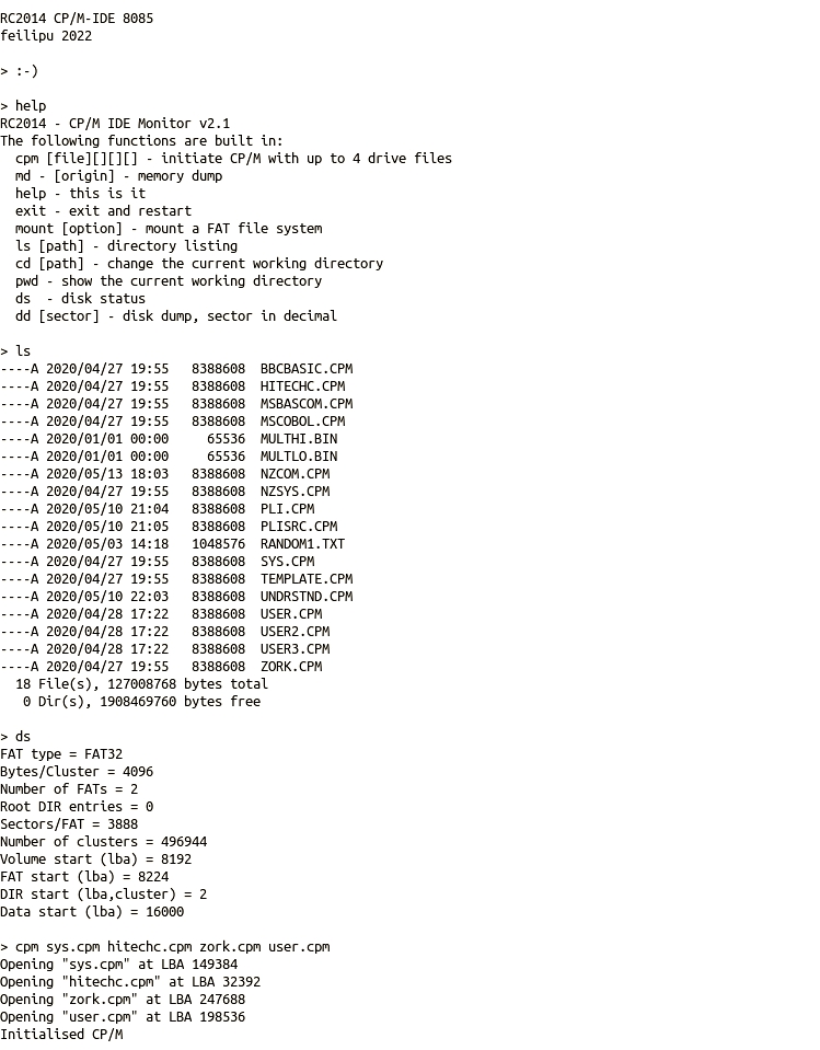
> fsed.cpm -f rc2014-8MB a.cpm
> cpmls -f rc2014-8MB a.cpm
> cpmcp -f rc2014-8MB a.cpm ~/Desktop/CPM/bbcbasic.com 0:BBCBASIC.COM

CP/M System Disk

Building a CP/M System disk is a personal choice. There are multiple utilities and applications available, and not all of them will be relevant to your own needs. However, to get started, the contents of the RunCPM system disk can be used. An extended version can be found here.

Also, the NGS Microshell can be very useful, so it has been added to the example system disk too. There is no need to replace the default DRI CCP with Microshell. In fact, replacing it permanently would remove the special EXIT function, added to the CP/M-IDE version of the DRI CCP, used to return to the shell.

CP/M Application Disks

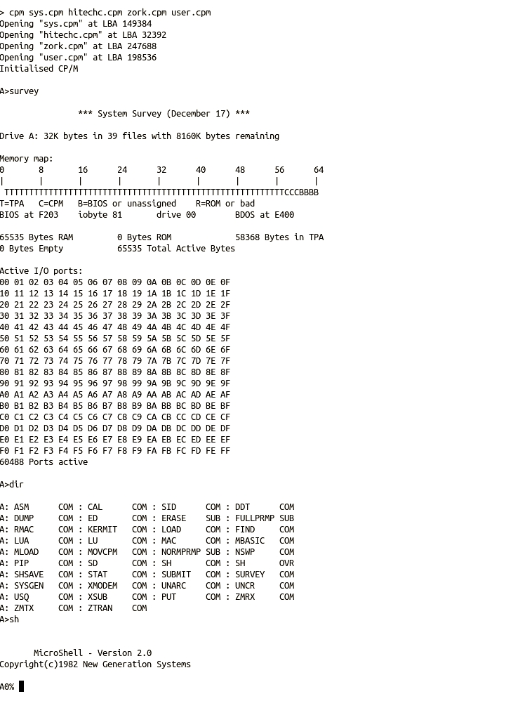
The CP/M Drives directory contains a number of CP/M disks containing commonly used applications, such as the Zork SeriesBBC BasicHi-Tech C v3.09, and MS BASIC Compiler v5.3. The MS Basic (Interpreter) v5.29 for 8085/Z80 is available in the system drive.

Of these applications above, the Hi-Tech C v3.09 suite continues to be updated and maintained by Tony Nicholson. Therefore it is useful to update the HITECHC.CPM.zip CP/M disk with the current release files.

Common Usage

When commencing a new project it can be convenient to start with a new clean working drive. Either the yash shell can be used from within CP/M to create a new drive file. The yash shell will properly extend the created file to ensure that it is contiguous on creation. Or the system drive can be temporarily attached to a PC and normal file management can be used to copy the template drive file provided, and rename the newly created drive file appropriately for the project.

Alternatively when working with a CP/M compiler, or editor, making a copy of the compiler drive file and working from that copy (rather than the original) can be quite useful.

On first boot into CP/M, mount the sys.cpm system drive and the new working drive. It can then be useful to copy some CP/M commands onto the working drive using PIP.COM, then the sys.cpm system drive does not need to be mounted on further boots. Generally XMODEM.COM is all that is necessary, as the CP/M CCP has DIR, REN, ERA, TYPE, and EXIT commands built in.

Then, on each subsequent boot-up of CP/M only the working drive in drive A: is necessary. After compiling a new project with z88dk, the work-in-progress application .COM or .bin can be uploaded to the RC2014 using XMODEM.COM and then tested. If the work-in-progress crashes CP/M or needs further work, then repeat the process as needed without danger of trashing files in any other drives.

Of course other development workflows are possible, as is simply mounting the ZORK games drive and playing an adventure game or two.

Building CP/M Software from Source

CP/M-IDE is quite unusual in that it is built with a unix like shell as the system loader. From the shell the CP/M system is started, but it is also possible to use the shell to read the FAT file system and provide directory listings, to print memory and disk sector contents, and to provide status for the attached drive. Other versions of CP/M for Z180 have file system write capability included, but due to the limited capacity (32kB) of the RC2014 ROM these additional file management functions had to be omitted from the CP/M-IDE ROM, though they are available from the yash shell application.

z88dk

The chicken or the egg? In this case the z88dk is both the starting point CP/M-IDE and the finishing point for developing CP/M-IDE applications.

There is an installation guide for z88dk, as well as a how to for the RC2014 with z88dk. Both of these can be followed to get your z88dk installation working and ready to build the CP/M-IDE.

By default the z88dk ACIA drivers are set up to use a 15 Byte transmit buffer. This needs to be changed to a 31 Byte transmit buffer, by changing this configuration to 0x20.

Also, if you wish to enable the shadow RAM setting where the Memory Module or SC108 Module is used then this setting needs to be changed to 0x01. This will enable the RAM copy stub and shadow RAM write and read functions. This is not relevant for the 8085 CPU build (which doesn’t support relocatable jump instructions), and is disabled by default for the Z80 builds (to support the 64k RAM Module).

And finally, the ide driver is selected by using either CF IDE (8-bit) or PPIDE (16-bit) interfaces. To use the PPIDE interface the CF Module configuration needs to be set to 0x00.

With these settings adjusted to suit the targeted hardware, the RC2014 libraries need to be rebuilt. Before rebuilding, be sure of whether shadow RAM should be enabled, and which IDE interface type should be enabled. he sure way to do this is by a full rebuild of z88dk, as both 8085 and Z80 libraries will be touched. it is done with the ./build.sh -c command from the root directory of z88dk. There are other alternatives, such as deleting the libraries that will have to be changed and executing the ./build.sh command.

z88dk-libraries

As well as two compilers, a macro assembler, and a large variety of useful tools, the z88dk is in essence a library of Z80 assembly language code covering all of the standard C requirements, and providing multiple options for implementing these libraries.

However, the z88dk doesn’t have C code libraries included. These are excluded because they can take too long to compile, and z88dk already takes quite a while to build as is. However the use of external libraries, and mainly C libraries is supported through the use of the z88dk-lib tool, which can import a compiled library and allow the linker to find it when a final binary application is being prepared.

For CP/M-IDE we need to have a high quality, reliable, fully functional FAT file system implementation. The most commonly used implementation is the ChaN FatFS. This code has been modified to work effectively with the Z80, and is provided in my z88dk-libraries.

For CP/M-IDE I have elected to use the SDCC compiler with the IY version of the libraries. For the CP/M-IDE 8085 the only option is to use the SCCZ80 compiler as it supports 8085 (and 8080) compilation.

As noted above, there is insufficient ROM available in the 32kB to support the full set of FAT file system functions, so we have to build a special version that is “read only”. There is a configuration that should be set to 1 to enable RC2014 read only in the file here. Then the library can be rebuilt with the following command lines.


> zcc +rc2014 -clib=new -m8085 -x -O2 --opt-code-speed=all -D__DISABLE_BUILTIN --math32 @ff.lst -o ../ff_85_ro
> zcc +rc2014 -clib=sdcc_iy -x -SO3 --opt-code-speed --max-allocs-per-node400000 @ff.lst -o ../ff_ro

This will produce two libraries. These library files need to be copied into the z88dk third party library directories manually. The z88dk-lib program will position the normal libraries correctly, and these special read only libraries can be simply placed beside the normal libraries in the z88dk file structure. To copy the normal libraries the command is here.

> z88dk-lib +rc2014 ff

The FAT file system libraries are now available for z88dk so we can move on to compiling CP/M-IDE

Building CP/M-IDE

The source code available in the RC2014 Github repository for CP/M-IDE is kept up to date. There are five versions, each tuned to suit their respective hardware characteristics. There is no “auto identification” of additional hardware. This implementation of the CP/M operating system supports only IDE attached FAT formatted disks and 1 or 2 serial ports, so that is all that is necessary. Any optional additional hardware available is supported by drivers built into the relevant application.

From the source directory of each version the command line identified here can be issued. The resulting .ihx file (renamed as .hex) can be compared with the provided HEX file. For interest it is worth compiling with the --list option, and studying the resultant assembly listings. This gives a good overview of the quality of code produced by the two compilers, and also the amount of space required to assemble the CP/M CCP/BDOS and BIOS components.

> zcc +rc2014 -subtype=acia85 -O2 --opt-code-speed=all -m -D__CLASSIC -DAMALLOC -l_DEVELOPMENT/lib/sccz80/lib/rc2014/ff_85_ro @cpm22.lst -o ../rc2014-8085-cpm22 -create-app
> zcc +rc2014 -subtype=acia -SO3 --opt-code-speed -m -llib/rc2014/ff_ro --max-allocs-per-node400000 @cpm22.lst -o ../rc2014-mini-cpm22 -create-app
> zcc +rc2014 -subtype=sio -SO3 --opt-code-speed -m -llib/rc2014/ff_ro --max-allocs-per-node400000 @cpm22.lst -o ../rc2014-sio-cpm22 -create-app
> zcc +rc2014 -subtype=sio -SO3 --opt-code-speed -m -llib/rc2014/ff_ro --max-allocs-per-node400000 @cpm22.lst -o ../rc2014-pro-cpm22 -create-app

Now we have a functioning CP/M-IDE Intel HEX file, which can be written to EEPROM and tested.

CP/M-IDE Applications

New applications can be built using either the zcc +rc2014 -subtype=cpm or zcc +cpm for Z80 targets, or for the CP/M-IDE 8085 use zcc +cpm -clib=8085 to build applications. There are example applications to test with in the z88dk examples directory including, for example, players for 8-bit sound.

Of particular interest is the yash shell, which runs on CP/M and allows full access to the underlying FAT File System. It provides all of the standard file management tools which are missing (due to space constraints) from the CP/M-IDE ROM shell. This can be found in the z88dk-ext/os-related/CPM directory, together with the instructions to compile it. It is also provided in the CP/M-IDE “system disk”.

How does it work?

This is a description of CP/M-IDE 8085 specifically. The versions for the Z80 are quite similar, and so this can also be used as a reference for their operation. However as the RC2014 8085 support is unique in z88dk it is worth noting the specifics here.

The CP/M-IDE 8085 build is based on the rc2014 target and acia85 subtype within z88dk. The 8085 CPU starts execution at address 0x0000 from /RESET, therefore the target must write an effective Page 0 including a jump to the start of code, and interrupt and trap vectors, before the main() program for the CP/M-IDE shell can be started. z88dk uses the m4 macro preprocessor tool to expand included assembly code, and the configuration files for the acia85 subtype are found in config_8085.m4.

The overall initialisation process for the acia85 subtype is found in CRT 2 startup code for the RC2014. Each target in z88dk has multiple subtypes, and each of these subtypes has its own CRT startup code specification. These startup specifications are fully expanded and can be read most efficiently by using the --list option when compiling the system.

Before diving into the startup process it is worth considering how and where drivers for the rc2014 acia85 build are obtained. As the acia85 subtype is hybrid across newlib and classic libraries within z88dk it is worth noting that most of the drivers for acia85 are obtained from the device and driver directories within the rc2014 target. However, stdio drivers for acia85 and basic85 subtypes are found in the classic library in the rc2014/stdio directory.

Further, using the characteristics of linker preferences, if we chose to override the library drivers with our own versions found within the CP/M-IDE BIOS then the library versions will be ignored. And that is the case, where we provide the ACIA, 82C55, and IDE drivers. This also means that before the main() function is started we need to copy these drivers to their correct location in RAM. This process is done by placing code in the code_crt_init section, as this code will be loaded and run prior to main() according to the memory model allocation.

Now we have our interrupt vectors completed, and the interrupt code placed with buffers initialised and ready to go. Our diskio and IDE drivers have been placed and now we can start our main shell user interface. Now we are parsing the command line using a shell system inspired by the example code by Stephen Brennan. Each of the commands implemented are self explanatory, and are mainly invoking one of the ChaN FAT file system functions. However the cpm command requires further description as this is the transition point from z88dk into DRI CP/M.

CP/M-IDE 8085 – Shell User Interface

The cpm function is called with up to 4 arbitrary file names, representing the 4 CP/M disks. These file names are tested and, if all the files provided are found to exist, the base LBA of each file will be written to a specific location in cpm_dsk0_base[], and processing will be handed over to the cpm_boot() function.

CP/M-IDE 8085 – CP/M User Interface

The _cpm_boot function is the CP/M cold boot mechanism. The CP/M cold boot will firstly toggle-out the lower 32kB of ROM to reveal a “clean” 32kB of RAM. At this point the 8085 interrupt and trap vector addresses must be written into Page 0 RAM, together with other important CP/M locations such as the I/O byte. Then control is passed to the rboot function to continue with the cold boot.

In the cboot process we should remember that the contents of the CCP/BDOS and the BIOS RAM have already been written to upper 32kB of RAM by the preamble code, so this process does not need to be repeated. This is different in the warm boot wboot process where we have to assume that the CP/M application or transient program will have overwritten the CCP and possibly also the BDOS, so we have to repeat the initialisation found in the preamble called by pboot.

As part of the cboot and wboot process, we check which CP/M disk is going to be used for our A: drive, by reading the LBA base, and then launching CP/M CCP shell by returning to the to the preamble code and falling through to _main.

From here it is all standard CP/M, and the contents of the CP/M Users Manual apply.

8085 Software

This covers creation of software support for the 8085 CPU within the framework of the z88dk and also with MS BASIC 4.7. Specifically, the 8085 undocumented instructions will be covered, and some usage possibilities provided.

8085 Microsoft BASIC 4.7

The Microsoft BASIC 4.7 source code is available from the NASCOM machine. Although the NASCOM machine was a Z80 machine there were only minor changes to the original Microsoft BASIC 8080 code. Therefore it is an ideal source to use to build a 8085 based system.

At this repository the 8085 RC2014 Microsoft BASIC is being developed. Currently fully working with the RC2014 ACIA Serial Module (from the RC2014 Classic ][). Some initial performance testing has been done, and there is little difference (< 1%) vs. the Z80 at the same frequency.

A version of Microsoft BASIC 4.7 for the 8085 CPU Module together with the Am9511A APU Module has been built, as well. This version adds the full performance of a hardware APU to the 8085 CPU providing the “complete performance package” for Microsoft BASIC.

Z88DK Support

Support for the 8085 processor is available from the z88dk. The sccz80 C Compiler, combined with the classic library and z88dk-z80asm assembler provide the necessary components.

Support for the 8085 CPU Module for the RC2014 has been provided using the underlying MS Basic as a program loader and debugging tool. This is reached through the rc2014 target basic85 subtype. This uses the standard RST serial interfaces (provided by MS Basic) and the HLOAD keyword to upload code compiled for $9000 origin (by default). Compiled programs can use any memory from $8400 through to $FFFF.

Also a rc2014 target ROM subtype acia85 has been provided to allow on-the-metal embedded applications to be written. The full 32kB of ROM and 32kB RAM is then available, with the option to toggle out the ROM if needed for CP/M or similar systems.

Within z88dk the mbf32 floating point math package has been optimised to support 8085 undocumented instructions.

The z88dk sccz80 C compiler is used for 8080, 8085 and Gameboy Z80 CPUs. This compiler is supported by the z88dk classic library. Over a few weeks, I reworked all of the sccz80 compiler support primitives (called l_ functions) to make them reentrant, and to optimise them for the respective CPU.

I’ve also reworked all of the z88dk string functions to support callee for the 8085 CPU. The callee calling mechanism is substantially faster than the standard calling convention. Also I’ve changed the loop mechanism for 8080 / 8085 / GBZ80 to use a faster mechanism. This consumes 5 bytes more for each function used, but reduces the loop overhead from 24 cycles per iteration to 14 cycles per iteration. Quite a substantial saving for extensively used functions like memcpy() and memset(), for example.

8085 Undocumented Instructions

Over the years since launch several very useful undocumented instructions designed into the 8085 have been found. These instructions are particularly useful for building stack relative code, such as required for high level languages or reentrant functions. However, perhaps because of corporate politics, these useful instructions were never announced, and thus were never widely implemented.

There is a reference to these instructions and their use in Intel mnemonics, but I prefer to use Zilog mnemonics. So I’ve modified the CLR table to support the 8085.

The z88dk-z80asm assembler provides synthetic instructions to simplify code for the different variants (it has also recently become a macro assembler) to simplify programming. These instructions are usually a useful sequence of normal instructions that can be issued with no side effects (eg. setting flags) that may streamline combined 8085 / z80 programming.

Discussion on the Instructions

Some things to think about (and then do).

  • Use the Underflow Indicator (K or UI) flag with 16 bit decrement and JP KJP NK instructions to manage loops, like LDIR emulation, more cleanly. 16 bit decrement overflow flag K is set on -1, not on 0, so pre-decrement loop counter.
  • Use the LD DE,SP+n instruction with LD HL,(DE) to grab from and LD (DE),HL to store parameters on the stack. Can use this with a math library to make it reentrant, for example, and also relieves pressure on the small number of registers.
  • Use the LD DE,SP+n instruction with LD SP,HL to quickly set up the stack frame. For example LD HL,SP+n, DEC H, LD SP,HL to establish 256-n stack frame.
  • Use RL DE together with EX DE,HL to rotate 32 bit fields.
  • Use RL DE together with ADD HL,HL to shift 32 bit fields.
  • Use RL DE as ADD DE,DE to offset into tables and structures.
  • Use SUB HL,BC for 16 bit subtraction.
  • Remember EX (SP),HL provides another “16-bit register”, if SP+2 is the location of the return, and SP+4 is the location of first variable.
  • Learn how signed arithmetic can be improved using the K flag.

Since we know that the 8085 undocumented opcodes are available in every 8085 device they can be relied upon for any 8085 system. The challenge will be to take existing 8080 programs, such as Microsoft Basic and CP/M, and implement improvements using these 8085 specific instructions.

In reworking the z88dk sccz80 l_ primitives to make them reentrant and to optimise them for the 8085 CPU, I have found the LD DE,SP+n instruction very important. Using this instruction it is possible to use the stack as effectively as static variable storage locations. The alternative available on the 8080 (and Z80) LD HL,N , ADD HL,SP takes 21 cycles, and clears the Carry flag. With the few registers available on the 8080 losing the Carry flag to provide state causes further cycle expense, spared with the 8085 alternative.

To load a single stack byte using LD DE,SP+n , LD A,(DE) is only 4 cycles slower than loading a static byte using LD A,(**). Also, loading a stack word using LD DE,SP+n , LD HL,(DE) is only 4 cycles slower than loading a static word using LD HL,(**). Given that variables can be used in-situ from the stack or pushed onto the stack from registers rather than requiring the overhead of the value being previously loaded into the static location, this small overhead translates into about 3 stack accesses for free compared to static variables.

One small design oversight in the Program Status Word of the 8085 is however quite annoying. The flags register contains a single bit that always reads as 0. A $FFFF pushed to AF is read back as $FF7F. This means that unlike in the Z80, it is not possible to use a POP AF , PUSH AF pair as a temporary stack store, which invalidates AF as one of the only 3 additional 16-bit registers as an option, making things even tighter when juggling the stack. I’d call it annoying AF.

The RL DE and SUB HL,BC instructions are very useful to build 16-bit multiply and divide routines effectively. They have contributed to useful optimisations of these primitives. The saving in bytes over equivalent 8080 implementations has allowed for partial loop unrolling, which also speeds up the routines by reducing loop overhead. Initially, I was concerned that the SUB HL,BC function didn’t include the Carry flag. But in hindsight it is not possible to effectively carry into the registers, and using the 8 bit SUB A,C , SBC A,B instructions via the A register is the way to manage long arithmetic.

Recently the LD DE,SP+n and LD HL,(DE) or LD A,(DE) instructions were used to replace the sccz80 z80 stack access routine LD HL,n, and ADD HL,SP followed by CALL l_gint or CALL l_gchar. Also the stack store routine CALL l_pint was replaced by LD (DE),HL. These small changes to the optimisation process have substantially improved the 8085 benchmarks, in both code size and performance, and they are now often better than similar z80 benchmarks.

CP/M-IDE 8085

The next challenge was to build a CP/M-IDE version for the 8085 CPU. The ingredients are ACIA serial drivers adapted for 8085, IDE and diskio drivers for 8085, and the ChaN FatFs library compiled for 8085, plus a 8085 adapted BIOS.

Modules required for CP/M-IDE 8085

When looking at the IDE drivers written previously for Z80 it was obvious that I’d gone out of my way to use Z80 instructions, which were actually slower than using 8080 instructions. So, I took the opportunity to rewrite an integrated solution for both Z80 and 8080/8085, for future maintenance.

The new CP/M-IDE 8085 code is very similar to the existing ACIA and SIO serial Z80 code, by design. I’ve tried to minimise the differences where ever possible. The remaining differences are mainly in the BIOS code, and relate to initialisation of the 8085 interrupts and the different CRT code used between Z80 and 8085 systems.

CP/M-IDE Modules installed in RC2014 Backplane 8

Am9511A (Intel 8231) APU Support

I’ve just added the Am9511 (Intel 8231) APU math library for the 8085 CP/M and other 8085 targets within z88dk. So now the 8085+Am9511 support is pretty much rounded out and complete.

To use the APU math library with CP/M, the library just needs to be linked with --math-am9511_8085.
For example:
zcc +cpm -clib=8085 -v -O2 n-body.c -o nbody --math-am9511_8085 -lndos -create-app

Just working through some maths benchmarks on my CP/M-IDE System now.

The Whetstone Benchmark for RC2014 results (7.3728MHz, hand timed) are:

  • 8085+MBF32 -> 78.2 Seconds -> 12.8 kWhetstone.
  • 8085+AM9511 -> 30.4 Seconds. -> 32.9 kWhetstone.

And for the n-body Benchmark the RC2014 results (7.3728MHz, hand timed) are:

  • 8085+MBF32 -> 252.3 Seconds.
  • 8085+AM9511 -> 69.3 Seconds.

So the the 8085+APU system is 2.5x to 3.6x faster than the best 8085 software maths library.
And what is very interesting is that these numbers also align very closely with the Z80+APU results.

Three Rings for the Z80

Over the past few years I’ve implemented a number of interfaces for Z80 peripherals based on the principal of the interrupt driven ring buffer. Each implementation of a ring exhibits its own peculiarities, based on the specific hardware. But essentially I have but one ring to bring them all and in the darkness bind them.

This is some background on how these interfaces work, why they’re probably fairly optimal at what they do, and things to consider if extending these to other platforms and devices.

The ring buffer is a mechanism which allows a producer and a consumer of information to do so with a timing to suit their needs, and to do it without coordinating their timing.

The Wikipedia defines a circular buffer, or ring buffer,  as a data structure that uses a single fixed-size buffer as if it were connected end-to-end. The most useful property of the ring buffer is that it does not need to have its elements relocated as they are added or consumed. It is best suited to be a FIFO buffer.

Background

Over the past few years, I’ve used the ring buffer mechanism written by Dean Camera in many AVR projects. These include interrupt driven USART interfaces, a digital audio delay loop, and a packet assembly and play-out buffer for a digital walkie-talkie.

More recently, I’ve been working with Z80 platforms and I’ve taken that experience into building interrupt driven ring buffer mechanisms for peripherals on the Z80 bus. These include three rings for three different USART implementations, and a fourth ring for an Am9511A APU.

But firstly, how does the ring buffer work? For the details, the Wikipedia entry on circular buffers is the best bet. But quickly, the information (usually a byte, but not necessarily) is pushed into the buffer by the producer, and it is removed by the consumer.

The producer maintains a pointer to where it is inserting the data. The consumer maintains a pointer to where it is removing the data. Both producer and consumer have access to a count of how many items there are in the buffer and, critically, the act of counting entries present in the buffer and adding or removing data must be synchronised or atomic.

8 Bit Optimisation

The AVR example code is written in C and is not optimised for the Z80 platform. By using some platform specific design decisions it is possible to substantially optimise the operation of a general ring buffer, which is important as the Z80 is fairly slow.

The first optimisation is to assume that the buffer is exactly one page or 256 bytes. The advantage we have there is that addressing in Z80 is 16 bits and if we’re only using the lowest 8 bits of addressing to address 256 bytes, then we simply need to align the buffer onto a single 256 byte page and then increment through the lowest byte of the buffer address to manage the pointer access.

If 256 bytes is too many to allocate to the buffer, then if we use a power of 2 buffer size, and then align the buffer within the memory so that it falls on the boundary of the buffer size, the calculation for the pointers becomes simple masking (rather than a decision and jump). Simple masking ensures that no jumps are taken, which means that the code flow or delay is constant no matter which place in the buffer is been written or read.

Note that although the number of bytes allocated to the buffer is 256, the buffer cannot be filled completely. A completely full 256 byte buffer cannot be discriminated from a zero fullness buffer. This does not apply where the buffer is smaller than the full page.

With these two optimisations in place, we can now look at three implementations of USART interfaces for the Z80 platform. These are the MC6580 ACIA , the Zilog SIO/2, and the Z180 ASCI interface. There is also the Am9511A interface, which is a little special as it has multiple independent ring buffers, and has multi-byte insertion.

Implementations

To start the discussion, let us look at the ACIA implementation for the RC2014 CP/M-IDE bios. I have chosen this file because all of the functions are contained in one file, which provides an easier overview. The functions are identical to those found in the z88dk RC2014 ACIA device directory.

Using the ALIGN key word of the z88dk, the ring buffer itself is placed on a page boundary, in the case of the receive buffer of 256 bytes, and on the buffer size boundary, in the case of the transmit buffer of 2^n bytes.

Note that although where the buffer is smaller than a full page all of the bytes in the buffer could be used, because the buffer counter won’t overflow, but I haven’t made that additional optimisation in my code. So no matter how many bytes are allocated to a buffer, one byte always remains unused.

Once the buffer is located, the process of producing and consuming data is left to either put or get functions which write to, or read from the buffer as and when they choose to. There is no compulsion for the main program flow to write or read at a particular time, and therefore the flow of code is never delayed. This is optimum from the point of view of minimising delay and maximising compute time. Additional functions such as flushpeek, and poll are also provided to simplify program flow, and init to set up the peripheral and initialise the buffers on first use.

With the buffer available then the interrupt function can do its work. Once an interrupt from the peripheral is signalled, the interrupt code checks to see whether a byte has been received. If not then the interrupt (in the case of the ACIA and ASCI) must have been triggered by the transmit hardware becoming available.

If in fact a byte has been received by the peripheral then the interrupt code recovers the byte, and checks there is room in the buffer to store it. If not, then the byte is simply abandoned. If there is space, then the byte is stored, and the buffer count is incremented. It is critical that these two items happen atomically, which in the case of an interrupt is the natural situation.

If the transmission hardware has signalled that it is free, then the buffer is checked for an available byte to transmit. If none is found then the transmit interrupt is disabled. Otherwise the byte is retrieved from the buffer and written to the transmit hardware while the buffer count is decremented.

If the transmit buffer count reaches zero when the current byte is transmitted, then the interrupt must disable further transmit interrupts to prevent the interrupt being called unnecessarily (i.e. with the buffer fullness being empty).

Multi-byte Receive

Both the SIO and ASCI have multi-byte hardware FIFO buffers available. This is to prevent over-run of the hardware should the CPU be unable to service the receive interrupt in sufficient time. This could happen if the CPU is left with its general interrupt disabled for some time.

In this situation, the SIO receive interrupt and the ASCI interrupt have the capability to check for additional bytes before continuing.

Transmit cut-through

One additional feature worth discussing is the presence of a transmit cut-through, which minimises delay when writing the “first byte”. Because the Z80 processor is relatively slow compared to a serial interface, it is common for the transmit interface to be idle when the first byte of a sequence of bytes is written. In this situation writing the byte into the transmit buffer, and then signalling a pseudo interrupt (by calling the interrupt routine) would be very costly. In the case of the first byte it is much more effective simply to cut-through and write directly to the hardware.

Atomicity

For the ring buffer to function effectively, the atomicity of specific operations must be guaranteed. During an interrupt in Z80 further interrupts are typically not permitted, so within the interrupt we have a degree of atomicity. The only exception to this rule is the Z80 Non Maskable Interrupt (NMI), but since this interrupt is not compatible with CP/M it has never been used widely and is therefore not a real issue.

For the buffer get function the only concern is that the retrieval of a byte is atomically linked to the number of bytes in the buffer.

For the put function it is similar, however as the transmit interrupt needs to be enabled by the put function atomcity is required to ensure that this process is not interrupted.

Interrupt Mode

Across the three implementations there are three different Z80 interrupt modes in play. The Motorola ACIA is not a Zilog Z80 peripheral, so it can only signal a normal interrupt, and can therefore (without some dirty tricks) only work in Interrupt Mode 1. For the RC2014 implementation it is attached to INT or RST38 and therefore when an interrupt is triggered it is up to the interrupt routine to determine why an interrupt has been raised. This leads to a fairly long and slow interrupt code.

The Z180 ASCI has two ports and is attached to the Z180 internal interrupt structure, which works effectively similarly to the Z80 Interrupt Mode 2, although it is actually independent from the Z80 interrupt mode. Each Z180 internal interrupt is separately triggered, however it still cannot discern between a receive and a transmit event. So the interrupt handling is essentially similar to that of the ACIA.

The Zilog SIO/2 is capable of being attached to the Z80 in Interrupt Mode 2. This means that the SIO is capable of being configured to load the Z80 address lines during an interrupt with a specific vector for each interrupt cause. The interrupts for transmit empty, received byte, transmit error, and receive error are all signalled separately via an IM2 Interrupt Vector Table. This leads to concise and fast interrupts, specific to the cause at hand. The SIO/2 is the most efficient of all the interfaces described here.

Multi-byte buffers

For interest, the Am9511A interface uses two buffers, one for the one byte commands, and one for the two byte operand pointers. The command buffer is loaded with actions that the APU needs to perform, including some special (non hardware) commands to support loading and unloading operands from the APU FILO.

A second Am9511A interface also uses two buffers, one for one byte commands, and one for either two or four byte operands. This mechanism in not as nice as storing pointers as in the above driver, but is required for situations where the Z180 is operating with paged memory.

I’ve revised this above solution again and do it with three byte operand (far) pointers, as that makes for a much simplified user experience. The operands don’t have to be unloaded by the user. They simply appear auto-magically…

Yet Another Z180 (YAZ180 v2)

Testing on the YAZ180 v1 , shown below, is now complete. I don’t want to use it for further driver and platform development, because the PLCC socket for the 256kB Flash is becoming worn-out.

It will continue to operate as an augmented Nascom Basic machine, with an integrated Intel HEX loader (HexLoadr) supporting direct loaded assembler or C applications.

img_0626

YAZ180 v1 at full configuration.

The new PCB for the YAZ180 v2 has been ordered.

These are some screenshots of the new PCB.


Update

Pi Day, March 14 2017.

After dwelling on the fact that the V2 PCB was really just a clean up the V1 PCB, with no additional features, I decided not to build the beautiful new PCBs that arrived today.

But rather, to create a new PCB with additional features.


New Features

When I originally designed the YAZ180 the breakout for the 82C55 was simply an interim design, to enable me to test the board. I was thinking of making an Arduino style pin-out, or something along those lines. But this is something much better.

Recently, after reading Paul’s page on interfacing an IDE drive to an 8051 microprocessor with the 82C55, I decided that adding IDE to the YAZ180 was a must-have feature.

So there is a new connector on the YAZ180 to break out the 82C55 pins, in IDE 44-pin 2mm format. I have not followed the design provided by Paul exactly. I’d note that his design and the earlier design by Peter Fraasse were specialist designs, which don’t support the generalised usage of the 82C55 chip, beyond the IDE functionality.

By the above statement I mean that in Mode 1 and Mode 2 for Port A and Port B, the PC2, PC4, and PC6 pins of the 82C55 device are designated registered strobe input pins /STB in input mode, or peripheral acknowledge /ACK in output mode. If an inverting output buffer is connected on these lines, then the registered input and output mode capability is lost. This would restrict the functionality of the 82C55 to simply Mode 0, being the mode that is used to create the IDE functionality.

As I’ve connected the three IDE address selection pins to PC2, PC4, and PC6, and these pins are not passed through an inverting buffer in the design, it is possible to use the 82C55 in any of its modes, and therefore to use the IDE 2.5″ 44-pin form factor to connect the YAZ180 82C55 ports to extension PCBs of any type or design.

As a connected IDE drive or other extension board may need to interrupt the CPU, I have connected the IDE INTRQ pin to the remaining inverting buffer to provide an input to the CPU on /INT0. As the /INT0 (or actually the INTRQ) input terminates on the IDE header, either a IDE drive through INTRQ, or either of the two 82C55 INTR pins, PC3 or PC0, can originate the interrupt.

I have reconfigured the Am9511A-1 to use the /NMI interrupt, as previously the /INT0 was configured.

The new YAZ180 v2 PCB has been ordered. YAZ180_v2_Schematic.

Happy Pi Day.

Update – RetroChallenge Day 1

I’ve decided to enter the RetroChallenge 2017/04 and my challenge is to read and write to an IDE drive using the newly configured IDE interface on the YAZ180v2. But before I can write the code for the IDE interface, there’s a bit of building and testing that needs to be done.

The new PCBs arrived a few days ago, and they look great. But Arduino Day and the first day of the RetroChallenge 2017/04, 1st April, seemed like a good day to lay them out.

P1080754

New PCBs. 2oz Copper, 2mm thick. Opulent.

I was hoping to lay build several boards at once, but somehow I forgot that there was only one RAM and one FT245 device in my component stocks. That means that I had to satisfy myself with just one board for now.

Note the suitably Retro PowerMac (circa 2001) driving the layout guide screen.

P1080755

Adhoc Workspace

This is the board just before cooking. Respect to anyone who notices the substantial noob layout mistake. Anyway, after a small smokey explosion, everything was rectified.

P1080758

Two YAZ180 versions, side by side.

This is the finished build of the YAZ180 v2. Looks very tasty. Retro goodness.

P1080761.JPG

Fully populated YAZ180 v2 PCB.

I’m still working on fixing an issue with my code, which I noticed when experimenting with the Am9511A APU, and inserting an Interrupt Jump Table. Basically, I’m getting jumps to odd or  random locations, which is detected buy filling unused locations with 0x76, the HALT, OpCode. The most common address where the HALT is executed at is 0x00C3.

Previously, I’d been filling unused locations with 0xFF, the RST 38H OpCode shared with the INT0 location 0x0038, which was causing the APU to be triggered inappropriately. This issue has me snookered. I can’t move on, in the software sense, until it is resolved .


This slideshow requires JavaScript.

Update – RetroChallenge Day 8

Well this week was one of the most frustrating weeks ever, in terms of time spent vs. results obtained.

There are two major projects in hand. 1. Getting the YAZ180 v2 running, and 2. resolving the software issue plaguing my initialisation code.

Hardware issues

Bringing up a new piece of hardware is never easy. Initially, nothing can be trusted to work, and everything needs to be checked against the design, and then even the design checked for correctness. Bringing up the YAZ180 v1 was very time consuming, because I had to develop the PLD design during the process, as well as checking that all the hardware was sorking as it should. I thought that bringing up the YAZ180 v2 would be easy. Just solder it together and win. But it has not been so simple.

Essentially, after a week of working on this every evening, I don’t know why it is not working correctly. All the standard things, volts, clock, stuck address and data lines, etc are all working correctly. But it still doesn’t work. And, it may not be just one thing that is wrong, but if anything is not perfect it just won’t work.

After a few days of testing, I found that I’d programmed the PLD devices with an old version of the CUPL code. Nearly right, but not exactly right. Once I’d isolated that issue, by ensuring the new GAL devices worked perfectly in the V1 board, I thought it would be enough. But no. There’s still something wrong.

My current thought is that somehow, either electro-static damage or heat damage, the RAM is unreliable. But, I’m not sure enough of this to unsolder the RAM device and replace it. I’ll be spending this weekend on resolving this problem.

Software issues

Because of the effort I’ve been putting into resolving the hardware issues, I’ve not been able to solve the software issue apparent in the YAZ180 initialisation and serial code. I’ve documented the issue on Github.

My lesson learned is NOT to fill unused memory with 0xFF bytes. This causes RST 38H jumps to the INT0 location when the PC is incorrectly loaded, and can be very distracting. Best to fill unused memory with either 0x76 HALT bytes, to see where things became broken, or with 0xC9 RET bytes to just float over the underlying issue.

I’ll need to fix this properly, but it has consumed several weeks of effort, and I’m not much closer to resolution.

Update – RetroChallenge Day 10

The weekend was unkind, but today some new eyes (literally) have brought successes.

Hardware Issues

After doing quite a bit of further testing, I’m fairly sure that I’ve damaged the RAM and will need to replace it. So, I’ve ordered a hot-air solder gun. Should have had one for a long time. Finally, I’ve got a round-‘tuit. I’ll have to order some replacement components too, which will result in being able to make additional boards as well.

Software Issues

Finally, I’ve resolved my issue. What we had here was a classic “failure to understand”. Somewhat embarrassed to leave this here for Internet eternity.

  • Z80 vectors are supported by a JUMP table.
  • Z180 vectors are supported by an ADDRESS table.

Insert JP instructions into an address table and you will have a very very bad day.

Or in my case, quite a few of them.

This issue cost so much time. But at least on the up side, I’ve written robust Z80 and Z180 vector tables, improved my ASCI code, and cleaned up initialisation code, in trying to track this down.

Also finally, I now understand. Which is the entire point, anyway.

Update – RetroChallenge Day 17

Following up on the success of last weekend, I was hoping to have a lot of achievement to write about today. Unfortunately, it has been a grind this week too.

I have been distracted back into the original project that unearthed my previous software problem, and led me along the path to getting a much better understanding of the Z180 CPU, and then solving the issue. The original project was building an interrupt driven driver for the Am9511A-1 Arithmetic Processing Unit.

I’ve spent pretty much the past week on this code, and digging through it with a fine tooth comb. I’m now of a belief that my Am9511A driver code is correct, but my hardware is not correct and may never be correct.

The issue lies with the requirement for the Am9511A to have the Address lines and Chip Select signal remain valid for 30ns following raising of the Write signal. Unfortunately, the Z180 only maintains valid address lines for 5ns following Write. This means that writing to the AM9511A APU is very much a hit and miss affair, with miss being the most likely outcome. I’m still thinking about ways to bodge this to work. But, I think that it may just be too hard to get the old APU to work with a modern CPU. More on this later.

This week I’ll be working on the PaulMon IDE code, and migrating it from 8051 to Z80 nomenclature, and trying to get it to compile.

Update – RetroChallenge Day 21

Well the last couple of days have been exciting, as I found a way to make the Am9511A APU work. A hint from a fellow competitor (on working with the MC6809 CPU) inspired me to look further for information on options to fix the hardware interface.

The Z180 E CLOCK

The Z180 has an almost undocumented feature, called the E Clock. Yes, it is documented in datasheet that it exists, but there’s no real background that I can find as to why it exists, except that is for a Secondary Bus Interface. This pin and signal doesn’t exist on the Z80, for example. Anyway, since it has the same name as a signal on the MC6809, I thought it might be worth looking at it. It turns out that the E Clock provides a shortened version of the WR and RD cycles. Which is exactly what we need.

One caveat however, when running at doubled PHI rates (i.e. 1:1 PHI – CLK) the shortening of the E Clock signal is not sufficient to drive the APU successfully. At 18.432MHz, the PHI/2 timing is 27ns. Therefore, the minimum of 30ns between release of WR and CS is not always held. This means that we’ll need to keep the PHI at half CLK whilst using writing data into the APU. In practice this means that using the APU requires we cut the CPU clock by 50% or PHI/2 being 57ns, to ensure the trailing 30ns is provided.

Anyway. Good news. With the revised timing, the Am9511A-1 is working.

Am9511A FDIV

Am9511A APU Floating Divide in 115us

The E Clock is not an inverted signal, so to generate the active low APU_WR signal we have to first invert it, then OR it with the WR signal. For the purposes of testing, I’ve got a little breadboard with a GAL on the side, but later I’ll build a new PCB and add in a SN74LVC1G97 little logic device to provide the APU_WR signal.

Am9511A FDIV PUPI

Am9511A APU FDIV PUPI command interval 128us

Am9511A FDIV PHI6 Cycles

Am9511A APU FDIV in 179 Phi/6 Clock cycles

So now we see the Am9511A APU FDIV floating point divide takes about 101us to 115us when running at 1.536MHz, or from the datasheet 154 to 184 clock cycles. In 101us, the Z180 CPU at 36.864MHz produces 3,723 cycles. To produce a floating point divide using the Lawrence Livermore Library requires about 13,080 cycles, according to the AM9511A Floating Point Processor Manual by Steven Cheng. Therefore, we are still substantially faster than antique software on a modern Z180!

Update – RetroChallenge Wrap Up

Well the month of RC2017/04 didn’t go quite as planned. My original intention was to have the YAZ180v2 working very quickly, then get straight down to porting Paul’s IDE code from 8051 to Z180 to get the new IDE interface working. But, there were several speed bumps along the way.

Gaining an education

Since I just started on this whole Z80 processor and assembly language programming thing a few months ago, I don’t have a long history of coding to fall back on. I had written some code for the Z80 in the RC2014 hardware, which I then tried to use on the Z180 in the YAZ180. But, there is a subtle difference in “generation” between the way the interrupt vectors work across the two machines. Obvious, once you know about it but a real “time killer” if you don’t.

Firstly, filling unused space in your assembly program with 0xFF is a very dangerous thing to do in Z80 assembler, particularly if you don’t understand that 0xFF is the op code for RST38, which is a single byte jump to the same location as the Interrupt 0 in IM1 mode. It would make more sense to fill the unused space with 0x76, which is the HALT instruction, to trap an unexpected program counter value.

Look before you leap

Secondly, the interrupt vectors on the Z80 were designed to contain code, and the PC is just loaded with the address of the vector, and execution begins from there. So for an INT0 (or RST38) execution begins from 0x0038. But, the interrupt vectors on the Z180 are designed to hold an address. The difference being that an interrupt will load the PC with the contents of the two bytes at the vector, and then begin execution from there. I think this difference is a sign of the generational difference between the two implementations. One of the clearest differences I can find, anyway.

Timing is everything

One of the goals for the YAZ180 is to bring some old chips back to life, in a modern platform. Along with the TIL311, GAL16v8, and 82C55 devices, the Am9511A holds pride of place as the very first arithmetic processing unit ever made. I’ve invested far too much time in getting the Am9511A to work, but it is important to me that my project can make it work.

I believed that I had devices that were specified to run at 3MHz but which in fact didn’t. That may be incorrect. More likely was that I wasn’t driving them properly, because my timing was out. I will need to go back and test them all again.

Here the issue is that the Am9511A requires extended validity of data and chip select signal, following the validity of the write signal. At least 30ns is required. This is not provided by the Z180 in its normal timing, although in the configuration I have it, coincidentally because I’d buffered the data bus, it is nearly right. Only the chip select line was being incorrectly handled.

I was nearly giving up but then a tweet from a fellow RC2017/04 competitor gave me the inspiration to look further. It turns out that the Z180 has a secondary I/O timing signal called the E Clock. This signal is not present on the Z80, and as I didn’t understand its purpose I’d left it unconnected in the YAZ180.

Whilst the Zilog datasheets on the Z180 completely gloss over the purpose of the E Clock signal, by simply not mentioning it, the original Hitachi 64180 datasheets do mention it. The original purpose of the E Clock signal was to provide timing for “a large selection of 6800 type peripheral devices” including the “Hitachi 6300 CMOS series (6221 PIA, 6350 ACIA, etc) as well as the 6500 family devices”.

In summary, the E Clock provides a signal that is half a T cycle shorter than the write signal. It means that gating the write signal with the E Clock would allow me to release the APU write signal sufficiently early to maintain the extended chip select timing required. Basically, the APU won’t operate with a Z180 T Cycle any less than 60ns, or 16.6MHz. So in my implementation, the PHI clock will need to run at half speed or 9.234MHz, whilst the Z180 is using the Am9511A. Unless I cook up another plan.

Zapped

And the final note from this month is that I believe my very poor ESD protocol has led to the destruction of the SRAM on my YAZ180v2. Therefore I had to desolder it (and it looked so nicely done) to remove it, and order some new components.

Ordering new components is always a bit of a hurdle for me. I’ve collected quite a few things that I don’t use, so I tend to ration myself on purchases vs. progress. Finally, at the end of the month I ordered more components to build further YAZ180 boards, and some spare SRAM to enable me to repair the one I have made already.

It continues to amaze me just how much difference there is in the cost to build an Arduino AVR board (basically just a chip at the most essential level), vs something like the YAZ180. The YAZ180v2 bill of materials, excluding specials like the GAL16V8D, TIL311, and Am9511A devices that I have to find of eBay, comes to over $150 Australian!!! We need to export more coal, to get the AUD dollar back up there!

And that’s it for my RC2017/04 month. Soon as the parts arrive I’ll be completing the YAZ180v2, and then testing the IDE interface. I hope that will be done before the end of 2017/05.

Update – Post RetroChallenge

Well good news. The only issue was a bad solder joint on the new SRAM chip. Now the YAZ180v2 is running, and I can get onto translating the IDE code from 8051 to Z80.

IMG_0698

YAZ180 with IDE drive attached.

I’ve sourced code from both PJRC in 8051 mnemonics for an 8255 PIO and from Retroleum in Z80 mnemonics for an 8 bit interface. Between the two of them, together with the examples from the OSDev Wiki, it should be easy to make a fairly robust implementation. And, on May 18th, the driver code was finally working.

Next activity is to integrate this into the z88dk, and then using the FAT-FS code from Elm ChaN, get the disks properly working.

Update – August 2017

Over the past few months progress has been made on various fronts with the YAZ180v2. Firstly, the IDE interface is fully working, and has been integrated into z88dk. Also, the issues with the Am9511A-1 APU have been resolved, and a working driver has been integrated into z88dk. While I still have to revise the C interface for these two pieces of code, because I’m still learning this, the development work is now done.

I am particuarly happy about getting the Am9511A APU working, as this was causing me the most technical difficulty, and stretched my understanding the most. I’m also happy that the capability in the Am9511A seems to be realised through performance improvements in arithmetic computation.

Over the coming months, I hope to resolve the remaining untested components in the YAZ180. These include the parallel programming interface, to allow the YAZ180 to be “cold loaded”, to protect against bricking the system, if a user doesn’t have a EEPROM or Flash writer. I’m still in two minds abou this feature, as the cost of the FT245 device and USB socket is about the same as a stand alone EEPROM writer, and the parallel programming interface consumes space that could be otherwise used for an SPI or USB interface, for example.

I also need to test the I2C interfaces, and debug the driver that I wrote back in May (still unused) to complete the feature set.

With this done, I’ve now done a new minor revision of the hardware, to clean up the issues that have been noted over the past months.

Open Issues

  • APU – Gate E clock with WR to produce shortened APU WR
  • NMI – remove this from the APU, and terminate high. Not CP/M compatible.
  • INTO – reconnect it to the APU.
  • 5V – Power inductor spacing.

Update – October 2017

Well, I fixed the issues and then convinced myself that there needed to be Yet Another feature added to the YAZ180, before I signed it off. So now, the v2.1 board has access to the Internet through an ESP-01S AT interface.


This slideshow requires JavaScript.

I sell on Tindie

Building up this new board will be November and December’s activity, together with building a complete YABIOS (Yet Another BIOS) to make use of all of the features packed into the YAZ180 board. I’ll be picking the best bits, IMHO, from the Cambridge Z88, ZX Spectrum, and CP/M 2.2 – ZSystem to build a banking capable YABIOS, supporting 1MByte of address space.

Update – August 2018

I seriously need to write another blog on the YAZ180. But I guess the Github commits just speak for themselves. There are only three things left on the to-do list. 1. finish the firmware loading program. 2. rewrite the I2C interface. And 3. implement FreeRTOS as a hypervisor allowing multiple 60kB applications to run simultaneously.

Here’s a picture of an application, which was one of the early drivers for building the YAZ180, a mass-storage platform for my HP48 calculator.

IMG_1572

YAZ180 communicating with HP48 using Kermit on ASCI1 (TTY).

Z80 C code development with Eclipse and z88dk

I’m building a Z180 based development board called the YAZ180 for the 40th anniversary of the Z80 processor. As part of that process, I need to have a development environment that supports the Z80 and the Z180 processors. As I haven’t finished building the YAZ180 yet, I’ll be testing the development environment on the RC2014 platform in the interim.

IMG_0084

RC2014 Serial I/O & CPU

There are a couple of major differences in the workflow required to program the YAZ180 from the RC2014. The RC2014 requires an EEPROM programmer to burn the resulting HEX file into its ROM. Eventually, the YAZ180 will use a PERL program to manipulate a parallel port to programme FLASH memory. However, for the purposes of setting up a development environment they are essentially the same.

img_0404

YAZ180 Prototype

To set up the required environment, we’ll need to have:

  • A C compiler suite capable of generating HEX or BIN files for burning onto the hardware.
  • Applicable .CRT files to initialise the CPU and RAM, either Z80 or Z180 specific, so that the C environment can be properly launch.
  • Suitable library files for USART, and other interfaces, appropriate for the hardware in use.
  • Configuration to allow the correct tools and libraries to be found from within the Eclipse IDE.

A C Compiler Suite

There are only a few options for C compilers for the Z80 processor. There is a the Zilog development environment, and the SASM Softools. On the open source side there are two options worth mentioning, being the Small Device C Compiler (SDCC) and the Z88DK Small C Compiler.

There are a few reviews on the Internet of the various options, but in summary the best outcome seems to be to use the Z88DK together with the SDCC Compiler, and the “new library”.

The Z88DK team contributed this information to the RC2014 forum, which gives an overview of the options.

There are two C compilers. One C compiler is sccz80 which is derived from small C but z88dk’s version has seen continuous development over the past 30 years so it’s had most of the limitations of small C removed. For example, floating point is supported, ANSI C declarations are supported, 8/16/32-bit integers are supported and so on. It is a little short of C89 compliance with a few notable non-compliances being multi-dimensional arrays and function pointer prototyping.

The other C compiler is a patch of sdcc, another open source compiler that attempts to implement subsets of C89, C99 and C11. sdcc is an optimizing compiler and z88dk’s patch improves on sdcc’s output by supplying some Z80 bugfixes not yet incorporated into sdcc itself and by supplying a very large set of peephole rules to further improve output.

You can choose which C compiler you use by selecting the appropriate switch on the command line. In your makefile you are using sccz80. To use sdcc, “-clib=sdcc_ix” or “-clib=sdcc_iy” would appear in the compile line.

And then there are two C libraries.

The classic C library is the C library that has always shipped with z88dk. It has many crts available for it that allows compiling for a lot of target machines out of the box. The level of library support varies by target with the best supported having sprite libraries, sound, graphics, etc supplementing the standard c library. It is mostly written in machine code and has a small stdio implementation. However, at this time it cannot be used to generate ROMable code as it mixes variables with code in the output binary. It’s also not compatible with sdcc at this time. Both of these issues are being addressed now.

The new C library is a rewrite from scratch with the intention of meeting a subset of C11 compliance. It is 100% machine code, is written to be compatible with any C compiler, and can generate ROMable code with separation of ROM and RAM data. The stdio model is object oriented and allows device drivers to be written using code inheritance from the library. Although it’s not finished (it’s missing disk io and non-blocking io), it is in an advanced state.

The choice of C library is made on the compile line. “-clib=new”, “-clib=sdcc_ix” and “-clib=sdcc_iy” all use the new C library. Anything else uses the classic C library. In order to generate ROMable code, you should really be using the new C library.

The sdcc_ix and sdcc_iy libraries are chosen when sdcc is the compiler and are selected between by either ”-clib=sdcc_ix” or ”-clib=sdcc_iy” on the compile line. The difference between the two is which index register the C library uses. “sdcc_ix” corresponds to the library using ix and “sdcc_iy” corresponds to the library using iy.

It’s always preferable to use the “sdcc_iy” version of the library because this gives sdcc sole use of ix for its frame pointer while the library uses iy. If “sdcc_ix” is selected, sdcc and the library must share ix which means the library must insert extra code to preserve the ix register when it is used. This means the “sdcc_iy” compile will be smaller.

z88dk’s C library is different from other compilers in that it is written in assembly language, so it is more compact and faster than other z80 C compilers.

Installation instructions for z88dk here and I’d recommend using a nightly build rather than the last release. z88dk is an active project and it changes quite quickly. If you run on windows or mac there are binary packages available from the nightly build. For linux or other targets there are instructions for building from source and for patching sdcc to create zsdcc, z88dk’s version of sdcc.

Just to add for the ROM target: the new C lib allows the stored data section to be lz77 compressed so this should save a few bytes in the stored binary in ROM. Another thing you could do is compile a program for RAM and store a compressed copy in ROM that gets decompressed into RAM at startup.

Z88DK & SDCC Installation

I’m installing Z88DK and SDCC onto Ubuntu 16.04 AMD64 and, since the machine has recently been refreshed, many packages that were required for the install were missing.

Clone the latest nightly checked Z88DK Github package:

git clone https://github.com/z88dk/z88dk.git

sudo apt-get install expect texinfo libxml2-dev flex bison gputils libboost-dev

This will create a populated z88dk directory in the current working directory.

To succeed in building the ‘z80svg’ graphics tool you need the ‘libxml2’ library to be previously installed, although its absence will not prevent the rest of the kit from building.

Then, just type:

cd z88dk
git submodule update --init --recursive
chmod 777 build.sh (just in case)
./build.sh

You can run z88dk keeping it in the current location, all you need to do is to set the following environment variables.

Supposing you have bash (most likely it is your system default shell) and you want to keep z88dk in your home directory, you can configure it permanently in this way:

vi ~/.profile

Modify the configuration by adding these lines (with the appropriate paths).

export PATH=${PATH}:${HOME}/z88dk/bin
export ZCCCFG=${HOME}/z88dk/lib/config

A system install is not supported in this release of Z88DK.

Then to install the SDCC compiled specifically for the Z80 and Z180 these are the instructions.

Check out the current development version of sdcc. If you already have the sdcc-code tree available from a previous checkout you can instead perform an update.

svn checkout svn://svn.code.sf.net/p/sdcc/code/trunk@14210 sdcc-code
# or if you're doing this to refresh your sdcc installation...
cd sdcc-code
svn update -r 14210

You will have to apply the svn patch found in sdcc_z88dk_patch.zip and build sdcc from source. Copy “sdcc-z88dk.patch” from inside sdcc_z88dk_patch.zip into the sdcc-code directory.

The supplied configuration options disables all ports other than the Z80 family ports, and turns off compilation of many libraries. This will prevent errors from completing the build process, and results in a smaller binary.

cd sdcc-code/sdcc
patch -p0 < ../sdcc-z88dk.patch
cd sdcc
./configure --disable-ds390-port --disable-ds400-port --disable-hc08-port --disable-s08-port --disable-mcs51-port --disable-pic-port --disable-pic14-port --disable-pic16-port --disable-tlcs90-port --disable-xa51-port --disable-stm8-port --disable-pdk13-port --disable-pdk14-port --disable-pdk15-port --disable-pdk16-port --disable-mos6502-port --disable-mos65c02-port --disable-r2k-port --disable-non-free --disable-device-lib --disable-ucsim --disable-packihx --disable-sdcpp --disable-sdcdb --disable-sdbinutil --prefix=`pwd`/sdcc-install
make all

Copy the patched and compiled sdcc executable from the src directory to {z88dk}/bin and rename it “z88dk-zsdcc”.

cp src/sdcc {z88dk}/bin/z88dk-zsdcc

Undo the patch.

cd ..
patch -Rp0 < ../sdcc-z88dk.patch

You can stop here and verify the install was successful below. Keeping the sdcc source tree in an unpatched state can allow you to update the zsdcc binary by repeating the steps above as sdcc itself is updated. Both z88dk and sdcc are active projects that see frequent updates.

To verify that sdcc is usable from z88dk, try compiling sudoku.c for the rc2014 target using sdcc:

zcc +rc2014 -subtype=rom -v -m -SO3 --max-allocs-per-node200000 --c-code-in-asm --list sudoku.c -o sudoku -create-app

Using the C compiler

Assuming we have a source code called test.c

#include

main()
{
return(0);
}

We can compile it and produce binary CODE and DATA sections. The CODE and DATA sections need to be concatenated, and then assembled into an Intel HEX file by appmake.

zcc +rc2014 -subtype=rom -v -m -SO3 --max-allocs-per-node200000 --c-code-in-asm --list test.c -o test -create-app

The binary code can be checked by installing and then using a disassembler z80dasm

sudo apt install z80dasm
z80dasm --address --labels --origin=0x0 test.bin

Loading the Code

Eventually the YAZ180 will have a hardware USB interface, and Perl based loading mechanism to load both RAM and Flash storage. But, since I broke the only extant hardware interface, getting this function working will have to wait.

In the interim, I have to load assembled machine code into the YAZ180 via a back door, being via the YAZ180 Nascom Basic which I also have running. The back door is opened because the Basic interpreter has the capability to 1. insert or POKE arbitrary bytes into RAM located at any address, and 2. via a Basic instruction USR(x) jump into any location in RAM and begin executing code.

Because of these POKE, PEEK, and USR(x) instructions we can load our own program in two different ways. Firstly, we can encode our program as a series of poke instructions, and then let the Basic interpreter load the program code byte by byte. Whilst this is a practical way of loading smaller programs, it is quite inefficient and also somewhat difficult to confirm that the program is loaded into RAM correctly. Also, this method cannot handle writing to Flash, as the POKE command is only designed for RAM.

The second method is to take a two step approach. Use the previous method of generating POKE instructions to insert a small Intel HEX format capable program, or HexLoadr, into the RAM, and then use the USR(x) instruction to launch the HexLoadr which also reads the serial port, and inserts the read HEX formatted bytes into RAM or Flash. The first advantage of this method is efficiency because the density of program bytes is substantially higher in Intel HEX than it is in POKE instructions. Also, because we can craft the HexLoadr with any functions we choose, we can also enable it to configure the Z180 MMU using the Intel HEX Extended Segment Address, and program the entire physical address space of the YAZ180, and we can deploy capability to write Flash memory making changes written then permanent.

HexLoadr

The goal of the HexLoadr program is to load your arbitrary program in Intel HEX format into an arbitrary location in the Z80 address space, and allow you to start the program from Nascom Basic.

There are are several stages to this process.

  • The HexLoadr.asm loader program must be compiled into a binary format, HEXLOADR.BIN.
  • HEXLOADR.BIN must then be converted to a series of POKE statements using the bin2bas.py python program.
  • These POKE statements are then loaded through the serial interface into Nascom Basic to get the HexLoadr program placed correctly into the RAM of the RC2014 or YAZ180 machine.
  • The starting adddress of the HexLoadr program must be inserted into the correct location for the USR(x) jump out of Nascom Basic.
  • Then the HexLoadr program will initiate and look for your program’s Intel HEX formatted information on the serial interface.
  • Once the final line of the HEX code is read, the HexLoadr will return to Nascom Basic.
  • The newly loaded program starting address must be loaded into the USR(x) jump location.
  • Start the new arbitrary program by entering USR(x).

Important Addresses

There are a number of important Z80 addresses or origins that need to be modified (managed) within the assembly and python programs.

Arbitrary Program Origin

Your program (the one that you’re doing all this for) needs to start in RAM located somewhere. Some recommendations can be given.

For the RC2014 with 32kB of RAM, and the YAZ180 with 56kB of RAM available, when Nascom Basic initiates it requests the “Memory Top?” figure. Setting this to 57343 (0xDFFF), or lower, will give you space from 0xE000 to 0xFFFF for your program and for the hexloader program.

The eXit option on my initiation routine for Nascom Basic is set to jump to 0xE000, Under the assumption that if you are jumping off at restart you are interested to have a large space for your arbitrary program.

For the YAZ180 with 56kB of RAM, the arbitrary program location is set to 0x2900, to allow this to be in the Common 0 Space for the MMU. Further for the YAZ180, the MMU Bank Space is configured from 0x4000 through to 0x7FFF so that the entire address space can be written by configuring the physical location at which the HexLoader operates.

HexLoadr supports the Extended Segment Address Record Type, and will store the MSB of the ESA in the Z180 BBR Register. The LSB of the ESA is silently abandoned. When HexLoadr terminates the BBR is returned to the original value.

HexLoadr Program Origin

For convenience, the HexLoadr program is configured to load itself from 0xFF00. This means your arbitrary program can use the space from 0xE000 to 0xFEFF without compromise. Further, if you want to use a separate stack or heap space (preserving Nascom Basic) the HexLoadr program space can be overwritten, by setting the stack pointer to 0x0000 (which decrements on use to 0xFFFF).

This can be changed if substantial code or new capabilities are added to the HexLoadr program

RST locations

For convenience, because we can’t easily change ROM code interrupt routines already present in the RC2014 or YAZ180, the serial Tx and Rx routines are reachable by calling RST instructions.

* Tx: RST 08H expects a byte in the a register.
* Rx: RST 10H returns a byte in the a register, and will loop until it has a byte to return.
* Rx Check: RST 18H will return the number of bytes in the Rx buffer (0 if buffer empty) in the a register.

Program Usage

  1. Select the preferred origin .ORG for your arbitrary program, and assemble a HEX file using your preferred assembler.
  2. Confirm your preferred origin of the HexLoadr program, and adjust it to match in the hexloadr.asm and bin2bas.py programs.
  3. Assemble hexloadr.asm using TASM to produce a HEXLOADR.BIN file using this command line.
    c:> tasm -80 -x3 -a7 -c -l -g3 d:hexloadr.asm d:hexloadr.bin
  4. Produce the “POKE” file called hexloadr.bas by using the python command.
    $ python bin2bas.py  HEXLOADR.BIN > hexloadr.bas
  5. Start your RC2014 or YAZ180 with the Memory top? set to 57343 (0xDFFF) or lower. This leaves space for your program and for the HexLoadr program.
  6. Using a serial terminal (assuming your machine is located at device /dev/ttyUSB0) either copy and paste all of the POKE commands into the RC2014, or upload them using a slow (or timed) serial loading program. If desired the python slowprint.py program can be used for this purpose.
    $ python slowprint.py /dev/ttyUSB0
  7. From the ok prompt in Basic, start the HexLoadr program with PRINT USR(x).
  8. Using a serial terminal, upload the HEX file for your arbitrary program that you prepared in Step 1. If desired the python slowprint.py program can also be used for this purpose.
    $ python slowprint.py /dev/ttyUSB0
  9. Using POKE commands relocate the address for the USR(x) command to point to .ORG of your arbitrary program.
  10. When HexLoadr has finished, and you are back at the Basic ok prompt start your arbitrary program using PRINT USR(x), or other variant if you have parameters to pass to your program.

Credits

HexLoadr is derived from the work of @fbergama and @foxweb.