 Over the past few years I’ve implemented a number of interfaces for Z80 peripherals based on the principal of the interrupt driven ring buffer. Each implementation of a ring exhibits its own peculiarities, based on the specific hardware. But essentially I have but one ring to bring them all and in the darkness bind them.
This is some background on how these interfaces work, why they’re probably fairly optimal at what they do, and things to consider if extending these to other platforms and devices.
The ring buffer is a mechanism which allows a producer and a consumer of information to do so with a timing to suit their needs, and to do it without coordinating their timing.
The Wikipedia defines a circular buffer, or ring buffer, as a data structure that uses a single fixed-size buffer as if it were connected end-to-end. The most useful property of the ring buffer is that it does not need to have its elements relocated as they are added or consumed. It is best suited to be a FIFO buffer.
Background
Over the past few years, I’ve used the ring buffer mechanism written by Dean Camera in many AVR projects. These include interrupt driven USART interfaces, a digital audio delay loop, and a packet assembly and play-out buffer for a digital walkie-talkie.
More recently, I’ve been working with Z80 platforms and I’ve taken that experience into building interrupt driven ring buffer mechanisms for peripherals on the Z80 bus. These include three rings for three different USART implementations, and a fourth ring for an Am9511A APU.
 But firstly, how does the ring buffer work? For the details, the Wikipedia entry on circular buffers is the best bet. But quickly, the information (usually a byte, but not necessarily) is pushed into the buffer by the producer, and it is removed by the consumer.
The producer maintains a pointer to where it is inserting the data. The consumer maintains a pointer to where it is removing the data. Both producer and consumer have access to a count of how many items there are in the buffer and, critically, the act of counting entries present in the buffer and adding or removing data must be synchronised or atomic.
8 Bit Optimisation
The AVR example code is written in C and is not optimised for the Z80 platform. By using some platform specific design decisions it is possible to substantially optimise the operation of a general ring buffer, which is important as the Z80 is fairly slow.
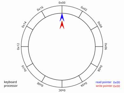
The first optimisation is to assume that the buffer is exactly one page or 256 bytes. The advantage we have there is that addressing in Z80 is 16 bits and if we’re only using the lowest 8 bits of addressing to address 256 bytes, then we simply need to align the buffer onto a single 256 byte page and then increment through the lowest byte of the buffer address to manage the pointer access.
If 256 bytes is too many to allocate to the buffer, then if we use a power of 2 buffer size, and then align the buffer within the memory so that it falls on the boundary of the buffer size, the calculation for the pointers becomes simple masking (rather than a decision and jump). Simple masking ensures that no jumps are taken, which means that the code flow or delay is constant no matter which place in the buffer is been written or read.
Note that although the number of bytes allocated to the buffer is 256, the buffer cannot be filled completely. A completely full 256 byte buffer cannot be discriminated from a zero fullness buffer. This does not apply where the buffer is smaller than the full page.
With these two optimisations in place, we can now look at three implementations of USART interfaces for the Z80 platform. These are the MC6580 ACIA , the Zilog SIO/2, and the Z180 ASCI interface. There is also the Am9511A interface, which is a little special as it has multiple independent ring buffers, and has multi-byte insertion.
Implementations
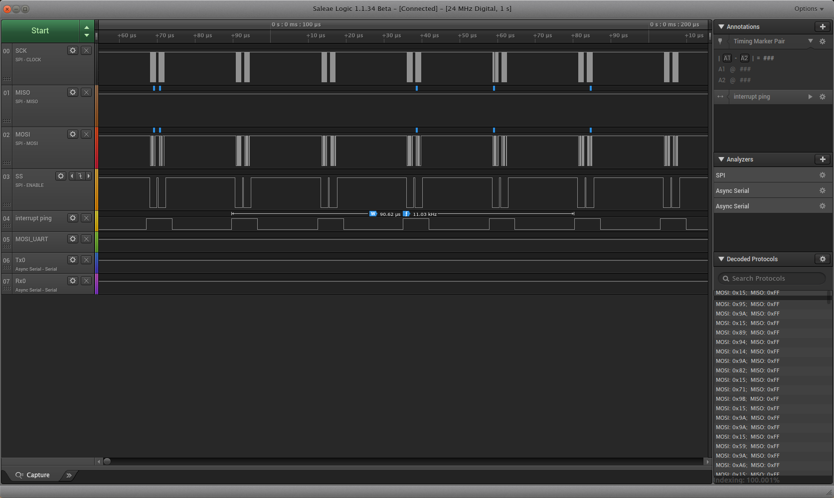
To start the discussion, let us look at the ACIA implementation for the RC2014 CP/M-IDE bios. I have chosen this file because all of the functions are contained in one file, which provides an easier overview. The functions are identical to those found in the z88dk RC2014 ACIA device directory.
Using the ALIGN key word of the z88dk, the ring buffer itself is placed on a page boundary, in the case of the receive buffer of 256 bytes, and on the buffer size boundary, in the case of the transmit buffer of 2^n bytes.
Note that although where the buffer is smaller than a full page all of the bytes in the buffer could be used, because the buffer counter won’t overflow, but I haven’t made that additional optimisation in my code. So no matter how many bytes are allocated to a buffer, one byte always remains unused.
Once the buffer is located, the process of producing and consuming data is left to either put or get functions which write to, or read from the buffer as and when they choose to. There is no compulsion for the main program flow to write or read at a particular time, and therefore the flow of code is never delayed. This is optimum from the point of view of minimising delay and maximising compute time. Additional functions such as flush, peek, and poll are also provided to simplify program flow, and init to set up the peripheral and initialise the buffers on first use.
With the buffer available then the interrupt function can do its work. Once an interrupt from the peripheral is signalled, the interrupt code checks to see whether a byte has been received. If not then the interrupt (in the case of the ACIA and ASCI) must have been triggered by the transmit hardware becoming available.
If in fact a byte has been received by the peripheral then the interrupt code recovers the byte, and checks there is room in the buffer to store it. If not, then the byte is simply abandoned. If there is space, then the byte is stored, and the buffer count is incremented. It is critical that these two items happen atomically, which in the case of an interrupt is the natural situation.
If the transmission hardware has signalled that it is free, then the buffer is checked for an available byte to transmit. If none is found then the transmit interrupt is disabled. Otherwise the byte is retrieved from the buffer and written to the transmit hardware while the buffer count is decremented.
If the transmit buffer count reaches zero when the current byte is transmitted, then the interrupt must disable further transmit interrupts to prevent the interrupt being called unnecessarily (i.e. with the buffer fullness being empty).
Multi-byte Receive
Both the SIO and ASCI have multi-byte hardware FIFO buffers available. This is to prevent over-run of the hardware should the CPU be unable to service the receive interrupt in sufficient time. This could happen if the CPU is left with its general interrupt disabled for some time.
In this situation, the SIO receive interrupt and the ASCI interrupt have the capability to check for additional bytes before continuing.
Transmit cut-through
One additional feature worth discussing is the presence of a transmit cut-through, which minimises delay when writing the “first byte”. Because the Z80 processor is relatively slow compared to a serial interface, it is common for the transmit interface to be idle when the first byte of a sequence of bytes is written. In this situation writing the byte into the transmit buffer, and then signalling a pseudo interrupt (by calling the interrupt routine) would be very costly. In the case of the first byte it is much more effective simply to cut-through and write directly to the hardware.
Atomicity
For the ring buffer to function effectively, the atomicity of specific operations must be guaranteed. During an interrupt in Z80 further interrupts are typically not permitted, so within the interrupt we have a degree of atomicity. The only exception to this rule is the Z80 Non Maskable Interrupt (NMI), but since this interrupt is not compatible with CP/M it has never been used widely and is therefore not a real issue.
For the buffer get function the only concern is that the retrieval of a byte is atomically linked to the number of bytes in the buffer.
For the put function it is similar, however as the transmit interrupt needs to be enabled by the put function atomcity is required to ensure that this process is not interrupted.
Interrupt Mode
Across the three implementations there are three different Z80 interrupt modes in play. The Motorola ACIA is not a Zilog Z80 peripheral, so it can only signal a normal interrupt, and can therefore (without some dirty tricks) only work in Interrupt Mode 1. For the RC2014 implementation it is attached to INT or RST38 and therefore when an interrupt is triggered it is up to the interrupt routine to determine why an interrupt has been raised. This leads to a fairly long and slow interrupt code.
The Z180 ASCI has two ports and is attached to the Z180 internal interrupt structure, which works effectively similarly to the Z80 Interrupt Mode 2, although it is actually independent from the Z80 interrupt mode. Each Z180 internal interrupt is separately triggered, however it still cannot discern between a receive and a transmit event. So the interrupt handling is essentially similar to that of the ACIA.
The Zilog SIO/2 is capable of being attached to the Z80 in Interrupt Mode 2. This means that the SIO is capable of being configured to load the Z80 address lines during an interrupt with a specific vector for each interrupt cause. The interrupts for transmit empty, received byte, transmit error, and receive error are all signalled separately via an IM2 Interrupt Vector Table. This leads to concise and fast interrupts, specific to the cause at hand. The SIO/2 is the most efficient of all the interfaces described here.
Multi-byte buffers
For interest, the Am9511A interface uses two buffers, one for the one byte commands, and one for the two byte operand pointers. The command buffer is loaded with actions that the APU needs to perform, including some special (non hardware) commands to support loading and unloading operands from the APU FILO.
A second Am9511A interface also uses two buffers, one for one byte commands, and one for either two or four byte operands. This mechanism in not as nice as storing pointers as in the above driver, but is required for situations where the Z180 is operating with paged memory.
I’ve revised this above solution again and do it with three byte operand (far) pointers, as that makes for a much simplified user experience. The operands don’t have to be unloaded by the user. They simply appear auto-magically…