Three Rings for the Z80

Over the past few years I’ve implemented a number of interfaces for Z80 peripherals based on the principal of the interrupt driven ring buffer. Each implementation of a ring exhibits its own peculiarities, based on the specific hardware. But essentially I have but one ring to bring them all and in the darkness bind them.

This is some background on how these interfaces work, why they’re probably fairly optimal at what they do, and things to consider if extending these to other platforms and devices.

The ring buffer is a mechanism which allows a producer and a consumer of information to do so with a timing to suit their needs, and to do it without coordinating their timing.

The Wikipedia defines a circular buffer, or ring buffer,  as a data structure that uses a single fixed-size buffer as if it were connected end-to-end. The most useful property of the ring buffer is that it does not need to have its elements relocated as they are added or consumed. It is best suited to be a FIFO buffer.

Background

Over the past few years, I’ve used the ring buffer mechanism written by Dean Camera in many AVR projects. These include interrupt driven USART interfaces, a digital audio delay loop, and a packet assembly and play-out buffer for a digital walkie-talkie.

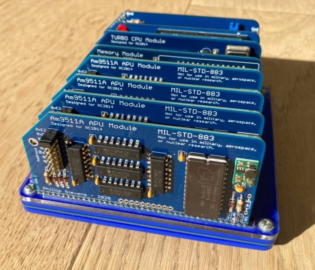
More recently, I’ve been working with Z80 platforms and I’ve taken that experience into building interrupt driven ring buffer mechanisms for peripherals on the Z80 bus. These include three rings for three different USART implementations, and a fourth ring for an Am9511A APU.

But firstly, how does the ring buffer work? For the details, the Wikipedia entry on circular buffers is the best bet. But quickly, the information (usually a byte, but not necessarily) is pushed into the buffer by the producer, and it is removed by the consumer.

The producer maintains a pointer to where it is inserting the data. The consumer maintains a pointer to where it is removing the data. Both producer and consumer have access to a count of how many items there are in the buffer and, critically, the act of counting entries present in the buffer and adding or removing data must be synchronised or atomic.

8 Bit Optimisation

The AVR example code is written in C and is not optimised for the Z80 platform. By using some platform specific design decisions it is possible to substantially optimise the operation of a general ring buffer, which is important as the Z80 is fairly slow.

The first optimisation is to assume that the buffer is exactly one page or 256 bytes. The advantage we have there is that addressing in Z80 is 16 bits and if we’re only using the lowest 8 bits of addressing to address 256 bytes, then we simply need to align the buffer onto a single 256 byte page and then increment through the lowest byte of the buffer address to manage the pointer access.

If 256 bytes is too many to allocate to the buffer, then if we use a power of 2 buffer size, and then align the buffer within the memory so that it falls on the boundary of the buffer size, the calculation for the pointers becomes simple masking (rather than a decision and jump). Simple masking ensures that no jumps are taken, which means that the code flow or delay is constant no matter which place in the buffer is been written or read.

Note that although the number of bytes allocated to the buffer is 256, the buffer cannot be filled completely. A completely full 256 byte buffer cannot be discriminated from a zero fullness buffer. This does not apply where the buffer is smaller than the full page.

With these two optimisations in place, we can now look at three implementations of USART interfaces for the Z80 platform. These are the MC6580 ACIA , the Zilog SIO/2, and the Z180 ASCI interface. There is also the Am9511A interface, which is a little special as it has multiple independent ring buffers, and has multi-byte insertion.

Implementations

To start the discussion, let us look at the ACIA implementation for the RC2014 CP/M-IDE bios. I have chosen this file because all of the functions are contained in one file, which provides an easier overview. The functions are identical to those found in the z88dk RC2014 ACIA device directory.

Using the ALIGN key word of the z88dk, the ring buffer itself is placed on a page boundary, in the case of the receive buffer of 256 bytes, and on the buffer size boundary, in the case of the transmit buffer of 2^n bytes.

Note that although where the buffer is smaller than a full page all of the bytes in the buffer could be used, because the buffer counter won’t overflow, but I haven’t made that additional optimisation in my code. So no matter how many bytes are allocated to a buffer, one byte always remains unused.

Once the buffer is located, the process of producing and consuming data is left to either put or get functions which write to, or read from the buffer as and when they choose to. There is no compulsion for the main program flow to write or read at a particular time, and therefore the flow of code is never delayed. This is optimum from the point of view of minimising delay and maximising compute time. Additional functions such as flushpeek, and poll are also provided to simplify program flow, and init to set up the peripheral and initialise the buffers on first use.

With the buffer available then the interrupt function can do its work. Once an interrupt from the peripheral is signalled, the interrupt code checks to see whether a byte has been received. If not then the interrupt (in the case of the ACIA and ASCI) must have been triggered by the transmit hardware becoming available.

If in fact a byte has been received by the peripheral then the interrupt code recovers the byte, and checks there is room in the buffer to store it. If not, then the byte is simply abandoned. If there is space, then the byte is stored, and the buffer count is incremented. It is critical that these two items happen atomically, which in the case of an interrupt is the natural situation.

If the transmission hardware has signalled that it is free, then the buffer is checked for an available byte to transmit. If none is found then the transmit interrupt is disabled. Otherwise the byte is retrieved from the buffer and written to the transmit hardware while the buffer count is decremented.

If the transmit buffer count reaches zero when the current byte is transmitted, then the interrupt must disable further transmit interrupts to prevent the interrupt being called unnecessarily (i.e. with the buffer fullness being empty).

Multi-byte Receive

Both the SIO and ASCI have multi-byte hardware FIFO buffers available. This is to prevent over-run of the hardware should the CPU be unable to service the receive interrupt in sufficient time. This could happen if the CPU is left with its general interrupt disabled for some time.

In this situation, the SIO receive interrupt and the ASCI interrupt have the capability to check for additional bytes before continuing.

Transmit cut-through

One additional feature worth discussing is the presence of a transmit cut-through, which minimises delay when writing the “first byte”. Because the Z80 processor is relatively slow compared to a serial interface, it is common for the transmit interface to be idle when the first byte of a sequence of bytes is written. In this situation writing the byte into the transmit buffer, and then signalling a pseudo interrupt (by calling the interrupt routine) would be very costly. In the case of the first byte it is much more effective simply to cut-through and write directly to the hardware.

Atomicity

For the ring buffer to function effectively, the atomicity of specific operations must be guaranteed. During an interrupt in Z80 further interrupts are typically not permitted, so within the interrupt we have a degree of atomicity. The only exception to this rule is the Z80 Non Maskable Interrupt (NMI), but since this interrupt is not compatible with CP/M it has never been used widely and is therefore not a real issue.

For the buffer get function the only concern is that the retrieval of a byte is atomically linked to the number of bytes in the buffer.

For the put function it is similar, however as the transmit interrupt needs to be enabled by the put function atomcity is required to ensure that this process is not interrupted.

Interrupt Mode

Across the three implementations there are three different Z80 interrupt modes in play. The Motorola ACIA is not a Zilog Z80 peripheral, so it can only signal a normal interrupt, and can therefore (without some dirty tricks) only work in Interrupt Mode 1. For the RC2014 implementation it is attached to INT or RST38 and therefore when an interrupt is triggered it is up to the interrupt routine to determine why an interrupt has been raised. This leads to a fairly long and slow interrupt code.

The Z180 ASCI has two ports and is attached to the Z180 internal interrupt structure, which works effectively similarly to the Z80 Interrupt Mode 2, although it is actually independent from the Z80 interrupt mode. Each Z180 internal interrupt is separately triggered, however it still cannot discern between a receive and a transmit event. So the interrupt handling is essentially similar to that of the ACIA.

The Zilog SIO/2 is capable of being attached to the Z80 in Interrupt Mode 2. This means that the SIO is capable of being configured to load the Z80 address lines during an interrupt with a specific vector for each interrupt cause. The interrupts for transmit empty, received byte, transmit error, and receive error are all signalled separately via an IM2 Interrupt Vector Table. This leads to concise and fast interrupts, specific to the cause at hand. The SIO/2 is the most efficient of all the interfaces described here.

Multi-byte buffers

For interest, the Am9511A interface uses two buffers, one for the one byte commands, and one for the two byte operand pointers. The command buffer is loaded with actions that the APU needs to perform, including some special (non hardware) commands to support loading and unloading operands from the APU FILO.

A second Am9511A interface also uses two buffers, one for one byte commands, and one for either two or four byte operands. This mechanism in not as nice as storing pointers as in the above driver, but is required for situations where the Z180 is operating with paged memory.

I’ve revised this above solution again and do it with three byte operand (far) pointers, as that makes for a much simplified user experience. The operands don’t have to be unloaded by the user. They simply appear auto-magically…

Yet Another Z180 (YAZ180 v2)

Testing on the YAZ180 v1 , shown below, is now complete. I don’t want to use it for further driver and platform development, because the PLCC socket for the 256kB Flash is becoming worn-out.

It will continue to operate as an augmented Nascom Basic machine, with an integrated Intel HEX loader (HexLoadr) supporting direct loaded assembler or C applications.

img_0626

YAZ180 v1 at full configuration.

The new PCB for the YAZ180 v2 has been ordered.

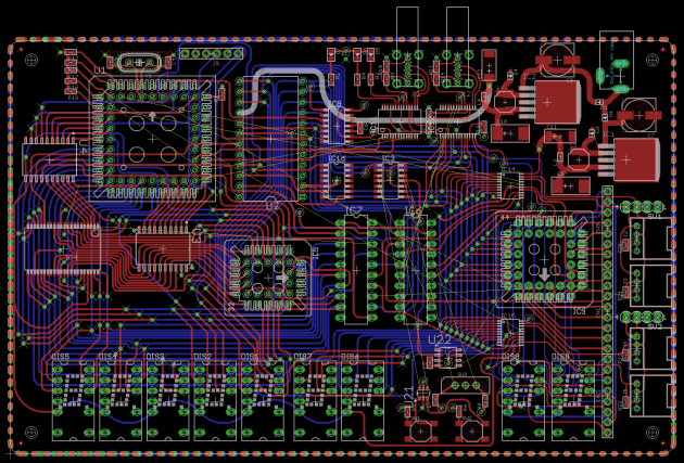
These are some screenshots of the new PCB.


Update

Pi Day, March 14 2017.

After dwelling on the fact that the V2 PCB was really just a clean up the V1 PCB, with no additional features, I decided not to build the beautiful new PCBs that arrived today.

But rather, to create a new PCB with additional features.


New Features

When I originally designed the YAZ180 the breakout for the 82C55 was simply an interim design, to enable me to test the board. I was thinking of making an Arduino style pin-out, or something along those lines. But this is something much better.

Recently, after reading Paul’s page on interfacing an IDE drive to an 8051 microprocessor with the 82C55, I decided that adding IDE to the YAZ180 was a must-have feature.

So there is a new connector on the YAZ180 to break out the 82C55 pins, in IDE 44-pin 2mm format. I have not followed the design provided by Paul exactly. I’d note that his design and the earlier design by Peter Fraasse were specialist designs, which don’t support the generalised usage of the 82C55 chip, beyond the IDE functionality.

By the above statement I mean that in Mode 1 and Mode 2 for Port A and Port B, the PC2, PC4, and PC6 pins of the 82C55 device are designated registered strobe input pins /STB in input mode, or peripheral acknowledge /ACK in output mode. If an inverting output buffer is connected on these lines, then the registered input and output mode capability is lost. This would restrict the functionality of the 82C55 to simply Mode 0, being the mode that is used to create the IDE functionality.

As I’ve connected the three IDE address selection pins to PC2, PC4, and PC6, and these pins are not passed through an inverting buffer in the design, it is possible to use the 82C55 in any of its modes, and therefore to use the IDE 2.5″ 44-pin form factor to connect the YAZ180 82C55 ports to extension PCBs of any type or design.

As a connected IDE drive or other extension board may need to interrupt the CPU, I have connected the IDE INTRQ pin to the remaining inverting buffer to provide an input to the CPU on /INT0. As the /INT0 (or actually the INTRQ) input terminates on the IDE header, either a IDE drive through INTRQ, or either of the two 82C55 INTR pins, PC3 or PC0, can originate the interrupt.

I have reconfigured the Am9511A-1 to use the /NMI interrupt, as previously the /INT0 was configured.

The new YAZ180 v2 PCB has been ordered. YAZ180_v2_Schematic.

Happy Pi Day.

Update – RetroChallenge Day 1

I’ve decided to enter the RetroChallenge 2017/04 and my challenge is to read and write to an IDE drive using the newly configured IDE interface on the YAZ180v2. But before I can write the code for the IDE interface, there’s a bit of building and testing that needs to be done.

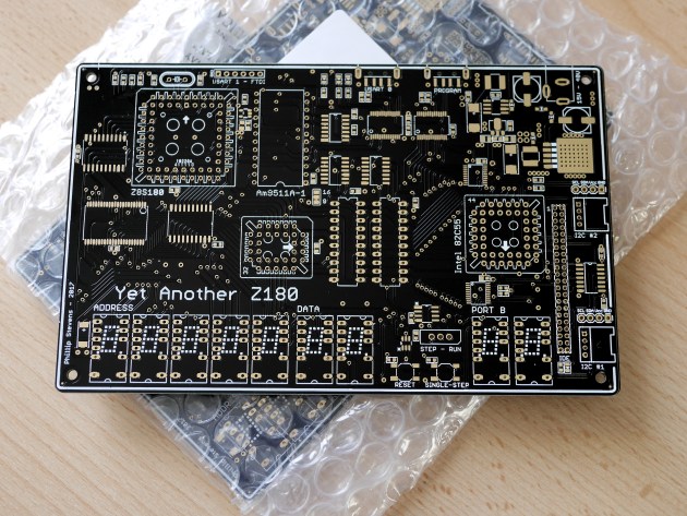
The new PCBs arrived a few days ago, and they look great. But Arduino Day and the first day of the RetroChallenge 2017/04, 1st April, seemed like a good day to lay them out.

P1080754

New PCBs. 2oz Copper, 2mm thick. Opulent.

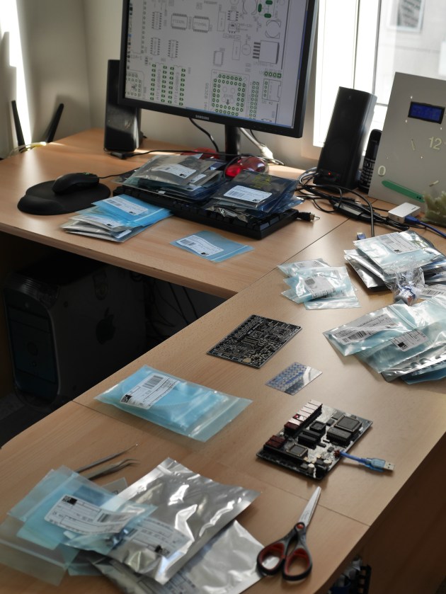
I was hoping to lay build several boards at once, but somehow I forgot that there was only one RAM and one FT245 device in my component stocks. That means that I had to satisfy myself with just one board for now.

Note the suitably Retro PowerMac (circa 2001) driving the layout guide screen.

P1080755

Adhoc Workspace

This is the board just before cooking. Respect to anyone who notices the substantial noob layout mistake. Anyway, after a small smokey explosion, everything was rectified.

P1080758

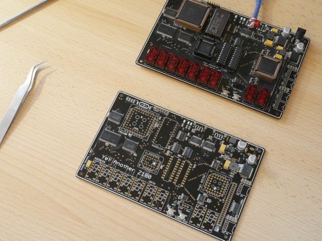
Two YAZ180 versions, side by side.

This is the finished build of the YAZ180 v2. Looks very tasty. Retro goodness.

P1080761.JPG

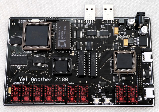
Fully populated YAZ180 v2 PCB.

I’m still working on fixing an issue with my code, which I noticed when experimenting with the Am9511A APU, and inserting an Interrupt Jump Table. Basically, I’m getting jumps to odd or  random locations, which is detected buy filling unused locations with 0x76, the HALT, OpCode. The most common address where the HALT is executed at is 0x00C3.

Previously, I’d been filling unused locations with 0xFF, the RST 38H OpCode shared with the INT0 location 0x0038, which was causing the APU to be triggered inappropriately. This issue has me snookered. I can’t move on, in the software sense, until it is resolved .


This slideshow requires JavaScript.

Update – RetroChallenge Day 8

Well this week was one of the most frustrating weeks ever, in terms of time spent vs. results obtained.

There are two major projects in hand. 1. Getting the YAZ180 v2 running, and 2. resolving the software issue plaguing my initialisation code.

Hardware issues

Bringing up a new piece of hardware is never easy. Initially, nothing can be trusted to work, and everything needs to be checked against the design, and then even the design checked for correctness. Bringing up the YAZ180 v1 was very time consuming, because I had to develop the PLD design during the process, as well as checking that all the hardware was sorking as it should. I thought that bringing up the YAZ180 v2 would be easy. Just solder it together and win. But it has not been so simple.

Essentially, after a week of working on this every evening, I don’t know why it is not working correctly. All the standard things, volts, clock, stuck address and data lines, etc are all working correctly. But it still doesn’t work. And, it may not be just one thing that is wrong, but if anything is not perfect it just won’t work.

After a few days of testing, I found that I’d programmed the PLD devices with an old version of the CUPL code. Nearly right, but not exactly right. Once I’d isolated that issue, by ensuring the new GAL devices worked perfectly in the V1 board, I thought it would be enough. But no. There’s still something wrong.

My current thought is that somehow, either electro-static damage or heat damage, the RAM is unreliable. But, I’m not sure enough of this to unsolder the RAM device and replace it. I’ll be spending this weekend on resolving this problem.

Software issues

Because of the effort I’ve been putting into resolving the hardware issues, I’ve not been able to solve the software issue apparent in the YAZ180 initialisation and serial code. I’ve documented the issue on Github.

My lesson learned is NOT to fill unused memory with 0xFF bytes. This causes RST 38H jumps to the INT0 location when the PC is incorrectly loaded, and can be very distracting. Best to fill unused memory with either 0x76 HALT bytes, to see where things became broken, or with 0xC9 RET bytes to just float over the underlying issue.

I’ll need to fix this properly, but it has consumed several weeks of effort, and I’m not much closer to resolution.

Update – RetroChallenge Day 10

The weekend was unkind, but today some new eyes (literally) have brought successes.

Hardware Issues

After doing quite a bit of further testing, I’m fairly sure that I’ve damaged the RAM and will need to replace it. So, I’ve ordered a hot-air solder gun. Should have had one for a long time. Finally, I’ve got a round-‘tuit. I’ll have to order some replacement components too, which will result in being able to make additional boards as well.

Software Issues

Finally, I’ve resolved my issue. What we had here was a classic “failure to understand”. Somewhat embarrassed to leave this here for Internet eternity.

  • Z80 vectors are supported by a JUMP table.
  • Z180 vectors are supported by an ADDRESS table.

Insert JP instructions into an address table and you will have a very very bad day.

Or in my case, quite a few of them.

This issue cost so much time. But at least on the up side, I’ve written robust Z80 and Z180 vector tables, improved my ASCI code, and cleaned up initialisation code, in trying to track this down.

Also finally, I now understand. Which is the entire point, anyway.

Update – RetroChallenge Day 17

Following up on the success of last weekend, I was hoping to have a lot of achievement to write about today. Unfortunately, it has been a grind this week too.

I have been distracted back into the original project that unearthed my previous software problem, and led me along the path to getting a much better understanding of the Z180 CPU, and then solving the issue. The original project was building an interrupt driven driver for the Am9511A-1 Arithmetic Processing Unit.

I’ve spent pretty much the past week on this code, and digging through it with a fine tooth comb. I’m now of a belief that my Am9511A driver code is correct, but my hardware is not correct and may never be correct.

The issue lies with the requirement for the Am9511A to have the Address lines and Chip Select signal remain valid for 30ns following raising of the Write signal. Unfortunately, the Z180 only maintains valid address lines for 5ns following Write. This means that writing to the AM9511A APU is very much a hit and miss affair, with miss being the most likely outcome. I’m still thinking about ways to bodge this to work. But, I think that it may just be too hard to get the old APU to work with a modern CPU. More on this later.

This week I’ll be working on the PaulMon IDE code, and migrating it from 8051 to Z80 nomenclature, and trying to get it to compile.

Update – RetroChallenge Day 21

Well the last couple of days have been exciting, as I found a way to make the Am9511A APU work. A hint from a fellow competitor (on working with the MC6809 CPU) inspired me to look further for information on options to fix the hardware interface.

The Z180 E CLOCK

The Z180 has an almost undocumented feature, called the E Clock. Yes, it is documented in datasheet that it exists, but there’s no real background that I can find as to why it exists, except that is for a Secondary Bus Interface. This pin and signal doesn’t exist on the Z80, for example. Anyway, since it has the same name as a signal on the MC6809, I thought it might be worth looking at it. It turns out that the E Clock provides a shortened version of the WR and RD cycles. Which is exactly what we need.

One caveat however, when running at doubled PHI rates (i.e. 1:1 PHI – CLK) the shortening of the E Clock signal is not sufficient to drive the APU successfully. At 18.432MHz, the PHI/2 timing is 27ns. Therefore, the minimum of 30ns between release of WR and CS is not always held. This means that we’ll need to keep the PHI at half CLK whilst using writing data into the APU. In practice this means that using the APU requires we cut the CPU clock by 50% or PHI/2 being 57ns, to ensure the trailing 30ns is provided.

Anyway. Good news. With the revised timing, the Am9511A-1 is working.

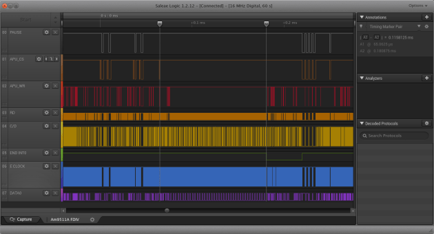
Am9511A FDIV

Am9511A APU Floating Divide in 115us

The E Clock is not an inverted signal, so to generate the active low APU_WR signal we have to first invert it, then OR it with the WR signal. For the purposes of testing, I’ve got a little breadboard with a GAL on the side, but later I’ll build a new PCB and add in a SN74LVC1G97 little logic device to provide the APU_WR signal.

Am9511A FDIV PUPI

Am9511A APU FDIV PUPI command interval 128us

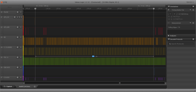
Am9511A FDIV PHI6 Cycles

Am9511A APU FDIV in 179 Phi/6 Clock cycles

So now we see the Am9511A APU FDIV floating point divide takes about 101us to 115us when running at 1.536MHz, or from the datasheet 154 to 184 clock cycles. In 101us, the Z180 CPU at 36.864MHz produces 3,723 cycles. To produce a floating point divide using the Lawrence Livermore Library requires about 13,080 cycles, according to the AM9511A Floating Point Processor Manual by Steven Cheng. Therefore, we are still substantially faster than antique software on a modern Z180!

Update – RetroChallenge Wrap Up

Well the month of RC2017/04 didn’t go quite as planned. My original intention was to have the YAZ180v2 working very quickly, then get straight down to porting Paul’s IDE code from 8051 to Z180 to get the new IDE interface working. But, there were several speed bumps along the way.

Gaining an education

Since I just started on this whole Z80 processor and assembly language programming thing a few months ago, I don’t have a long history of coding to fall back on. I had written some code for the Z80 in the RC2014 hardware, which I then tried to use on the Z180 in the YAZ180. But, there is a subtle difference in “generation” between the way the interrupt vectors work across the two machines. Obvious, once you know about it but a real “time killer” if you don’t.

Firstly, filling unused space in your assembly program with 0xFF is a very dangerous thing to do in Z80 assembler, particularly if you don’t understand that 0xFF is the op code for RST38, which is a single byte jump to the same location as the Interrupt 0 in IM1 mode. It would make more sense to fill the unused space with 0x76, which is the HALT instruction, to trap an unexpected program counter value.

Look before you leap

Secondly, the interrupt vectors on the Z80 were designed to contain code, and the PC is just loaded with the address of the vector, and execution begins from there. So for an INT0 (or RST38) execution begins from 0x0038. But, the interrupt vectors on the Z180 are designed to hold an address. The difference being that an interrupt will load the PC with the contents of the two bytes at the vector, and then begin execution from there. I think this difference is a sign of the generational difference between the two implementations. One of the clearest differences I can find, anyway.

Timing is everything

One of the goals for the YAZ180 is to bring some old chips back to life, in a modern platform. Along with the TIL311, GAL16v8, and 82C55 devices, the Am9511A holds pride of place as the very first arithmetic processing unit ever made. I’ve invested far too much time in getting the Am9511A to work, but it is important to me that my project can make it work.

I believed that I had devices that were specified to run at 3MHz but which in fact didn’t. That may be incorrect. More likely was that I wasn’t driving them properly, because my timing was out. I will need to go back and test them all again.

Here the issue is that the Am9511A requires extended validity of data and chip select signal, following the validity of the write signal. At least 30ns is required. This is not provided by the Z180 in its normal timing, although in the configuration I have it, coincidentally because I’d buffered the data bus, it is nearly right. Only the chip select line was being incorrectly handled.

I was nearly giving up but then a tweet from a fellow RC2017/04 competitor gave me the inspiration to look further. It turns out that the Z180 has a secondary I/O timing signal called the E Clock. This signal is not present on the Z80, and as I didn’t understand its purpose I’d left it unconnected in the YAZ180.

Whilst the Zilog datasheets on the Z180 completely gloss over the purpose of the E Clock signal, by simply not mentioning it, the original Hitachi 64180 datasheets do mention it. The original purpose of the E Clock signal was to provide timing for “a large selection of 6800 type peripheral devices” including the “Hitachi 6300 CMOS series (6221 PIA, 6350 ACIA, etc) as well as the 6500 family devices”.

In summary, the E Clock provides a signal that is half a T cycle shorter than the write signal. It means that gating the write signal with the E Clock would allow me to release the APU write signal sufficiently early to maintain the extended chip select timing required. Basically, the APU won’t operate with a Z180 T Cycle any less than 60ns, or 16.6MHz. So in my implementation, the PHI clock will need to run at half speed or 9.234MHz, whilst the Z180 is using the Am9511A. Unless I cook up another plan.

Zapped

And the final note from this month is that I believe my very poor ESD protocol has led to the destruction of the SRAM on my YAZ180v2. Therefore I had to desolder it (and it looked so nicely done) to remove it, and order some new components.

Ordering new components is always a bit of a hurdle for me. I’ve collected quite a few things that I don’t use, so I tend to ration myself on purchases vs. progress. Finally, at the end of the month I ordered more components to build further YAZ180 boards, and some spare SRAM to enable me to repair the one I have made already.

It continues to amaze me just how much difference there is in the cost to build an Arduino AVR board (basically just a chip at the most essential level), vs something like the YAZ180. The YAZ180v2 bill of materials, excluding specials like the GAL16V8D, TIL311, and Am9511A devices that I have to find of eBay, comes to over $150 Australian!!! We need to export more coal, to get the AUD dollar back up there!

And that’s it for my RC2017/04 month. Soon as the parts arrive I’ll be completing the YAZ180v2, and then testing the IDE interface. I hope that will be done before the end of 2017/05.

Update – Post RetroChallenge

Well good news. The only issue was a bad solder joint on the new SRAM chip. Now the YAZ180v2 is running, and I can get onto translating the IDE code from 8051 to Z80.

IMG_0698

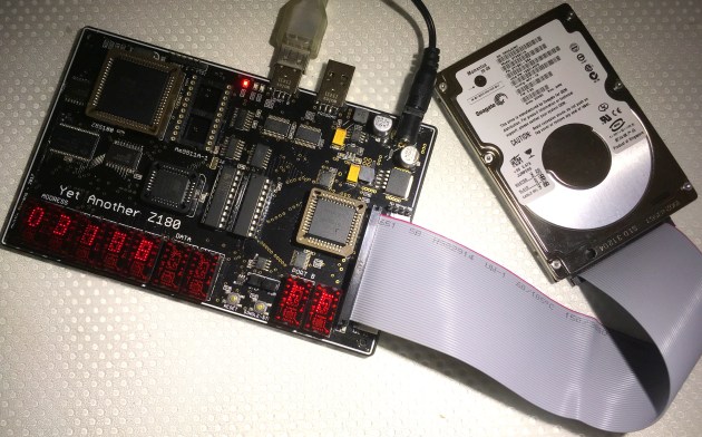
YAZ180 with IDE drive attached.

I’ve sourced code from both PJRC in 8051 mnemonics for an 8255 PIO and from Retroleum in Z80 mnemonics for an 8 bit interface. Between the two of them, together with the examples from the OSDev Wiki, it should be easy to make a fairly robust implementation. And, on May 18th, the driver code was finally working.

Next activity is to integrate this into the z88dk, and then using the FAT-FS code from Elm ChaN, get the disks properly working.

Update – August 2017

Over the past few months progress has been made on various fronts with the YAZ180v2. Firstly, the IDE interface is fully working, and has been integrated into z88dk. Also, the issues with the Am9511A-1 APU have been resolved, and a working driver has been integrated into z88dk. While I still have to revise the C interface for these two pieces of code, because I’m still learning this, the development work is now done.

I am particuarly happy about getting the Am9511A APU working, as this was causing me the most technical difficulty, and stretched my understanding the most. I’m also happy that the capability in the Am9511A seems to be realised through performance improvements in arithmetic computation.

Over the coming months, I hope to resolve the remaining untested components in the YAZ180. These include the parallel programming interface, to allow the YAZ180 to be “cold loaded”, to protect against bricking the system, if a user doesn’t have a EEPROM or Flash writer. I’m still in two minds abou this feature, as the cost of the FT245 device and USB socket is about the same as a stand alone EEPROM writer, and the parallel programming interface consumes space that could be otherwise used for an SPI or USB interface, for example.

I also need to test the I2C interfaces, and debug the driver that I wrote back in May (still unused) to complete the feature set.

With this done, I’ve now done a new minor revision of the hardware, to clean up the issues that have been noted over the past months.

Open Issues

  • APU – Gate E clock with WR to produce shortened APU WR
  • NMI – remove this from the APU, and terminate high. Not CP/M compatible.
  • INTO – reconnect it to the APU.
  • 5V – Power inductor spacing.

Update – October 2017

Well, I fixed the issues and then convinced myself that there needed to be Yet Another feature added to the YAZ180, before I signed it off. So now, the v2.1 board has access to the Internet through an ESP-01S AT interface.


This slideshow requires JavaScript.

I sell on Tindie

Building up this new board will be November and December’s activity, together with building a complete YABIOS (Yet Another BIOS) to make use of all of the features packed into the YAZ180 board. I’ll be picking the best bits, IMHO, from the Cambridge Z88, ZX Spectrum, and CP/M 2.2 – ZSystem to build a banking capable YABIOS, supporting 1MByte of address space.

Update – August 2018

I seriously need to write another blog on the YAZ180. But I guess the Github commits just speak for themselves. There are only three things left on the to-do list. 1. finish the firmware loading program. 2. rewrite the I2C interface. And 3. implement FreeRTOS as a hypervisor allowing multiple 60kB applications to run simultaneously.

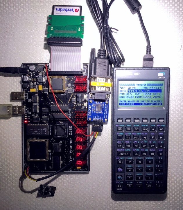
Here’s a picture of an application, which was one of the early drivers for building the YAZ180, a mass-storage platform for my HP48 calculator.

IMG_1572

YAZ180 communicating with HP48 using Kermit on ASCI1 (TTY).

Characterising Am9511A-1 APU

I’ve built two hardware solutions supporting the AM9511A APU. Partly for historical enjoyment, and partly because the AM9511A is actually still faster at floating point and 32-bit long arithmetic than “modern” Z80 devices.

I’ve built a Z180 based board, the YAZ180, which runs the AM9511A at 2.304MHz. And I’ve built an APU Module for the RC2014 platform, which runs the AM9511A at 2.4576MHz. Both of these solutions are supported by the z88dk am9511 maths library and platform drivers for Z80, Z180, and 8085 CPUs.

To compare the performance, for example, from the Am9511/Am9512 Floating Point Processor Manual we have some comparison tables. On average the Am9511A APU (at 1.966MHz) produces a hardware floating point divide in 165.9 cycles (of a 2MHz 8080 processor). Converted to my YAZ180 Am9511A implementation (at 2.304MHz), we have the equivalent in 141.5 cycles of the 2MHz 8080. Converted to best case modern Z180 terms (overclocked to 36.864MHz) this is 2,609 CPU cycles to return a hardware floating point divide.

To produce an equivalent software floating point divide, using the equivalent vintage LLL floating point library, requires 13,080 cycles.

This means that floating point on the 40 year old AM9511A-1 APU is still 5.0 times faster than an overclocked Z180 running antique 8080 code. Sweet!

Testing

I’m integrating an Am9511A-1 APU device into my YAZ180 build. The basic device is capable of operating at 3MHz. But, I’ve found that driving one sample at 3.072MHz doesn’t work. But, it works fine at 1.536MHz, and at 2.304MHz.

This one example has 83.33ns delay between RD or WR and PAUSE signal being operated. This means that it should comfortably operate with the minimum of one wait state when the Z8S180 is running with a 18.432MHz bus.

And, I’ve got to say that these devices run hot… OHS issue hot. There is a reason they are provided in a ceramic package. They sink 70mA at 12V plus another 70mA at 5V, and all that energy has to go somewhere.

Originally, I had created the timing for the Am9511A-1 is generated by dividing the Z8S180 18.432MHz system clock by 6. The divide FCPU by 6 for FAPU CLK 3.072MHz is done with a SN74LS92N device. And for test purposes, the Z8S180 is also half rate clocked at 9.216 MHz, producing 1.576MHz for the APU.

img_0620

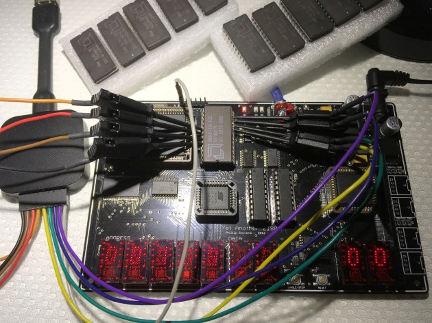
YAZ180 Test Rig – Am9511A-1

Initial Testing

The test is initially pretty simple, really just a proof of life. Will they properly push and pop data at 3.072MHz?

If not, then I’ll need to redesign the YAZ180 to operate the Am9511A-1 at a lower APU clock. But, if my initial samples are just not the up to specification, then they can be secondary devices.

Ok, now what kind of devices have I got to hand, and lets see what the results are…

Front Serial ID Country & Rear ID 3.072MHz 1.576MHz
239KH2Z Malaysia 9237FP Fail Pass
301MBZP Malaysia 9252CP Fail Pass
3368YF8 Malaysia 9335CP Fail Pass
348W76S Malaysia 9347DP Fail Pass
921BDIV Philippines 8917WM Fail Pass

Kind of boring really. Pretty clear that AMD oversold the capability of its Am9511A-1 to run at 3MHz. Or, I’m not feeding them with the correct timing.

I’ll need to redesign the YAZ180v2 to provide a divided by 8 clock at 2.304MHz, and cross my fingers that they work at that clock rate.

Update September 2017

Following a substantial investment in testing of the solution in April and August, I’ve finally got a working system that can reliably use the Am9511A-1 to produce computational results.

The main issue was described in the Retro Challenge period. The Z180 CPU I/O timing is slightly different to the Z80, in that it doesn’t provide any interval between the WR/RD deselection and the CS deselection. For most peripheral devices this isn’t a problem, but for some it causes them not to work. Hitachi recognised this problem, and provided a shortened I/O signal called the “E Clock”, which can be gated together with the WR/RD signals to gain the timing desired.

The Am9511A doesn’t require the RD signal to rise before the CS signal. Its TRCS time is 0ns. However it does require the WR signal to rise 60ns (or for Am9511A-1 30ns) before the CS signal. This can be achieved by gating the WR signal together with the E Clock signal. The Z180 E Clock is 1/2 a Phi cycle shorter than the WR signal during I/O instructions.  Therefore provided that the Z180 Phi is slow enough, then the required timing can be held. At 18,432MHz, the Z180 Phi signal is 54ns long, and therefore 1/2 Phi is 27ns, which is too short to work consistently. However, the Z180 can halve its Phi speed easily, and simply by changing the CMR register the Phi clock can be reduced to 9.216MHz, which in turn gives us (theoretically) 54ns TWCS for the Am9511A-1.

In practice gating the WR signal through the E Clock provides 41ns for TWCS, which is enough to work reliably with Am9511A-1 devices.

However, as the Am9511A-1 timing is derived from the Z180 clock (divided by 8), running Phi at 9.216MHz means that the APU is in turn under clocked to 1.152MHz. We can avoid this waste of capability, by managing the Z180 clock precisely during the command interrupt generated by the Am9511A-1. On entry to the interrrupt, we reduce the Phi to allow commands (TWCS) to work, and on exit from the interrupt we return the Phi to its original setting of 18.432MHz (and the APU to 2.304MHz). This also conveniently avoids having to modify the Z180 ASCI code to manage serial communications in the light of the reduced system clock.

I have also tested the Am9511A-1 using this revised WR to CS timing, with my original clocking of divide by 6 from Z180 system clock, or 3.072MHz, and it doesn’t work. This means that we actually do need to stay within the specification, and not overclock the APU.

z88dk Driver

The z88dk supports the YAZ180 platform, so I have added a driver for the Am9511A into the device folders. The driver is based on an interrupt driven model. As noted in the Am9511A Processor Manual, there are 4 different models that can be adopted.

The Am9511A Pause signal is connected to the Z180 Wait signal, so if the CPU generates a request that requires time to fulfil, then the APU will cause the CPU to Wait by signalling Pause. Clearly this means that the CPU cannot do anything while it is in Wait mode. This model of working is called Demand Wait, and it provides the fastest APU response, but doesn’t support using the CPU effectively.

The APU status register can be read without the APU causing a Pause response. Therefore the CPU can poll the APU by reading the status register. In this situation the CPU can continue profitably, but response to APU requirements (for new operands, or commands) is limited to the polling rate. As different APU commands can be completed in different times, the optimal polling time can be difficult to calculate.

The APU End signal can be connected to a CPU interrupt, and in the case of the YAZ180 it is connected to the NMI, which is then triggered at the end of each command, when the APU is ready to receive a new command. If the APU commands are buffered in advance, then using this interrupt mechanism the APU can complete a long sentence of commands “autonomously” and in parallel to the CPU activities, interrupting only when it needs to load a new command. This is the mechanism used in the z88dk driver.

Some ideas for creating an optimal interrupt driven driver for the Am9511A were inspired by reading “An Efficient Software Driver for Am9511 Arithmetic Processor Implementation”, B. Furht and P. Lee, 1984.

The final driver option is to connect the APU Service Request signals to the CPU DMA interface. In the YAZ180 these hardware signals are connected, and if desired a DMA enabled driver could be written to take advantage of this interface. However as only 4 bytes of information can be transferred in each load or unload command, at face value there seems to be little advantage in building a DMA software interface.

The C interface for the Am9511A driver supports direct access to the Am9511A, like the asm driver, and hopefully it can be integrated into the z88dk math library options, to support transparent usage of the APU where it exists.

Currently, some simple C interface code is now available on z88dk, which allows us to do performance testing.

Performance Testing

A simple test of seeking prime numbers exercises the floating point divide and 32 bit fixed point divide. This “brute force” method is not optimised for the APU as 4x 32 bit numbers must be loaded into the APU, but only two divides and a subtraction are done, for each calculation cycle. During the operand loading process, the CPU must also be slowed down to half rate, but since this is during an non-maskable interrupt there is little effect on the overall system.

So, some comparisons. First using Nascom Basic, we have a baseline, for seeking 1000 prime numbers.

20 PRINT "LIMIT";
30 INPUT L
40 FOR N = 3 TO L
50    FOR D = 2 TO (N-1)
60      IF N/D=INT(N/D) THEN GOTO 100
70    NEXT D
80    PRINT N;
90    GOTO 110
100   PRINT ".";
110 NEXT N
120 END

200 REM 124.7 Seconds (hand timed) - Z180 36.864MHz - Nascom Basic

Adding the Am9511A to the calculation, by doing the inner loop in assembly and calling the APU for the divide and subtract duties, does speed things up.

20  PRINT "LIMIT";
30  INPUT L
40  FOR N = 3 TO L
50    IF USR(N) = 0 THEN GOTO 100
80    PRINT N;
90    GOTO 110
100   PRINT ".";
110 NEXT N
120 END

200 REM 90.4 Seconds (hand timed) - Z180 36.864MHz - Nascom Basic

This is interesting, as the Am9511A is running at 2.304MHz (straight out of 1977), yet it is STILL faster than software on a 36.864MHz Z180.

Now, what happens when using the z88dk, to do the calculation in C?

void main(void)
{
  static signed long l, n, d;
  printf("Limit: ");
  scanf("%ld", &l);
  for (n = 3; n != l; ++n)
  {
    for (d = 2; d != (n-1); ++d)
      if ((float)n/(float)d == n/d) break;
    if (d == (n-1))
    printf("%ld", n);
      else
    printf(".");
  }
}

// 67.8 Seconds (hand timed) - Z180 36.864MHz - z88dk sdcc_iy
// 62.7 Seconds (hand timed) - Z180 36.864MHz - z88dk newlib

// zcc +yaz180 -subtype=basic_dcio -vn -SO3 -lm -clib=sdcc_iy --max-allocs-per-node200000 primesC.c -o primesC -create-app
// zcc +yaz180 -subtype=basic_dcio -vn -SO3 -lm -clib=new primesC.c -o primesC -create-app

Using the assembly math routines in z88dk is now the fastest solution. But, we’d expect C to be faster than Basic. What happens if we do the divides and subtractions in the Am9511A. That’s why we’re here.

void main(void)
{
  static signed long l, n, d, r;

  apu_reset( (void *) 0x2021 ); //INITIALISE THE APU with the NMI VECTOR ADDRESS

  printf("Limit: ");
  scanf("%ld", &l);

  for (n = 3; n != l; ++n)
  {
    for (d = 2; d != (n-1); ++d)
    {
      apu_cmd_ld( &n,   APU_OP_ENT32);
      apu_cmd_ld( NULL,     APU_OP_FLTD);
      apu_cmd_ld( &d,   APU_OP_ENT32);
      apu_cmd_ld( NULL,     APU_OP_FLTD);
      apu_cmd_ld( NULL,     APU_OP_FDIV);
      apu_cmd_ld( &n,   APU_OP_ENT32);
      apu_cmd_ld( &d,   APU_OP_ENT32);
      apu_cmd_ld( NULL,     APU_OP_DDIV);
      apu_cmd_ld( NULL,     APU_OP_FLTD);
      apu_cmd_ld( NULL,     APU_OP_FSUB);
      apu_cmd_ld( &r,   APU_OP_REM32);

      apu_isr();        // calls the ISR to trigger the process
      apu_chk_idle();   // blocks until the APU is idle

      if (r == 0) break;
    }
    if (d == (n-1))
      printf("%ld", n);
    else
      printf(".");
  }
}

// 94.9 Seconds (hand timed) - Z180 36.864MHz - z88dk

// zcc +yaz180 -subtype=basic_dcio -vn -m -SO3 -clib=sdcc_iy --max-allocs-per-node200000 @primesC_APU.lst -o primesC_APU
// appmake +glue -b primesC_APU --ihex --clean

Well the end result is (surprisingly) similar to using the Am9511A together with Basic. The issue is that it takes a long time to load and unload the operands to the APU, and to process (cast) them, and then we only do a relatively simple operation when they’re there. Relatively speaking for this test, we’re bound by the I/O rate of the APU, which is quite slow, and this does not demonstrate actual the compute rate of the APU.

APU_OP_ENT32
APU_OP_FLTD -  56-342 Cycles
APU_OP_ENT32
APU_OP_FLTD -  56-342 Cycles
APU_OP_FDIV - 154-184 Cycles
APU_OP_ENT32
APU_OP_ENT32
APU_OP_DDIV - 196-210 Cycles
APU_OP_FLTD -  56-342 Cycles
APU_OP_FSUB -  70-370 Cycles
APU_OP_REM32

However, this is still a good result. We’re comparing a modern overclocked z180 at 36.864MHz, with an ancient device, released in 1977, running at 2.304MHz. And, we have achieved comparable results.

Update July 2018

Over the past year I’ve done quite a lot with the Am9511A. One interesting application was using it to calculate a Mandelbrot set, and generate a text image.

From the point of view of drivers, I re-wrote the interrupt based driver to use a 3 byte operand address in the ring buffer, to support access to the full memory space of the Z180.

I also uncovered a hardware bug, which was caused because I was resetting the APU clock divider with the system reset. This meant that the APU was not getting 5 clock cycles with Reset held high, and would therefor not reset reliably. Removing the reset signal from the divider chip solved this issue.

Update January 2022

Over the past few years the Am9511A has proven itself to be a worthwhile companion in all of my Z80 and 8085 CPU systems. To date I’ve never had a functioning device fail, despite their very high operating temperature, and their performance advantage over Z80 software floating point libraries is proven.

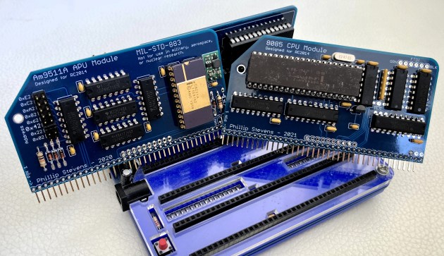
Intel 8231A APU + Intel 8085 CPU

Intel 8231A APU Module with Intel 8085AH-2 CPU Module

Perhaps the culmination of the path was building an Intel 8085 CPU Module for the RC2014 platform, and then adding an Intel 8231A equipped APU Module to the solution, together with the 8085 drivers for the z88dk am9511 maths library which makes, in my opinion, perhaps the perfect 1970’s computing machine.

4x APU Modules with Am9511A

4x Am9511A APU Modules with Z80 CPU.

What is even more perfect is that the APU Module can be scaled for efficient parallel processing, something that would never have been contemplated back in the 1970’s.

Yet Another Z180 Project (YAZ180)

I’m thinking about a new project, something a little unusual but still with a rich history of information upon which to base the build. On Tindie, I found the RC2014 project which is a build of a Z80 platform but based on some modern components. That got me thinking. My next project must be a Z80 based project.

Why the Z80? Well, it was at one stage the most used CPU in the world, which leads to the great depth of information and experience available for designs, hardware, and software. Technically, it is advanced enough to avoid the need for a large number of ancillary chips, multiple power supplies, and multi-phase clocking that the 80088080, and other older chips needed, but still it is complex enough that in doing a project I’ll feel like I’m actually building a computer.

This year marks 40 years (yes 40 years, since launch in July 1976) of the Z80, and still as a design and platform it looks like it will continue to be relevant into the future. So rather than building yet-another-ARM project. It looks like I will be marking the 40th anniversary of the Z80 with a new build.
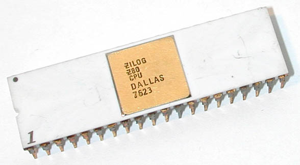
Zilog_Z80

An early Z80, manufactured in June 1976.

What kind of project? The RC2014 project is an interesting starting point. It is quite simple, being a compact and robust implementation of Grant Searle’s 6 Chip Z80 Computer, but provides more resources than most of the 1980’s Z80 projects offer. After looking at some projects others have done, I think that I should aim to build something a little like a “Back to the Future” Z80 project, a DeLorean (which also appeared as a prototype in 1976) with a fusion reactor.
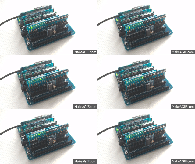
RC2014 Cylon

RC2014 Cylon

As an outcome I’d like the solution to be able to interact with modern interfaces such as I2C, Ethernet, SPI, and USB, with access to a large physical memory space, with great performance, and yet retain the ability to be a single-step-able experimental platform with LED bus indicators. Single stepping is something that you can’t do with an Arduino, and it is a real differentiation.

Whilst it would be attractive to design in some old-school interface devices, like the Am9511A APU or a Super I/O device, in light of today’s environment the wouldn’t contribute very much to the outcome. So the focus will be squarely on modern I/O.

Also, there is a temptation to build a CP/M system with full disk management. But again there are plenty of CP/M systems around. I’d like to build something more  of an embedded platform, that doesn’t require mass storage to run applications. It would be good if most of the basic interfaces could fit on one board, to avoid the need to build address and data bus extension. I think this will simplify the design significantly.

Design process

This is going to be an iterative process. The first step will be to build the RC2014 project, and test that I can program it.

It will be important to learn a little about Z80 assembler. Later, I may modify the RC2014 project platform.

Then, I’ll lay out a through hole prototype with minimal functionality, to test some performance ideas. If they work on through hole, then they’ll work with SMD. Using through hole also allows me to quickly fix logic or wiring errors that would take a new spin with SMD.

Finally, I’ll build a SMD device that miniaturizes the solution, and makes it more robust.

Processor selection

The Z80 has been built continuously for 40 years, and in that time many manufacturers have produced silicon and several clones have been created. The Z80 range been continuously improved through the Hitachi 64180, to the Zilog Z180, and the Zilog Aclaim eZ80 devices. Each increment has integrated more accessory components, and improved the instruction throughput, as well as increased the clock rate.

Looking at the options available, the original Z80 requires logic to get started. So rather than building serial ports and timers, it looks like the Z180 might be the right place to start. So why not go all the way to the eZ80? Well the eZ80 is not dissimilar to an AVR ATmega device, with all of the system components integrated into the one device. Using an eZ80 CPU wouldn’t be like building a computer at all. It would be much more like building an Arduino, and I’ve been there already.

Out of the Z180 options, I would select the Z8S180 (at 33MHz) because it integrates sufficient material to get started (Timers, Interrupts, MMU, & USARTs), and leaves me the option to add complexity as I get going.

Memory selection

A little research on the processor and available memory provides me with some cornerstones for the design. I will use Flash memory for the  program storage, and static RAM for the system memory. Historically, UV erasable PROM and dynamic RAM would have been used. One advantage of static RAM is that the solution is fully single-step-able. Meaning, I’ll be able to watch the address bus and data bus process each instruction as the Program Counter marches along.

The Z180 can address up to 1MB of physical address space, and it makes sense to provide the full physical memory possible. The price of 1MB of SRAM or of 256kB of Flash is almost nothing these days. As the Z80 logical address space is only 64kB, the Z180 has an inbuilt MMU to manage its physical memory to logical memory mapping.

Memory mapping

NOTE 2017 October: The details in the below discussion are no longer accurate. The memory design has moved on substantially, but this discussion remains for information only. Happily, even completely changing the memory mapping can be done with a software reconfiguration of the Memory / IO logic device.

To keep things simple (in hardware), we can use the MMU available in the Z180 to map the physical memory locations on 20 address lines, into logical addresses that suit us. The MMU can map 4kB pages of physical memory into two relocatable logical locations in the Z80 logical address space. These are called the Banked and the Common 1 locations. The Common 0 memory location begins at physical address 0x00000, and continues to the beginning of Banked memory, which then continues to the Common 1 memory address space.

Therefore the hardware (or physical mapping) will show that the 256kB Flash is located from 0x00000 to 0x3FFFF, and the 1MB RAM from 0x00000 to 0xFFFFF but the lower quarter of the RAM address space mostly masked by Flash. For programming we’ll have to move this around.

When the Z80 starts up it always begins from physical and logical address 0x0000. Therefore it is typical to put the program storage in the lower address range, and the RAM in the upper range. Given the use of the MMU available in the Z180 we initially can map the SRAM into the upper 32kB of logical address space, using the Common 1 bank and CBAR setting, leaving the first 32kB of Flash in the lower address range.

One difficulty is that there are only 3 memory spaces available, so if we want to have a C stack, global buffers and queues, and global data, then we need to put some SRAM in the Common 0 address space. Let’s uncover 8kB of 1MB SRAM and place this from 0x2000 to 0x3fff to provide this C stack and global variable data frame.

At some stage I assume I’ll want to use all of the additional Flash and SRAM available, so I’ll have to integrate programming for MMU bank switching, and RAM heap/stack switching when the need arises. At least initially there will be a statically programmable range of between 8kB Flash with 56kB SRAM to 56kB Flash with 8kB SRAM available within the logical address space, depending on the MMU initialisation settings.

To program the Z180 with a soft programmer, the physical memory addresses will need to be juggled around (glue logic) to disable the Flash and SRAM from appearing in the first 8kB Bytes of the address space. The USB soft programmer will provide program codes in the form of a remote boot-loader to load the contents of programs into the Flash, by moving the entire physical flash through a 4kB or 8kB Banked page. SRAM located in the lower 32kB address range will be loaded with a program to enable buffering and page writing of the desired programs.

Physical Address Range Run Mode Programming Mode
$00000 – $01FFF Flash (8,192B of 256kB) USB (8,192B)
$02000 – $03FFF SRAM (8,192B of 1MB) SRAM (516,096B of 1MB)
$04000 – $3FFFF Flash (245,760B of 256kB)
$40000 – $7FFFF  SRAM (768kB of 1MB)
$80000 – $BFFFF Flash (256kB of 256kB)
$C0000 – $FFFFF SRAM (256kB of 1MB)
Logical Address Range Run Mode Programming Mode
$0000 – $1FFF Flash (8,192B, Common 0) USB (8,192B)
$2000 – $3FFF SRAM (8,192B, Common 0) SRAM (24,576B, Common 0)
$4000 – $5FFF Flash (8,192B, Common 0)
$6000 – $7FFF Flash (8,192B, Banked)
$8000 – $FFFF SRAM (32,768B, Common 1) Flash (32,768B, Banked)

The programming mode (address mapping) will be entered by either a button press, or by signalling from the USB – USART interface lines. The process is to invert the Address 19 line, shifting the physical address location of Flash, and mute Address 0-12 to prevent memory being read from these locations, which allows the USB – USART FIFO to provide program opcodes. Mute by disabling the CE on both Flash and SRAM when A13 through A19 are 0. Then configure the MMU to bring the Flash into Banked logical addresses, using the SRAM to buffer 4kB page writes to Flash memory.

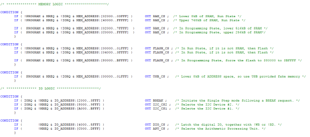
Using the ATMEL WinCUPL tool, it is pretty straightforward to convert the above memory mapping and below logic mapping in CUPL language description to JEDEC format that can be handled by a MiniPro TL866 EEPROM & PLD Programming tool, and programmed into an ATF16V8C  or Lattice GAL16V8D device.

MEMORY_PLD_A

CUPL Memory / IO Definitions

MEMORY_PLD_B

CUPL Memory / IO Decoding

This memory and IO mapping needs to be augmented by a secondary logic mapping for managing programming, single step, and other functions, which will be programmed into a second ATF16V8C or GAL16V8D device. The logic mapping will allow automatic programming initiation via the FT245R USB interface.
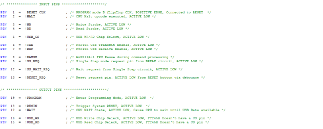
LOGIC_PLD_A

CUPL Logic Definitions

LOGIC_PLD_B

CUPL Logic Decoding

Using EEPLD devices will save significant PCB real estate, and will allow me to compensate for minor logic errors after the fact.

screenshot-from-2017-01-28-20-06-10

Schematic for Memory GAL

yaz180-logic-schematic

Schematic for Logic GAL

FCPU selection

The best Flash memory we can get easily is 55ns timing. This is bettered by SRAM, with 45ns access timing. By converting this timing to a bus frequency we can achieve 20MHz or slightly better, but allowing for some buffering or address logic delay it would be better to keep the system bus under the equivalent of 20MHz.

Using this system bus speed of approximately 20MHz then poses a question; which is the right speed? Some references point out that the Z180 is very poor at holding the correct USART rate when the CPU clock is not a magic multiple of the USART rate. This is the same issue that the AVR ATmega device faces when its USART is not driven by a magic frequency clock. Therefore, lets us set  the CPU crystal oscillator to 18.432MHz, being most appropriate magic frequency for the following design.

The Z180 system clock (or PHI) can be double, equivalent, or half the rate of the crystal oscillator base rate. Starting with 18.432MHZ oscillator clock, depending on the CPU Control Register (CCR), the system bus clock (PHI) can be halved and is operated at 9.216MHz. This is slow enough to allow most peripherals to interact with the CPU. Internally, the system bus clock (PHI) can be doubled to operate the CPU at 36.864MHz, by setting both the Clock Multiplier Register (CMR) and the CCR. This rate is slightly overclocking the Z180, but that’s what we live for. We don’t build slow computers.

As we are using 45ns SRAM and 55ns Flash, we will have to insert either 1 or 2 memory wait states when operating at 36.864MHz. This is unavoidable, because of the access speed of both memory devices. Faster SRAM may be available, but faster Flash is quite hard to obtain.

I/O Mapping

I have been thinking about the whole idea of system modularity. Actually, I don’t think the traditional method of building a backplane is such a good idea for what I want to achieve. Extending the address bus a long distance means that I’ll be investing in design and timing issues, that I’m not really sure I know how to solve. So, let’s focus on a smaller design, with on just one board for the time being.

As a computer always needs to be extended and interact with the real world, I think it would be good to add modern user interfaces to the solution. Use Address 15-13 to provide I/O selection options on the CPU Board, using the remaining output pins from the Memory ATF16V8C or GAL16V8D. This will allow flexibility to latch data into the Hex Display, or trigger breakpoints using #M1 and #Wait to allow Single Step execution from any code point.

I/O Address Range Chip Select (A15,A14,A13) Device
$0000 – $1FFF DO NOT USE ($0, b000) Internal I/O
A7-A0
Internal INT
$0000 – $00FF Registers
$2000 – $3FFF BREAK ($1, b001) Break Point Toggle Single Step Mode
$4000 – $5FFF #DIO_CS ($2, b010) PIO 82C55
A1-A0
$4000 – $4003 Registers
$6000 – $7FFF EXPANSION ($3, b011) Hold for Expansion
$8000 – $9FFF #I2C_CS2 ($4, b100) PCA9665
A1-A0
#INT2
$8000 – $8003 Registers
$A000 – $BFFF #I2C_CS1 ($5, b101) PCA9665
A1-A0
#INT1
$A000 – $A003 Registers
$C000 – $DFFF #APU_CS ($6, b110) APU_CS – Am9511A-1
A0 & #WAIT
#INT0
$C000 – $C001 Registers
$E000 – $FFFF EXPANSION ($7, b111) Hold for Expansion

Included I/O features & BOM

CPU

SRAM

Flash

Single Step – The Z-80’s #M1 pin is useful for building logic to single-instruction step the machine. You do this using the memory ready signal on #M1 to clear a 7474 flip-flop, which is clocked by a Single Step signal, to produce a #WAIT signal for the CPU. That stops the machine on the opcode fetch cycle with the address showing on the address bus and the opcode byte showing on the data bus. To move the machine ahead, you clock the flip-flop which releases the #WAIT signal, until the next #M1 clears the 7474  again.

Reset

Memory & Addressing Logic Glue

  • Programmable Logic PLD – Digikey ATF16V8B

USB – Flash programming interface

  • USB-Parallel Bus FTDI245RQ
    Note that  the Write strobe is confusing, but assume ACTIVE LOW.

USB – USART interface

  • USB-Serial FTDI232RQ

Hex 7 Segment Display – 5x Address Digits – 2x Data Digits

  • Decoder DM9368 – Digikey DM9368N-ND
  • LED Display VDMY10C0 & VDMG10C0 – Digikey VDMY10C0TR-ND
  • OR
  • LED Display with Decoder TIL311A – eBay only.

General Digital Input / Output – Being able to read and write simple digital levels is an important thing. So let’s include the 82c55 PIO device.

  • Intel CMOS 82C55 Programmable IO CP82C55A – Digikey CS82C55AZ-ND

I2C interface – This is the most important interface, which provides many extension options, and a plethora of Grove System sensors. Unfortunately the 5V nature of the system precludes using the newest really fast, deep buffer, devices with multiple bus I2C 1MHz bus interfaces, so provide 2x devices to support different applications (eg. video output and sensor acquisition on separate buses). Use the #INT1 & #INT2 interrupts.

Arithmetic Processor Unit – This lovely old chip is now also 40 years old, and was the world’s first APU (or FPU). Potentially, it is too slow to contribute, but still we’ll build it in. Need to provide a 3MHz clock to drive it (FAPU = FCPU/6), and connect its #PAUSE to #WAIT. #END connected to #INT0. RESET is ACTIVE HIGH.
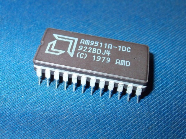
AM9511A-1DC

Am9551A-1 3MHz APU

Bus interface

  • Address & Control – Octal Buffer Driver sn74abt541b – Digikey 296-14668-1-ND
  • Data – Octal Bus Transceiver sn74abth245 – Digikey 296-4140-1-ND

Power Supplies

Excluded I/O features & BOM

Ethernet – Wiznet W5300 Direct address mode requires 3FF of address space. Configure the #INT0 interrupt and implement the DMAC1 I/O to move packets quickly. Exclude this from the initial build, as it is quite a complicated 100 pin device, and it needs 3.3V supply.

USB & SPI interface – provide mass storage capability using either USB or SPI interface devices. The CH37x series is not very well documented, or readily available. There are other options for I2C-SPI bridging which can provide an SPI interface if needed.

  • CH376S – Incorporating the USB functions as described in CH375, and CH372

ADC interface – Better, higher resolution, faster chips are available with I2C interfaces.

  • 8 bit ADC with internal reference MAX158 – Digikey MAX158ACPI+-ND

Video Interface – Can be done using an external I2C device.

  • LCD Video – via I2C with a FTDI EVE

Super I/O – Floppy Disk & IDE Controller – Too hard and doesn’t bring much value to the table. Floppy drives are hard to find, and there are already 2x USART ports available on the Z8S180.

Software & References

Z80 Info

z88dk Development Kit

Small Device C Compiler

SASM Softools – Z180 (MMU aware) C compiler. Commercial Licence.

Programming the Z80 by Rodnay Zaks

The Undocumented Z80

Logic Families

FreeRTOS 9.0.0 for eZ80

Hardware Design notes

Well quite a few iterations on my aspirations and thoughts have resulted in a YAZ180_v1 schematic, that I think is now basically frozen. Some of my design decisions follow.

After deciding not to use the TIL311 LED display devices because they are not easily obtainable, I found the alternative solution using the DM9368 display driver chip and LED display devices was very consuming of space on the board. Since the board had to be no greater than a maximum of 10cm by 16cm to fit within the constraints of my Eagle Hobby licence, I decided to buy some TIL311 devices in advance, and then with the comfort of stock in hand I could use them for the design. Also, they add significantly to the retro-chique.

I would have loved to add the Wiznet W5300 device to the design to provide high speed Ethernet capability, but with a 100 pin VLSI it was just too complicated for the initial design. Next time.

I added a 82c55 interface chip. Knowing that it is very slow, requiring 2 wait states to drive it, is one thing. But the advantage of having multiple latch-able input and output ports, off one fairly compact integrated device made up for that problem. As it is a 1970s device it is also retro-chique accretive.

Designing using CUPL and the Atmel or Lattice PLDs is in my opinion much simpler than tracing schematics and thinking through 7400 series NOR, NAND gates to get the desired addressing logic. Writing the logic in “c” like syntax is much less taxing on the brain.

After deciding to implement no bus drivers, and then building a solution adding drivers and termination to every address and data line, I have rationalised down to bus drivers on data, lower address, and control lines. These are the few lines that appear on all memory and I/O devices, and are taken to every point on the board. The upper address lines only appear on the PLD, SRAM, and Flash, which are very low load modern devices, so there is no point to buffer them. Using ABT logic limits the differential delay on the address lines to 2 ns, and since the read and write select lines are also buffered, there is no issue timing issue created.

And here is the first schematic, in pdf YAZ180_V1. Errors and omissions did occur.

Hardware Layout notes

With the first major layout session behind me, I have the following notes.
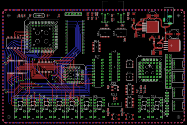
Address&DataRouted

Address & Data to SRAM and FLASH

Change the SN74ABT244 for the SN74ABT541. The only difference is the pin ordering, with the 244 being optimal for counter-flowing signals, and the 541 being optimal for unidirectional signals (physically). This will help layout.

Getting 20 address lines and 8 data lines to appear on the SMD SRAM memory is challenging. I will probably reassign the address lines to suit the Z8S180 pin-out, rather than spending hours untangling the lines. It won’t be too easy to do this with the Flash device, but as it is in a PLCC through-hole socket it comes inherently with “vias” making reaching it half as hard as SMD.

Input pin and I/O pins on Z8S180 include weak latch circuits to prevent excessive current draw by the receiver, if the pin is not externally driven. External pull-up or pull-down resistors should not be less than 15 kOhms to ensure that the resistors can control the state of the latch when power is supplied.
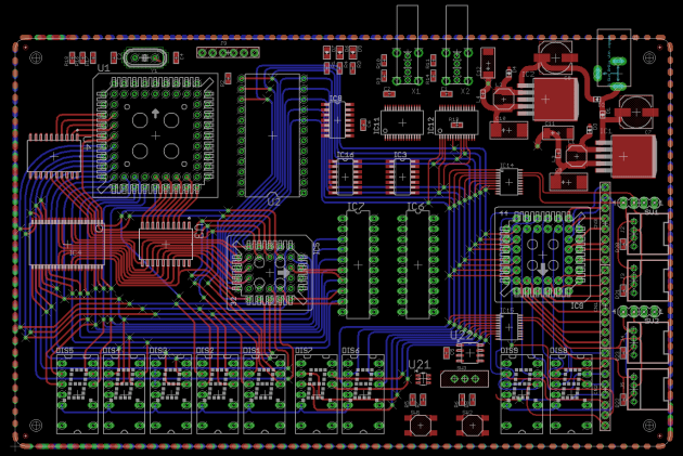
Address&Data

All Address and Data lines routed.

afewmoreairwires

A few more air-wires remain, that will need thought.

Following about 10 hours of juggling, just two wires remain together with a plan to resolve them tomorrow.
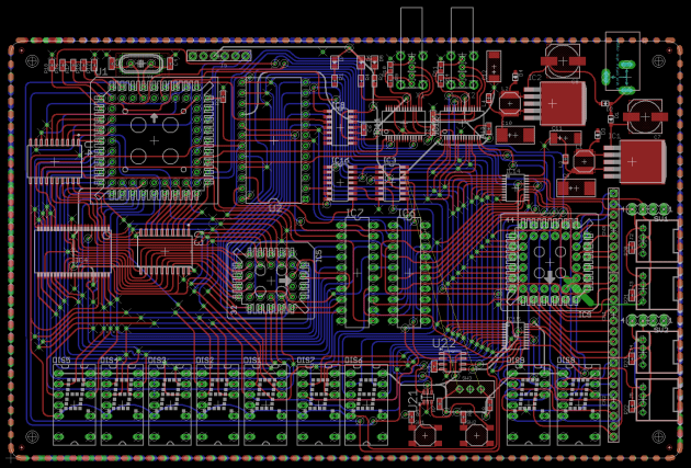
twoairwires

Just two air-wires remain.

Finished, except for the detailed checking, which usually results in some changes. But, it is done.

The screen grabs below show with the Vcc Layer in Grey, and GND Layer in Green. I have added some basic traces on those layers to close off the routing, which are misleading. The layers are actually completely filled, normally.

This slideshow requires JavaScript.

Bill of Materials

Well, building this retro-computing machine is not quite as cheap as an ATMEL micro-controller board. But then again, it is not quite in the same league, with 1MB of RAM, and 256kB of Flash storage, together with an APU and 9 digits of LED display.

I have ordered all of the components, except the Am9511A-1 APU and the TIL311 LED display devices, from Digikey. The BOM is detailed in this link. To add to BOM, this there are the Am9511A-1 and the TIL311 devices which can be found on eBay or other auction sites.
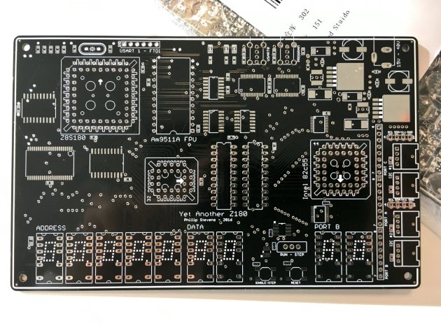
CoL3S3MUkAAksZ5

And, the PCB looks great!

Bringing up the Prototype

The build and bringing up of the board will continue, once I get the new SMD oven sorted out.

Well, the board has been soldered, and everything looks good. The SMD oven wasn’t as useful as I thought. It turns out that I can solder the fine pitch of the SRAM and FTDI devices fairly well with a normal soldering iron.

My PLD programmer won’t work with ATMEL devices, so I’ve been waiting so long for some Lattice GAL devices to be shipped to me. Over 8 weeks in transit. Finally they’ve landed. So I soldered the rest of the board together.

I’ll have to debug my CUPL programming of the GALs to get everything working, but at least there’s no “magic smoke”.

The TIL311 LEDs are very hot, because they draw so much current. LEDs really have come a long way in efficiency over the past 30 years.

Update 9 Jan 2017. Using this Github Repo, I’ve successfully sent characters to the ASCI. It lives!

Update Friday, January 13th 2017. Initial RAM testing passed!

And now based on this testing, I’ve been able to get the ASCI0 (and ASCI1) working, so that I have NASCOM BASIC Ver 4.7 (1978) running on my 2016 designed computer!

This is a Mandelbrot program running in NASCOM Basic v4.7.
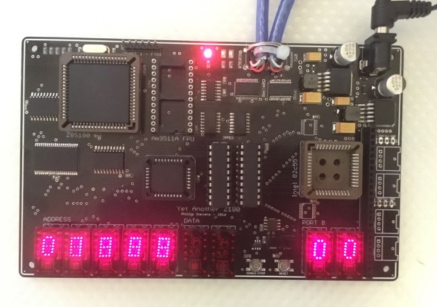
yaz180-glow

Glowing, in a dark  room.

Three major items remain to complete, before a PCB revision.
  • Completing the “in circuit programming” tools, to programme the Flash memory without removing it.
  • Writing drivers for the Intel 82C55 PIO device.
  • Writing drivers for the AMD Am9511A APU device.
Following the PCB revision, I’ll work on the I2C platform, and its drivers.

Next up, programming Flash memory using the FTDI FT245 USB-Parallel port. This was working, but some bad soldering made the on-board FT245 inoperable. Testing was completed using an external device.

Testing for the 82C55 PIO device is now done. It can do a lot more than this, but the proof of life is completed. Time to move on.

Update February 20, 2017. Despite initial misgivings, that the Am9511A APU was wired incorrectly, the proof of life for the APU is now done.

For a long time, I could see that the APU was trying, but just wasn’t making it. Two issues were involved.

Firstly, all of the datasheets assume 74 logic is being used to create the chip select from 3 to 8 address decoding, or similar solutions. What they don’t point out is that the Am9511A  APU chip select MUST be generated from the address lines, because the Z80 (Z180) IORQ line has incorrect timing to drive the Am9511A. The Am9511A needs an 30ns of chip select and address validity after WR is raised, which the Z80 IORQ timing doesn’t provide. Having infinite logic in a GAL available, I had (incorrectly) included the IORQ line in the APU_CS logic. Whilst I’d recognised the issue, it took three lines in an obscure 1981 PhD dissertation to focus the spotlight of clarity. Thank you Mr Haining.

Secondly, the Am9511A samples I have on hand won’t work at 3.072MHz. I guess they were cutting very close to the limit in the day.
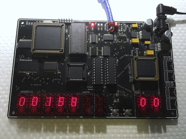
img_0626

YAZ180 v1 full configuration.

I’ve finished an initial revision of the PCB to fix all of the known errata. I’ll sit on it a bit until I can double check that everything is good.

Errata

The power supply section was done very simply in the V1 build. I underestimated the requirement for 5V power, thinking that 1A should be sufficient. Before I built the V1 board I realised my error and replaced the 5V 1A regulator with a AP1506 that can supply 3A. I also changed the inductor to a lower inductance and higher current version.

I’ve now revised the power supply  section to use LM2596 3A device for the 5V supply, as this device has a larger input voltage range (up to 40V) , and I have inserted thermal vias to improve the heat spreading into the back side of the board.

The 12V supply only needs to provide about 90mA for the APU. I’ve reduced the capacity of the regulator down to 500mA, and have saved some space by using a LM2674 in SOIC-8 format. Whilst the Am9511A gets uncomfortably warm, the power supply doesn’t.

Also, I simply forgot to provide a 3.3V supply, that is required for the I2C interface devices. So this has been repaired with a 1117 linear regulator, supplied by the 5V regulator. It is the same device I used in the Goldilocks Analogue as I have some parts in hand.

I’ve swapped the USB connectors to male versions. Can’t understand why I built YAZ180 V1 with female connectors. Just silly.

I’ve swapped the location of the RESET and SINGLE_STEP buttons. It makes more sense to have the buttons doing the same function closer together.

The Z8S180 requires that its DCD0 be held low, before the USART0 can transmit. This pin is now tied to GND.

The Logic GAL device, in Registered Mode, requires to have its OE held low. This pin is now tied to GND.

To generate a RESET signal, the reset request input to the Logic GAL can’t be on Pin1 in Registered Mode, so the RESET_REQ signal was moved to Pin14. Pin1 in Registered Mode is connected exclusively to the CLK for the GAL flip-flops. In order to clock the flip-flop implemented in the YAZ180 programming mode logic, the RESET line was connected to Pin1.

The Am9511A-1 although specified at 3MHz, doesn’t pass tests at 3.072MHz. So it will have to be de-rated to 1:8 from the Z8S180 system clock. This takes the clock speed down to 2.304MHz. The clock divider chip will be replaced by a sn74ls93 from Digikey 296-3749-5-ND.

For the purposes of enjoyment, I’ve connected the Z8S180 DMA engine DREQ1 and TEND1 lines to the Am9511A SVREQ and SVACK lines. The SVREQ requires a NOT to generate the inverted Z8S180 signal for DREQ1. Although there are very few bytes loaded into the Am9511A, this should allow them to be written by the DMA engine.

Both AMD Am9511A and Intel 82C55 need the address and chip select lines to remain valid for a period after the RD or WR signal has gone high. Therefore we need to remove the existence of a valid IORQ signal from the calculation of their select line, and just rely purely on their address decoding (and absence of MREQ). The CUPL coding has been adjusted

The Am9511A supports 1 I/O Wait State, as RD & WR to Pause is 100ns. The 82C55 requires 2 I/O Wait states, as RD is 200ns minimum.

Update February 24th.

The new PCB has been ordered.

I’ll start a new post for the YAZ180 V2 when the PCB is back from manufacturing.