There has been quite bit of interest in assembly or machine monitors for the RC2014 lately, so I’ve taken the opportunity to write one in MS (NASCOM) BASIC which will work for RC2014 Mini / Micro / Classic ][ machines, but equally well for any machine running a version of MS Basic 4.7 or later.
The functional goal was to provide the same user tools as the NASBUG monitor, but to be maintainable and easily customisable by the user. As the monitor is written in BASIC it works equally well for both Z80 based RC2014 machines and 8085 based RC2014 machines using my 8085 CPU Module (for example).
A key issue for me was that it needed to fit completely into the BASIC program memory found below the default z88dk assembly loading address of 0x9000 for the RC2014 target.
By using BASIC language for the monitor it enabled me to focus on the functionality, as BASIC provided the command line support via INPUT(), string tokenisation via MID$(), ASC(), and VAL(), and mathematical functions.
However, Fred W. has provided a better simpler solution for getting an integer from a hexadecimal string and now that solution has been implemented.
With that key function done, then the MID$() function was used to tokenise the command string into 4 (or less) digit strings to convert into hexadecimal. Depending on the function required either signed integers were then produced to be an address or where a length was needed an unsigned integer was provided.
Finally an IF THEN tree was made to process the command string, found using the very convenient ASC() function. Since the commands are sparse, I thought that a simple decision tree would be best.
As noted, a key goal for me was that it needed to fit completely into the BASIC program memory found below the default assembly loading address 0x9000. The program fits with over 100 Bytes free, currently. But the stripped version has still over 1200 Bytes free, so there is quite a lot more code that could be added if needed.
Program Usage
The BASIC monitor is useful to casually poke around in the RAM or ROM of a running MS BASIC RC2014 machine to get a feeling of how variables and strings are stored, for example.
It can be used to enter assembled binary code into the RAM, and then run it. The assembly code can use the facilities (serial I/O, RST table, and MS Basic functions) as needed. Some further information on Assembly can be found here.
Further, it can be used together with the Zen Editor/Assembler to write and then assemble larger programs for the RC2014. When the monitor is used together with Zen, the monitor can be loaded (copy / pasted) into the BASIC Command Line, then using the BASIC HLOAD command Zen can be loaded (cat) into the RAM at 0x9000, and launched either from the monitor or directly using ?USR(0). Once editing and assembly is finished, Zen can be exited with Q and then the newly assembled program can be run from its origin by entering the monitor with run, and then E xxxx yy, where yy is a signed integer input parameter.
Using this combination of Zen and the BASIC monitor it is possible to develop, examine, and modify complex Z80 and 8085 assembly code in a very comfortable environment.
Commands for a BASIC Monitor (Syntax borrowed from NASBUG)
A – hexadecimal arithmetic
A xxxx yyyy – Responds with: SSSS DDDD JR JJ. SSSS is sum of xxxx and yyyy. Values in Hexadecimal. DDDD is difference of xxxx and yyyy, yyyy-xxxx. Values in Hexadecimal. JJ is displacement required in a Jump Relative instruction which starts at xxxx, to cause a jump to yyyy. Value in Decimal.
C – copy
C xxxx yyyy zzzz Copy a block of length zzzz from xxxx to yyyy. One byte is copied at a time, starting with the first byte, so if there is an overlap in the two areas data may be destroyed. This command is useful for filling a block with a single value. Make yyyy one greater than xxxx and put the required value into address xxxx using M. Set zzzz to the number of bytes required. Values in Hexadecimal.
E – execute
E xxxx yy – Execute program at xxxx, supplying integer input parameter yy. The USRLOC location depends on the specific MS BASIC ROM implemented. The value can be easily adjusted in the monitor source code. Values in Hexadecimal.
I – intelligent copy
I xxxx yyyy zzzz – Like the Copy command but copies to ensure it will not cause data corruption in an overlapping section. Values in Hexadecimal.
M – modify store
M xxxx – Modify memory starting at address xxxx. The address is displayed followed by the current data. The data value may then be changed. Continuous entry of new data values is supported. Values in Hexadecimal.
Q – quit
Q – Quit to BASIC Immediate Mode (Command Line).
T – tabulate
T xxxx yy – Tabulate (display) a block of memory starting at xxxx and continuing to yy-1. Values in Hexadecimal.
Further Development
As the monitor is written in BASIC it is easy to maintain for all hardware or CPU types wherever MS BASIC is found, and to further develop to support new functions. As there are about 1200 Bytes free below the default origin (in the stripped version), there is space for the user to add their own preferred functions or modifications to existing functions.
Just over 4 years ago, on 18th March 2018, I committed the first CP/M-IDE files into the RC2014 repository. Now that some time has passed and it has developed into a stable solution for CP/M I think it is time to fill in some details about why it was written, how it differs from other CP/M implementations, and how to reproduce images to match those in the CP/M-IDE repository.
Concept
There are several implementations of CP/M available for the RC2014. Initially, the CP/M on a Breadboard project implemented by Grant Searle became the default implementation for the Z80 RC2014. Slightly later Wayne Warthen added support for the RC2014 to the Z80/Z180 RomWBW System. RomWBW is a very extensive and advanced set of system software, supporting many different RetroBrew machines, and in general it requires 512kB ROM and 512kB RAM to reach its full potential.
Each of these implementations has its own focus. The 9 Chip CP/M is based on simplicity, and being able to be built on a breadboard with the minimum of complexity, but it has not been maintained (e.g. correcting the bugs in the SIO and ACIA serial implementations requiring arbitrary interstitial delays to be inserted, otherwise data loss occurs) and it has a substantially smaller TPA. Alternatively, RomWBW supports a variety of hardware including Z180 CPUs, and provides an underlying generalised architecture support which provides paged memory and many facilities but this imposes a processing overhead on I/O, and requires substantially more RAM (512kB) than a typical CP/M system.
Faced with both these options, and being very interested to build my own solution, and to use my growing experiences supporting the z88dk community, I decided to build CP/M-IDE to fulfil a specific niche.
The CP/M-IDE is designed to provide support for CP/M on Z80 while using a normal FATFS formatted PATA or IDE drive. And further, to do so with the minimum of cards, complexity, and expense. Most recently, it has also become the CP/M which supports the 8085 CPU Module. Also recently, support for the standard RC2014 Pro with CF Module v2.1 and for the RC2014 Mini II with CP/M Expansion Kit has been added.
Initially I chose the IDE Hard Drive Module specifically because I could use it to attach any old hard drive, aka “spinning rust”, to my RC2014, and this led to support for everything from these old 3 1/2″ hard drives, through to modern SSD or DOM solid state drives. It also supports both old and modern high capacity Compact Flash Cards in their native 16-bit mode, so readily available modern 1 and 2 GigaByte Compact Flash cards are OK. It is also possible to use SD Card to CF Card adapters with the IDE Hard Drive Module or the CF Module v2.1, allowing direct support of modern pluggable SD or Micro SD storage.
I also wanted to build a very inexpensive system so the original RC2014 Pro with CF Module v2.0, or RC2014 Mini with CP/M Expansion Kit, is sufficient for modern storage solutions. And as an option the RC2014 IDE Hard Drive Module is the only additional Module required to operate CP/M-IDE with older “spinning rust” hard drives. It is NOT necessary to buy an expensive 512kB/512kB Memory Module as the standard 64kB RAM Memory Module works fine. If there’s no need or interest to attach proper IDE hard drives, or using a Compact Flash Module for storing CP/M drives is preferred, then there is no additional hardware required over the RC2014 Pro standard product.
CP/M is a very compact Operating System and, in the most common version 2.2, it supports only serial interfaces and disk interfaces. For the RC2014 there are two standard serial Modules, being the ACIA Module (used in the RC2014 Mini) and the more advanced and expensive SIO/2 Module (used in the RC2014 Pro).
As I’m quite interested in building real-time and event driven systems, in contrast to other CP/M implementations, CP/M-IDE therefore includes drivers supporting both transmit and receive interrupt based solutions, sourced from my z88dk RC2014 support package for the ACIA serial interface and the SIO/2 serial interface.
8085 CPU Module
More recently I have built a 8085 CPU Module for the RC2014 System. This is the first time that an 8085 CPU has been integrated into the RC2014 System, and it is able to work with the Z80 bus signalling required to drive the standard RC2014 Modules.
CP/M-IDE 8085 RC2014 System
I am very pleased to have a wholly Intel RC2014 System equipped with the 8085 CPU Module, the 8231A APU Module, and the 8255 IDE Module. This is the original “Intel Inside”, before it became marketing jargon.
Hardware
The concept remains to use the minimum of additional hardware over the entry level RC2014 Pro model. In fact just the IDE Hard Drive Module is desirable. But, the standard CF Module v2.0 (and derivatives) can also be used as it supports modern (large capacity) CF Cards, and the RC2014 Classic II with CP/M Expansion Kit is also supported.
IDE Hard Drive Interface
The IDE Hard Drive Module is based on the 8255 PPI device. This device was designed to work with the 8085 CPU and 8086 CPU. It is perfectly suited to supporting a 16-bit parallel IDE interface as it provides latching of signals on 3 separate 8-bit ports.
Initially I was concerned that the selection of control signal pins for the IDE interface limited the possibility for use of the 82C55 device for generalised I/O. I still think that this is an issue but, since no one has implemented further generalised solutions, the point is moot.
The IDE Hard Drive Module supports PATA hard drives of all types (including SSD IDE and DOM storage) and Compact Flash Cards and SD Card Adapters in native 16-bit PATA mode with buffered I/O being provided by the 82C55 device.
The IDE interface (or also termed diskio) is optimised for performance and can achieve over 110kB/s throughput using the FatFS library in C. It does this by minimising error management and streamlining read and write routines. The assumption is that modern IDE drives have their own error management and if there are errors from the IDE interface, then there are bigger issues at stake.
The CF Module interface can achieve over 200kB/s throughput at FATFS level, and seems to provide best performance using SD Cards in SD Card to CF Card Adapters. The old default RC2014 CF Module v1.3 is often unstable with modern CF Cards or with SD to CF Card Adapters. However the recent RC2014 CF Module v2.1 has become quite reliable with all modern large and small CF Cards. If you experience problems, then seek out this recent implementation.
For both IDE interfaces, within CP/M performance is approximately half the FATFS performance because the CP/M deblocking algorithm implements a double buffer copy process where 512 Byte physical sectors found on IDE disks are converted into the 128 Byte logical disk blocks that CP/M expects.
Serial Interfaces
In the ACIA builds, the receive interface has a 255 byte software buffer, together with an optimised buffer management supporting the 68C50 ACIA receive double buffer. The choice of memory size for the receive buffer is based on optimisations available by having the buffer a full “page”. Also text can be “pasted” in fairly large chunks into the CP/M command line without losing bytes.
Hardware (RTS) flow control of the ACIA is provided. The ACIA transmit interface is also buffered, with direct cut-through when the 31 byte software buffer is empty, to ensure that the CPU is not held in wait state during serial transmission. The size of the transmit interface buffer is based on free memory within the CP/M BIOS. As BIOS memory is typically reserved to start on the 256 Byte page boundary, if an update needed to consume more RAM, I would reduce the size of the transmit buffer to avoid the need to consume an additional page of BIOS memory.
In the SIO/2 build, both ports are enabled. Both ports have a 127 byte software receive buffer supporting the SIO/2 receive quad hardware buffer, and a 15 byte software transmit buffer. The transmit function has direct cut-through when the software buffer is empty. Hardware (RTS) flow control of the SIO/2 is provided. Full IM2 interrupt vector steering is implemented.
As both ACIA and SIO/2 devices have a hardware buffer for received bytes, it is important for the receiving interrupt handler to drain these buffers completely before returning execution to the program. If this is not done there is a danger that received bytes could be overrun and lost.
For the CP/M-IDE 8085 build the Serial Output (SOD) FTDI interface found on the 8085 CPU Module is enabled as the CP/M LPT: interface. This is activated by using ^p as per normal practice.
Additional Hardware
Whilst there is no support for additional hardware within CP/M itself (as there are no BDOS calls standardised), it is possible to use additional hardware in CP/M applications. Typical hardware options include the APU Module, various Sound Modules, and digital I/O Module.
CP/M Implementation
There are many descriptions of Digital Research CP/M, so I won’t go into detail. It is important to know that CP/M v2.2 was in its day the most widely deployed Operating System for small computers based on the 8080, 8085, and Z80 CPUs. Later versions of CP/M supported the 8086, and 68000 CPUs, as well as providing many more system functions than the CP/M v2.2.
Whilst there have been later versions of CP/M produced, to my knowledge, there were no widely available user applications produced which could not be run on CP/M v2.2. This broad compatibility is why CP/M v2.2 is important.
CP/M v2.2 is essentially just 4 pieces of code. The BIOS (Basic Input Output System) is provided to abstract the hardware devices from the operating system. Essentially there is a limited set of BIOS commands that the BDOS can call on. These BIOS commands are implemented specifically for the characteristics each machine, and in the early days of computing it was essential that a user knew how to write their own BIOS.
The second piece of code is the Page 0 of memory, which is written by the BIOS cold boot command on initialisation. The role of this Page 0 is to provide important addresses (for both BIOS and BDOS) and to set important status registers like the I/O Byte. The Page 0 is also used to manage the 8080, 8085, and Z80 CPU interrupt vectors, and to store the command line entered by the user when an application is initialised.
The CP/M BDOS is the middle layer of the Operating System. Application programs rely on BDOS system calls to support their requirements. Here the drives (A:, B:, through to maximally P:) are opened and closed, and disk sectors are written. The BDOS does its work by calling BIOS commands on behalf of the application that is currently loaded.
Often the BDOS is combined with the CCP (Console Command Processor) into one assembly language file because both of these components are constant and they are independent of the hardware. These two components are essentially the distribution of Digital Research CP/M which was sold to the user.
The CCP is the user interface for CP/M. It provides a very small number of integrated commands, like “directory list”, “erase”, “rename”, “type” or “exit”, but its main role is to load additional commands or applications called “Transient Programs” into RAM and execute them. Often, an application loaded into the Transient Program Area (TPA) RAM will overwrite the CCP in memory as it is normal for the CCP (and BDOS) to be reloaded once an application quits.
There are third-party alternatives available for both the CCP and BDOS, and as these are loaded each time the computer is restarted it is possible to replace the default versions by alternatives if desired. Specifically for CP/M-IDE, the DRI CCP can be replaced by Microshell SH (here), or both CCP and BDOS can be replaced by NZCOM also known as Z System without impacting the installed ROM system components.
CP/M Drives
CP/M was developed before there was a standard implemented for computer disk drives, and every system had its own peculiarities. In order to cope with this situation each BIOS had to be written to cover the possibilities, by completing a Disk Parameter Block. Each disk type needs its own DPB, which takes space in BIOS RAM, so it made sense for CP/M-IDE to be implemented with only one type of disk supported. Additionally each drive attached by the BIOS requires a substantial Allocation Vector RAM reservation. It needs to be said that providing for unused drives in CP/M substantially increases the BIOS size, and commensurately reduces the TPA RAM for user applications and in turn their working RAM. For comparison, CP/M-IDE has 3kB more TPA RAM available for user applications than the default RC2014 CP/M implementation.
A subtle but important advantage to using only one disk type is that every disk is orthogonal, and it can be located anywhere on the underlying physical disk (ie. starting at any LBA). Also, it does not matter into which CP/M drive A:, B:, C:, or D: a disk is mounted when booting. The CP/M “system disk” looks exactly like any other disk, and every CP/M disk file can be located anywhere on the FATFS parent drive.
Further, the CP/M-IDE CCP/BDOS/BIOS operating system binaries are loaded from ROM. This is not typical, as most CP/M BIOS implementations will load the CCP/BDOS/BIOS from the first sectors (or tracks) of the first attached physical drive, and will require the system disk to be located in specific sectors of the physical drive, and they also rely on a specific allocation of LBA addressed sectors (or slices) for all additional drives.
The CP/M-IDE system supports a maximum of 4 active drives of nominally 8 MByte each. The maximum possible size of any CP/M disk is 8 MByte, due to overflow of a 16-bit calculation within the BDOS. Further each CP/M disk can support up to 2048 files as a maximum. By setting the standard CP/M-IDE disk type to be maximised both in terms of size and number of supported files there is no question of the disk storage being too small. The only limitation introduced is that up to a maximum of 4 CP/M drives can be active at any one time, which leaves us with the maximum free TPA RAM.
The choice of 4 drives for CP/M-IDE was based on nominally having 1 drive for CP/M system utilities, 1 drive for application files, 1 drive for user data or source files, and 1 drive for temporary files. In practice I’ve found that working with 2 or 3 drives is the most common scenario, and often it makes sense to copy the few needed system utilities onto a working drive and work off that one drive.
CP/M-IDE is like having a 4 “floppy” drive machine (with 8MB floppy disks), and a library of up to thousands of floppy disks to choose from. Just insert the floppy disks you want to use when you want to use them. This interchangeable disk strategy is different to other RC2014 CP/M implementations that put everything into a maximum of 16 “hard” drives, at fixed LBA locations or slices, and leave them attached permanently.
It should be emphasised that a CP/M-IDE disk is purely a normal file from the perspective of an IDE FAT32 (or FAT16) formatted disk. It can be copied, moved, compressed (or zipped), or archived by any disk tools, in any modern O/S, as desired.
As CP/M-IDE uses LBA addressing there can be as many CP/M disks stored on the IDE FAT32 (or FAT16) formatted disk as desired, and CP/M-IDE can be started with any 4 of them in any drive. Note that CP/M does not know about or care about the FAT file system. On launch the CP/M-IDE BIOS is provided with an initialisation LBA for each of its 4 drives by the boot shell, and all future sector references to each disk (file) are calculated from these initial LBAs as provided for each drive.
As the FAT32 format supports over 65,000 files in the root directory, and a similar number of files in each sub-directory, collections of hundreds or even thousands of CP/M disk files can be stored in any number of sub-directories on the FAT32 parent disk. Knock yourself out by storing every conceivable CP/M application on thousands of disks on a single 120 GByte drive. As the CP/M Operating System doesn’t store state (the CCP/BDOS is reloaded each time an application terminates), changing or reordering drives is as simple as typing exit, and then restarting with the new drives desired using following shell command: cpm filefor.A filefor.B filefor.C filefor.D
CP/M Disks
As we can store literally thousands of CP/M disks on one FAT32 parent disk, let’s think about how to create CP/M disks, and how to store information on them. There are two main methods for building CP/M disks, being from within CP/M using native tools such as the yash shell, and alternatively from a Linux or Windows PC host with the physical FAT32 disk temporarily attached to the host. For creating, building, and organising many CP/M disks the second host based method will be faster and more convenient.
Building CP/M disks from a PC host relies on the use of the CP/M Tools software utilities package. cpmtools utilities can be used to copy executable CP/M files from your host PC, where you have downloaded them, into the CP/M disk found on your FAT32 disk.
As CP/M-IDE uses a “non-retro-standard” disk definition, cpmtools lacks the required definition in the standard distribution. The disk definition for 8MByte CP/M-IDE disks is provided below. In Linux based systems this disk definition should be appended to the host’s /etc/cpmtools/diskdefs file.
diskdef rc2014-8MB
  seclen 512
  tracks 64
  sectrk 256
  blocksize 4096
  maxdir 2048
  skew 0
  boottrk -
  os 2.2
end
On Windows PCs, as of cpmtools 2.20, creation of a new disk does not fully extend the resulting CP/M disk out to the full 8388608 Bytes of a properly sized CP/M disk. This means that as files are added to the CP/M disk it is possible that the host PC operating system may potentially fragment the disk as it grows it. This would be bad, as offsets are calculated from the initial file LBA and therefore the CP/M-IDE system has no way to recognise fragmented CP/M disk files. Therefore, for safety, a template CP/M disk file has been provided which can be stored onto the parent disk and then copied and renamed as often as desired.
Typical usage to check the status of a CP/M disk a.cpm, list the contents, and then copy a file (e.g. bbcbasic.com) from the host to the CP/M disk, is shown below.
Building a CP/M System disk is a personal choice. There are multiple utilities and applications available, and not all of them will be relevant to your own needs. However, to get started, the contents of the RunCPM system disk can be used. An extended version can be found here.
Also, the NGS Microshell can be very useful, so it has been added to the example system disk too. There is no need to replace the default DRI CCP with Microshell. In fact, replacing it permanently would remove the special EXIT function, added to the CP/M-IDE version of the DRI CCP, used to return to the shell.
Of these applications above, the Hi-Tech C v3.09 suite continues to be updated and maintained by Tony Nicholson. Therefore it is useful to update the HITECHC.CPM.zip CP/M disk with the current release files.
Of particular interest is the yash shell, which runs on CP/M and allows full access to the underlying FAT File System. It provides all of the standard file management tools which are missing (due to space constraints) from the CP/M-IDE ROM shell. This can be found in the z88dk-ext/os-related/CPM directory, together with the instructions to compile it. It is also provided in the CP/M-IDE “system disk”.
Common Usage
When commencing a new project it can be convenient to start with a new clean working drive. Either the yash shell can be used from within CP/M to create a new drive file. The yash shell will properly extend the created file to ensure that it is contiguous on creation. Or the physical drive can be temporarily attached to a PC and normal O/S file management can be used to copy the template drive file provided, and then rename the newly created drive file appropriately for the project.
Alternatively when working with a CP/M compiler, or editor, or other tool set, making a copy of the original distribution drive file and working from that copy (rather than the original) can be quite useful. As this allows original files in distribution sets to be preserved, and duplicated as needed.
Alternatively, on first boot into CP/M, mount the sys.cpm system drive and a new empty working drive. It can then also be useful to copy some CP/M commands onto the working drive using PIP.COM, then the sys.cpm system drive does not even need to be mounted on further boots. Generally XMODEM.COM is all that is necessary, to transfer binaries from a host computer, as the CP/M CCP has DIR, REN, ERA, TYPE, and EXIT commands built in.
Then, on each subsequent boot-up of CP/M only the working drive in drive A: is necessary. After compiling a new project with z88dk, the work-in-progress application .COMor .bin can be uploaded to the RC2014 using XMODEM.COM and then tested. If the work-in-progress crashes CP/M or needs further work, then repeat the process as needed without danger of trashing files in any other drives.
Of course other development workflows are possible, as is simply mounting the ZORK games drive and playing an adventure game or two.
Building CP/M Software from Source
CP/M-IDE is quite unusual in that it is built with a unix like shell as the system boot loader. From the shell the CP/M system is started, but it is also possible to use the shell to read the FAT file system and provide directory listings, to print memory and disk sector contents, and to provide status for the attached drive. Other versions of CP/M for Z180 have file system write capability included, but due to the limited capacity (32kB) of the RC2014 ROM these additional file management functions had to be omitted from the CP/M-IDE ROM, though they are available from the yash shell application.
z88dk
The chicken or the egg? In this case the z88dk is both the starting point CP/M-IDE and the finishing point for developing CP/M-IDE applications.
By default the z88dk ACIA drivers were set up to use a 15 Byte transmit buffer. This needs to be changed to a 31 Byte transmit buffer, by changing this configuration to 0x20.
Also, if you wish to enable the shadow RAM setting where the Memory Module or SC108 Module is used then this setting needs to be changed to 0x01. This will enable the RAM copy stub and shadow RAM write and read functions. This is not relevant for the 8085 CPU build (which doesn’t support relocatable jump instructions), and is disabled by default for the Z80 builds (to support the 64k RAM Module).
And finally, the ide driver is selected by using either CF IDE (8-bit) or PPIDE (16-bit) interfaces. To use the PPIDE interface the CF Module configuration needs to be set to 0x00 to disable it.
With these settings adjusted to suit the targeted hardware, the RC2014 libraries need to be rebuilt. Before rebuilding, be sure of whether shadow RAM should be enabled, and which IDE interface type should be enabled. The sure way to do this is by a full rebuild of z88dk, as both 8085 and Z80 libraries will be touched. it is done with the ./build.sh -c command from the root directory of z88dk. There are other alternatives, such as deleting the libraries that will have to be changed and executing the ./build.sh command.
z88dk-libraries
As well as two compilers, a macro assembler, and a large variety of useful tools, the z88dk is in essence a library of Z80 assembly language code covering all of the standard C requirements, and providing multiple options for implementing these libraries.
However, the z88dk doesn’t have C code libraries included. These are excluded because they can take too long to compile, and z88dk already takes quite a while to build as is. However the use of external libraries, and mainly C libraries is supported through the use of the z88dk-lib tool, which can import a compiled library and allow the linker to find it when a final binary application is being prepared.
For CP/M-IDE we need to have a high quality, reliable, fully functional FAT file system implementation. The most commonly used implementation is the ChaN FatFS. This code has been modified to work effectively with the Z80, and is provided in my z88dk-libraries.
For CP/M-IDE I have elected to use the SDCC compiler with the IY version of the libraries. For the CP/M-IDE 8085 the only option is to use the SCCZ80 compiler as it supports 8085 (and 8080) compilation.
As noted above, there is insufficient ROM available in the 32kB to support the full set of FAT file system functions, so we have to build a special version that is “read only”. There is a configuration that should be set to 1 to enable RC2014 read only in the file here. Then the library can be rebuilt with the following command lines.
This will produce two libraries. These library files need to be copied into the z88dk third party library directories manually. The z88dk-lib program will position the normal libraries correctly, and these special read only libraries can be simply placed beside the normal libraries in the z88dk file structure. To copy the normal libraries the command is here.
> z88dk-lib +rc2014 ff
The FAT file system libraries are now available for z88dk so we can move on to compiling CP/M-IDE
Building CP/M-IDE
The source code available in the RC2014 Github repository for CP/M-IDE is kept up to date. There are five versions, each tuned to suit their respective hardware characteristics. There is no “auto identification” of additional hardware. This implementation of the CP/M operating system supports only IDE attached FAT formatted disks and 1 or 2 serial ports, so that is all that is necessary. Any optional additional hardware available is supported by drivers built into the relevant application.
From the source directory of each version the command line identified here can be issued. The resulting .ihx file (renamed as .hex) can be compared with the provided HEX file. For interest it is worth compiling with the --list option, and studying the resultant assembly listings. This gives a good overview of the quality of code produced by the two compilers, and also the amount of space required to assemble the CP/M CCP/BDOS and BIOS components.
Now we have a functioning CP/M-IDE Intel HEX file, which can be written to EEPROM and tested.
CP/M-IDE Applications
New applications can be built using either the zcc +rc2014 -subtype=cpm or zcc +cpm for Z80 targets, or for the CP/M-IDE 8085 use zcc +cpm -clib=8085 to build applications. There are example applications to test with in the z88dk examples directory including, for example, players for 8-bit sound.
How does it work?
This is a description of CP/M-IDE 8085 specifically. The versions for the Z80 are quite similar, and so this can also be used as a reference for their operation. However as the RC2014 8085 support is unique in z88dk it is worth noting the specifics here.
The CP/M-IDE 8085 build is based on the rc2014 target and acia85 subtype within z88dk. The 8085 CPU starts execution at address 0x0000 from /RESET, therefore the target must write an effective Page 0 including a jump to the start of code, and interrupt and trap vectors, before the main() program for the CP/M-IDE shell can be started. z88dk uses the m4 macro preprocessor tool to expand included assembly code, and the configuration files for the acia85 subtype are found in config_8085.m4.
The overall initialisation process for the acia85 subtype is found in CRT 2 startup code for the RC2014. Each target in z88dk has multiple subtypes, and each of these subtypes has its own CRT startup code specification. These startup specifications are fully expanded and can be read most efficiently by using the --list option when compiling the system.
Before diving into the startup process it is worth considering how and where drivers for the rc2014 acia85 build are obtained. As the acia85 subtype is hybrid across newlib and classic libraries within z88dk it is worth noting that most of the drivers for acia85 are obtained from the device and driver directories within the rc2014 target. However, stdio drivers for acia85 and basic85 subtypes are found in the classic library in the rc2014/stdio directory.
Further, using the characteristics of linker preferences, if we chose to override the library drivers with our own versions found within the CP/M-IDE BIOS then the library versions will be ignored. And that is the case, where we provide the ACIA, 82C55, and IDE drivers. This also means that before the main() function is started we need to copy these drivers to their correct location in RAM. This process is done by placing code in the code_crt_init section, as this code will be loaded and run prior to main() according to the memory model allocation.
Now we have our interrupt vectors completed, and the interrupt code placed with buffers initialised and ready to go. Our diskio and IDE drivers have been placed and now we can start our main shell user interface. Now we are parsing the command line using a shell system inspired by the example code by Stephen Brennan. Each of the commands implemented are self explanatory, and are mainly invoking one of the ChaN FAT file system functions. However the cpm command requires further description as this is the transition point from z88dk into DRI CP/M.
CP/M-IDE 8085 – Shell User Interface
The cpm function is called with up to 4 arbitrary file names, representing the 4 CP/M disks. These file names are tested and, if all the files provided are found to exist, the base LBA of each file will be written to a specific location in cpm_dsk0_base[], and processing will be handed over to the cpm_boot() function.
CP/M-IDE 8085 – CP/M User Interface
The _cpm_boot function is the CP/M cold boot mechanism. The CP/M cold boot will firstly toggle-out the lower 32kB of ROM to reveal a “clean” 32kB of RAM. At this point the 8085 interrupt and trap vector addresses must be written into Page 0 RAM, together with other important CP/M locations such as the I/O byte. Then control is passed to the rboot function to continue with the cold boot.
In the cboot process we should remember that the contents of the CCP/BDOS and the BIOS RAM have already been written to upper 32kB of RAM by the preamble code, so this process does not need to be repeated. This is different in the warm boot wboot process where we have to assume that the CP/M application or transient program will have overwritten the CCP and possibly also the BDOS, so we have to repeat the initialisation found in the preamble called by pboot.
As part of the cboot and wboot process, we check which CP/M disk is going to be used for our A: drive, by reading the LBA base, and then launching CP/M CCP shell by returning to the to the preamble code and falling through to _main.
From here it is all standard CP/M, and the contents of the CP/M Users Manual apply.
So I soldered it all together, and it doesn’t work. Typical. It looked so easy, all of the instructions are straightforward, and the boards are clear and labeled for easy assembly.
I guess this is the story for many projects and some of them never proceed past this point and end up in the junk box. But, sometimes there’s a guide for what to do when there’s trouble.
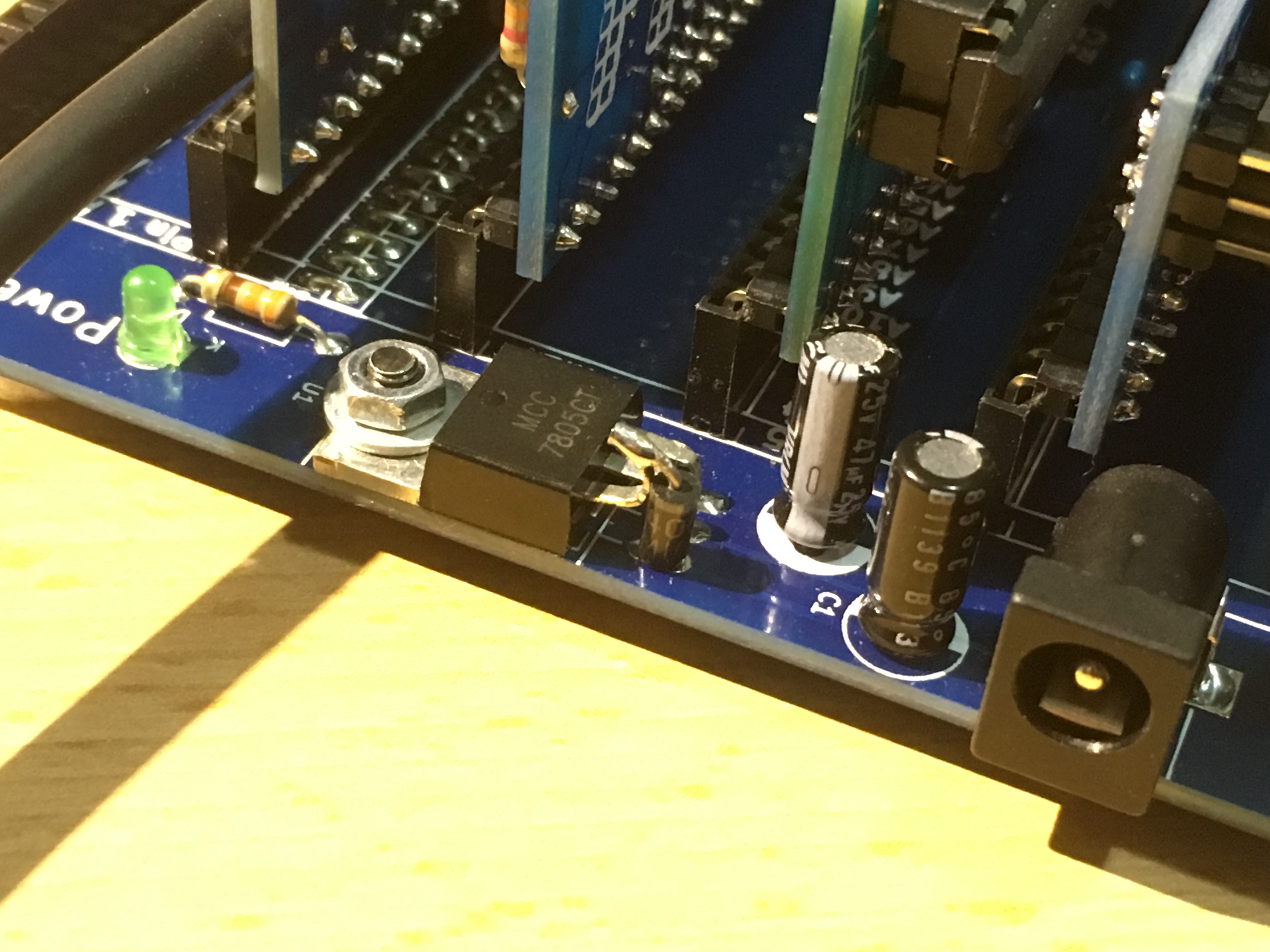
I installed a 7405 linear regulator into the provided slot on the backplane. Because there was no space for a protection diode I added one in series to the power input terminal. First, remove all of the cards from the backplane. We’ll start with power supplies. Using a 12V supply, let’s check that there is 5V and GND available to every backplane slot.
7805 Regulator with 1A linear diode in Vin.
2. Reset
I have used the new backplane Reset function. Let’s test that it is effective in providing 5V pull up normally, and pull down to GND when the reset button is depressed.
3.Clock Function
The CPU requires a Clock, and that is provided by the small PCB containing the crystal and the buffer amplifiers. I didn’t equip the Reset button or resistor on my build, because 2x resistors is not required, and only one switch was included in the materials provided.
Using an oscilloscope to watch the signal, the performance of the Clock and its crystal can be measured. So the crystal is oscillating and produces 7.353MHz with a good strong signal. And it is available across the backplane to all the slots.
[Add picture later. I’ve lost the USB stick.]
4. CPU General
Insert the CPU module and check that it has 5V power, GND, and the Clock and Reset lines are working as expected.
On the Address lines, there should be a signal at 1.232 MHz, representing the cycle of CPU running NOPs. With this signal in place, we can move on to the ROM and RAM modules.
[Add picture later, I’ve lost the USB stick.]
5. ROM & RAM
Now we check that there is power and ground at both of the ROM and RAM modules. If that is the case then it is back to the logic analyser to check what is happening on the system now that the CPU has access to instructions to read.
6. Logic Analyser
With an 8 input logic analyser we can’t look at all of the signals at one time, so let’s choose some relevant ones. The lower few address lines are interesting, because they show where the CPU is reading instructions as it starts up. Also, if the Serial I/O port is attached then the Tx and Rx lines can be monitored on the backplane too.
Reset the system to see what happens immediately after the Reset is released. Note the ASCII text message appearing on the Tx line on the backplane, noting the Geoff Seale copywrite, the invitation to choose cold or warm boot, and the memory size. This means that the RC2014 is living, but somehow the Serial I/O board is not functioning properly. So we need to focus attention there.
7. Serial I/O
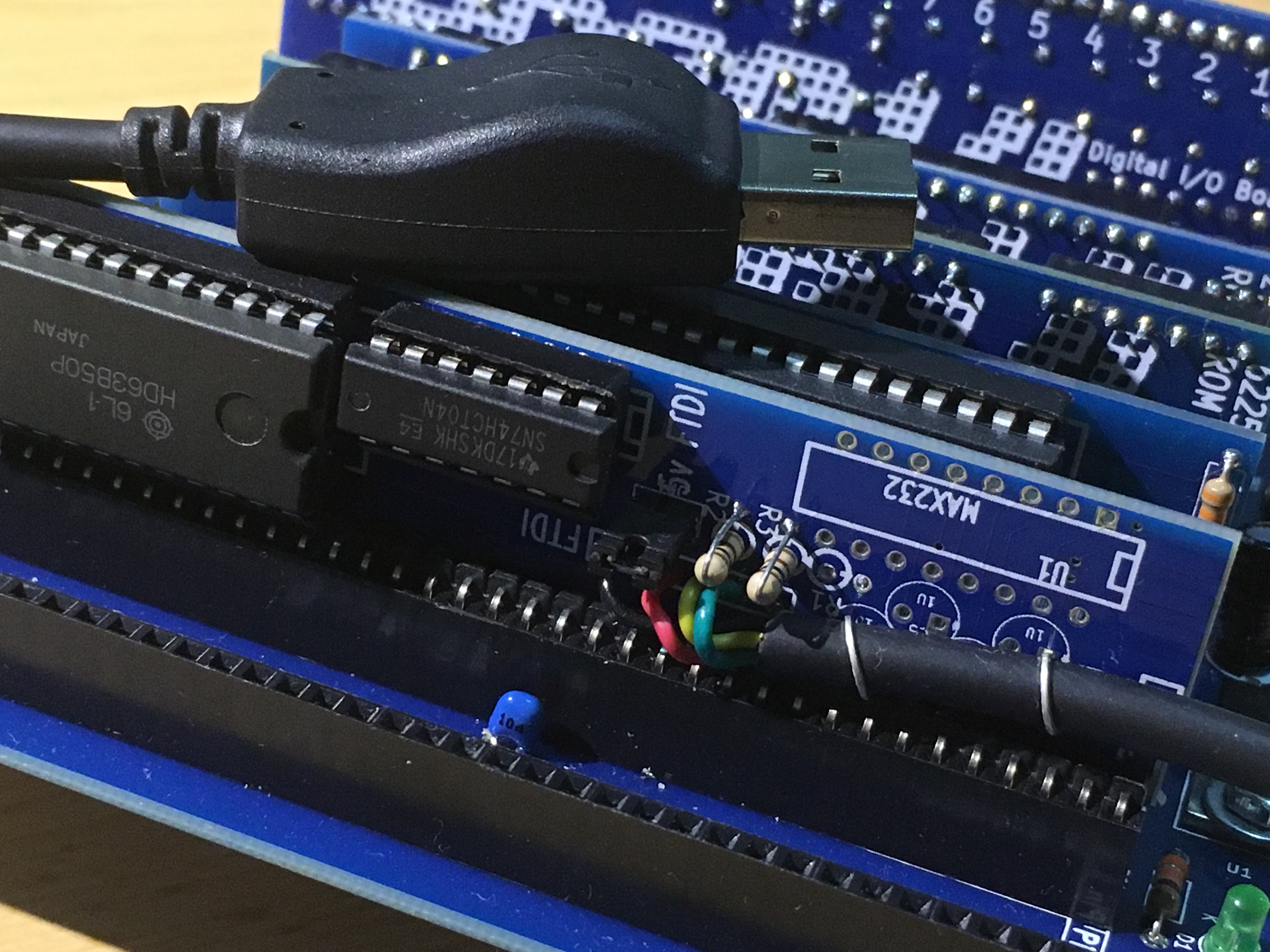
The Serial I/O card should be connected to the FTDI Basic or other FTDI FT232R equivalent device. As I had a PL2303 based serial cable, I decided to use that, as it is much cleaner than using an FTDI adapter, and it allows the Serial I/O board to be positioned anywhere on the backplane.
Prologic PL2303 Serial Cable, exits inline with backplane connector.
The Logic Analyser shows that the 63B50P chip is doing its job and producing characters on the Tx line. But we aren’t seeing characters on the FTDI Rx line on the Terminal. That is a problem. Note that there are 2.2kOhm resistors in series with the serial module Rx and Tx lines. That’s a bit more than I’d expect to see. Let’s reduce those resistors down to around 100 Ohm. They could be 0 Ohm, but it is better to be a bit conservative.
Reducing the in series resistance doesn’t allow either the FTDI or the Prologic interface to work either. There’s something else going on here.
With both the Logic Analyser and the FTDI interface attached to the RC2014 the comforting welcome from Greg Searle appears on the Terminal, urging us to cold or warm boot. Yet, when the logic analyser is removed the serial I/O is no longer working.
This looks like some kind of ground loop problem. I don’t know how this can be fixed easily. The RC2014 device only works when there is a ground provided by another source, such as the Logic Analyser.
8. Other issues
The Serial I/O device was delivered one incorrect IC socket (14 pin instead of 16 pin), so I had to solder one chip directly to the board. Not a big issue.
There is no mention of how the ROM system needs to be configured. There are three options available for selection. The right one is with all of the address lines set to 0.
The basic program is described on Greg Searle’s Simple Z80 web page. There is little mention that this this is where to go for additional software support and programming assistance.
Anyway, with the caviet that the device has to be connected with an external earth, the RC2014 is working perfectly.
9. Earth Issues
After asking Spencer for some ideas, and doing some further circuit testing, I found that I had somehow damaged the ground wire near the centre of the backplane. That was allowing the RC2014 to function when GND was provided by both FTDI and Logic Analyser on opposite sides of the backplane, but to fail when only one GND was provided.
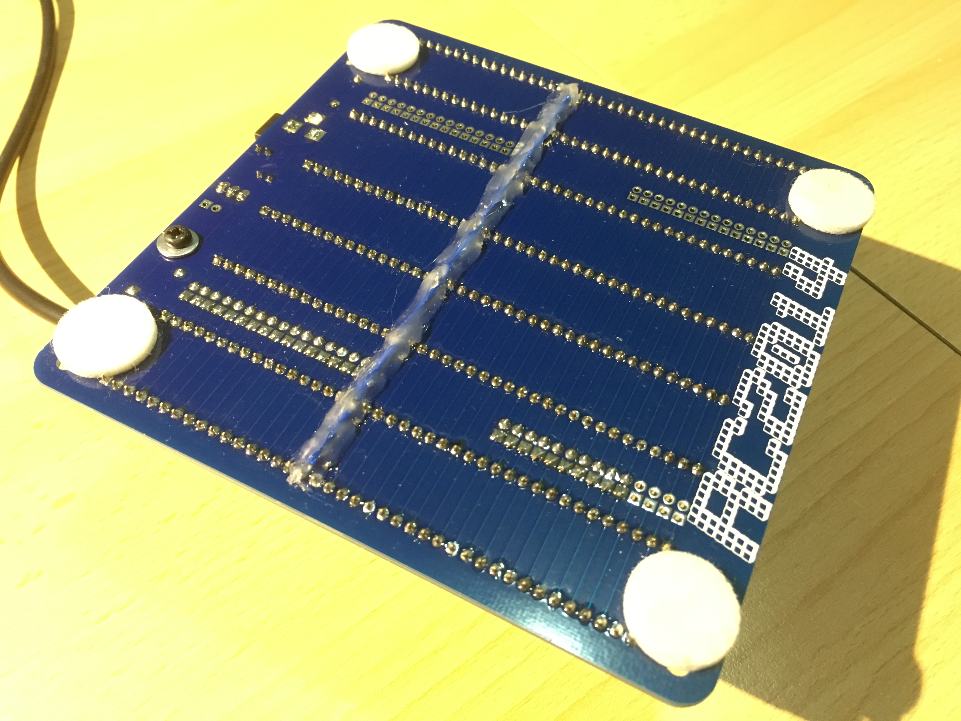
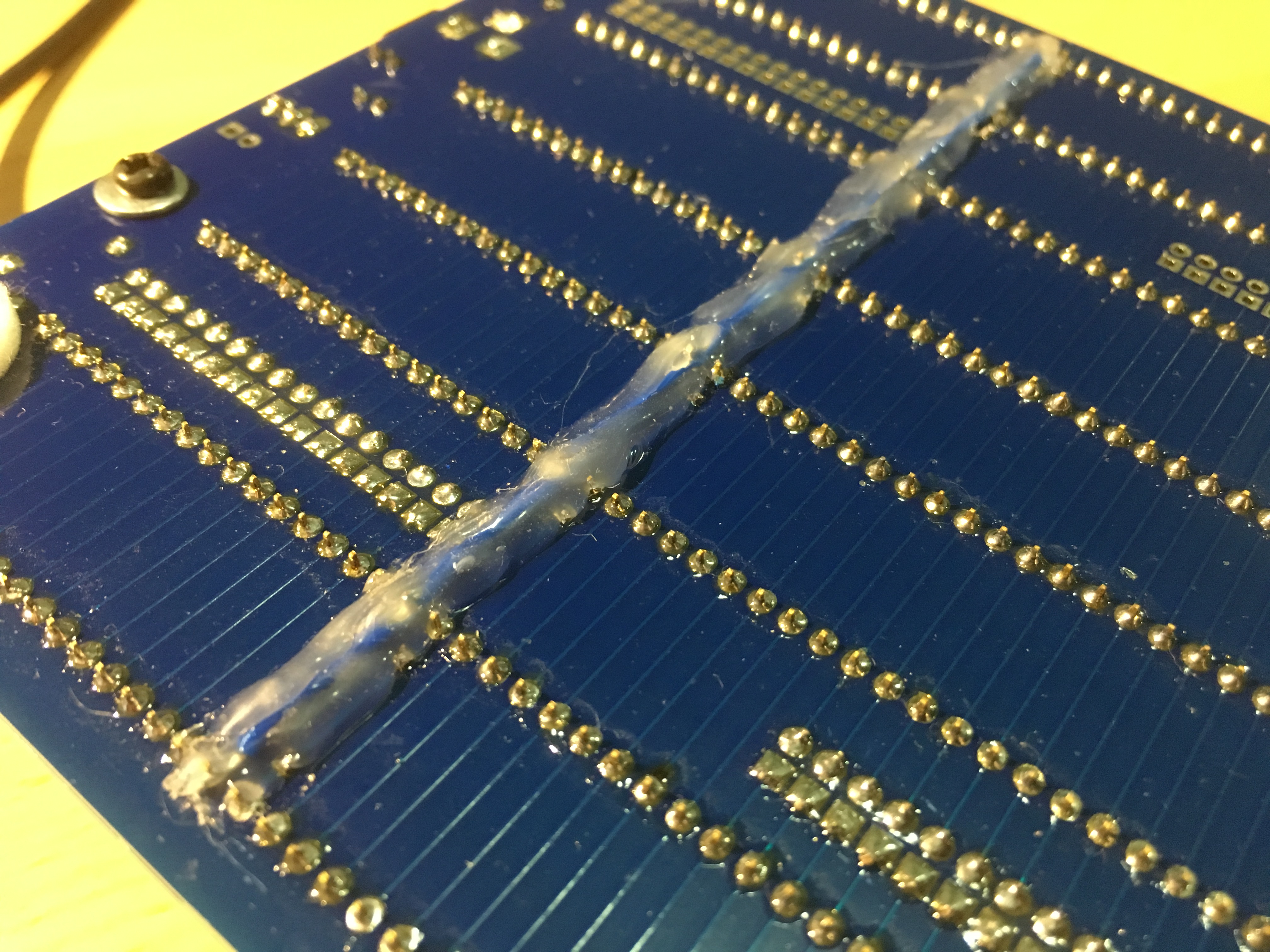
I resolved this by soldering an additional wire along the entire GND line. Whilst I could have just bridged the gap, I preferred to improve the GND stability by adding conductor all along its length. I covered the wire with hot-glue to increase its stability. As a side effect it adds a non-slip characteristic to the backplane, and helps to protect my desk from being scratched.
GND wire hidden under a protective hot glue sheath.
Now that I’ve fixed my dodgy soldering on the GND line, everything is much better, and works perfectly
The hot glue sheath helps to hold the solder pins off my desk too. Integrated non-slip.
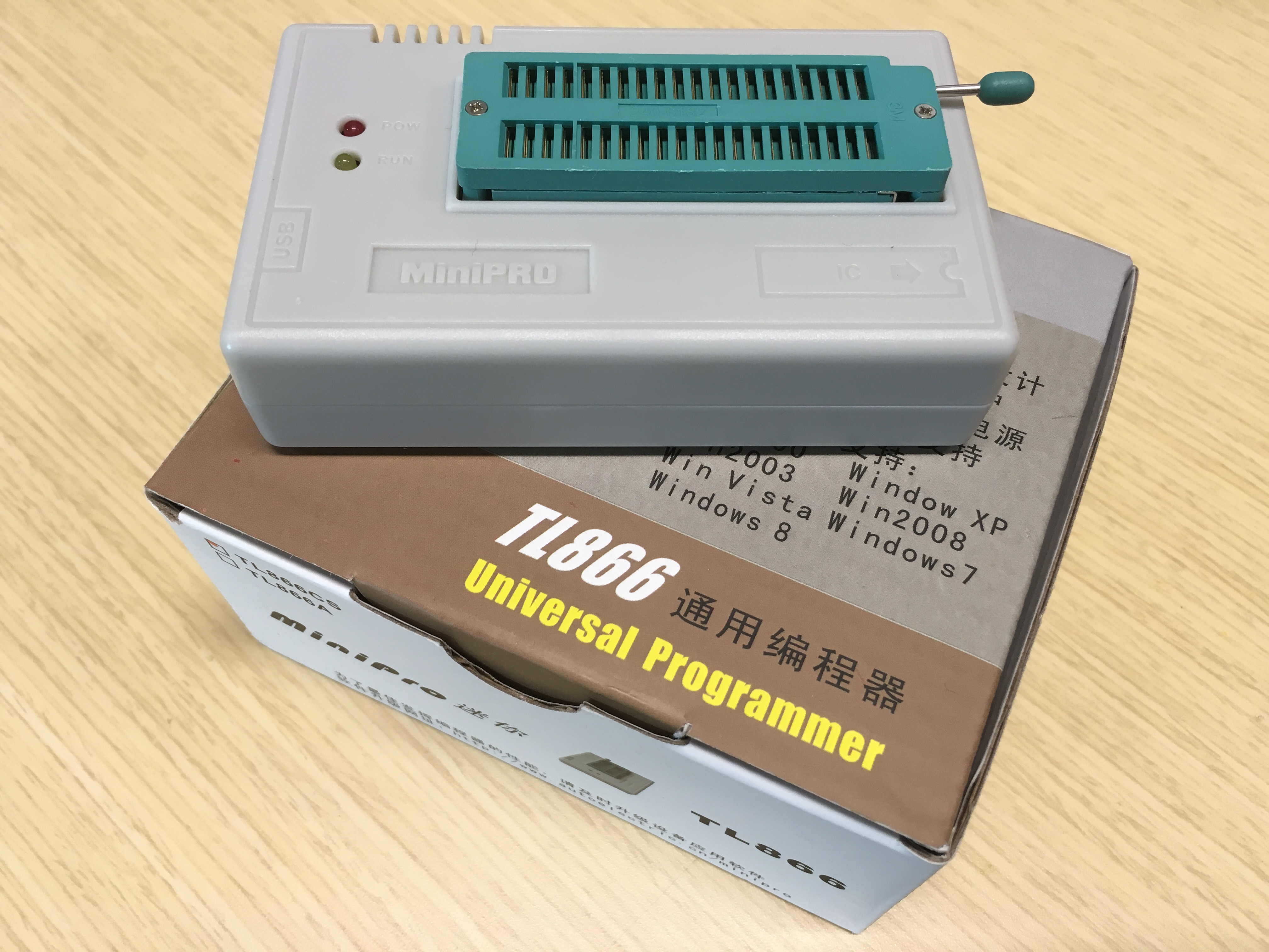
Part of the learning experience around the Z80 processor is to get a good understanding of the methods used to program the EEPROM or Flash memory used to drive old style processors. To that end, I have purchased a MicroPro TL866 programmer.
MicroPro 866 Universal Programmer
The TL866 is produced in China by the AutoElectric company. There is a web site with extensive information about the product. Many resellers exist on ebay, Amazon or other locations. I purchased mine from an ebay seller.
There are quite a number of reviews on the TL866 on the net. I skipped through the EEVblog video, read the comments, and then placed an order. There may be other alternatives around but this one is very cheap, and will meet my needs (provided it works) for the medium term.
The only choice is to purchase the version with or without the ICSP capability, for Atmel and other chips. For me that wasn’t a consideration, as I have an Atmel ICE already. So I saved my money, and bought the packaging option with multiple adapters for many EEPROM packages.
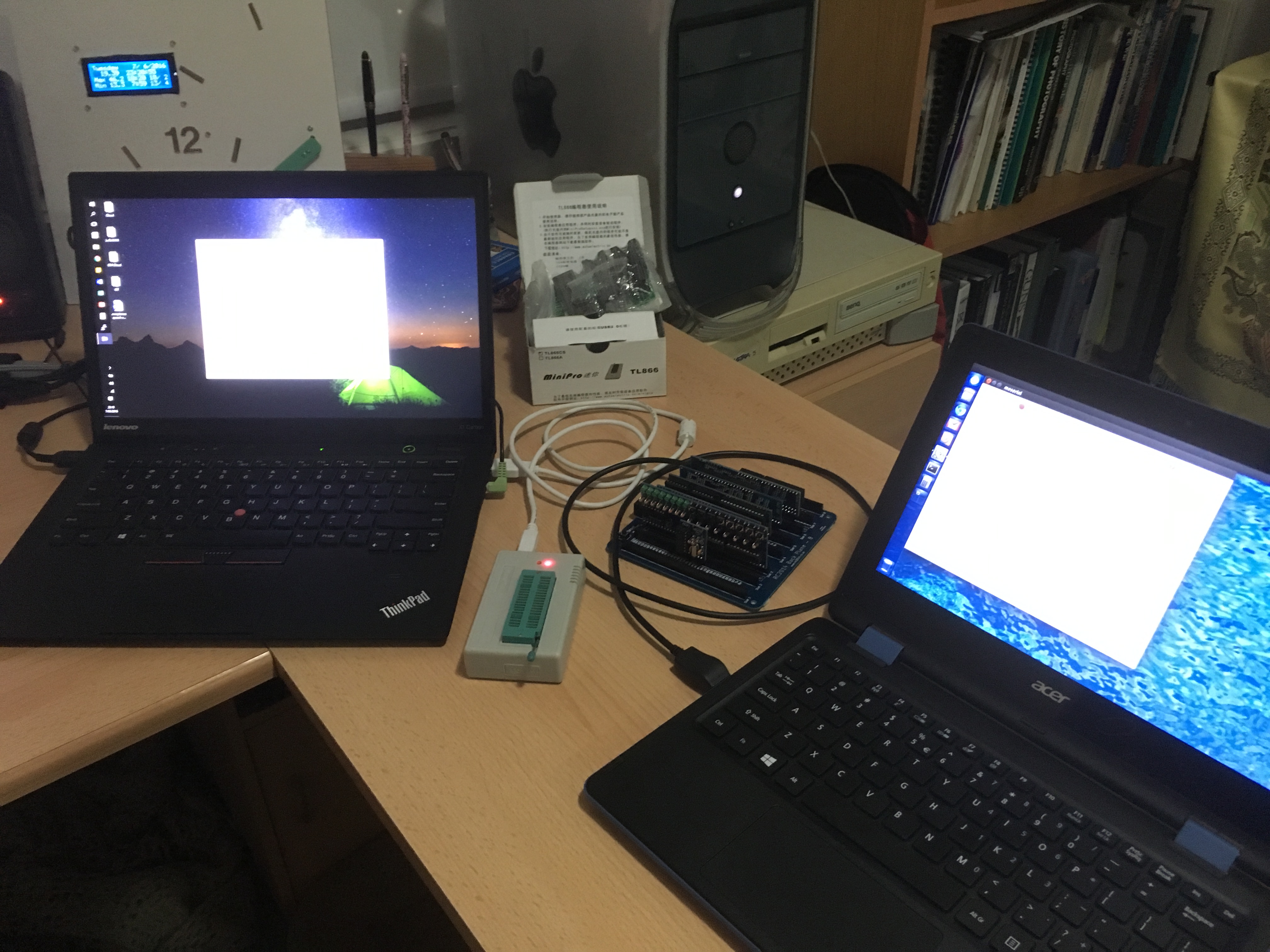
First thing I did when it arrived was to plug it into my office Windows 10 machine, and test whether it would indeed work with a 64 bit OS. I had some doubt about this, because some of the ebay sellers have not updated their descriptions to match the latest software version (v6.50 as written), which now supports Windows 10.
At home I have repeated the process with another Windows 10 machine. I’m disappointed that the TL866 doesn’t support Ubuntu or but for the small money it cost me, I can keep a second machine nearby.
Argh. I’m reminded that Windows means driver hell. I have to find a prolific PL2303 driver before i can plug in my RC2014 to test that it is working still… And of course, windows needs to be rebooted or whatever… Ok. Well that was a waste of 30 minutes. The PL2303 driver won’t install correctly. I’ll come back to that later.
Let’s test to see if we can read the EEPROM installed and delivered with the RC2014. But first, we need to download the latest version of the minipro_setup.exe program which provides the driver for the TL866.
RC2014 Cylon
Having confirmed RC2014 is confirmed working. The EEPROM is an ATMEL AT27C512R. Selecting the chip from the menu is fairly straight forward. You can search for the actual chip, or just browse for the manufacturer, if you’re not sure. There’s an Information button to show you how to insert the chip into the ZIF socket.
TL866 – Windows10 & RC2014 PL2303 Serial – Ubuntu
The next thing is to test whether the TL866 reads the chip. And, it does that successfully. I’ll save the HEX file, and then clear the chip and save it back again as the next test.
Ok so it programmed the entire chip in 20 seconds, and then verified in 1.5 seconds. Much much faster than a bootloader. Success.
As a final test, in this simple process, I selected the Grant Searle version for the 32k RAM build, to see if another HEX file could be programmed successfully. And, this works too.
So now the next step is to build an environment with C compiler and linker, to allow me to create my own HEX files to load into the RC2014. That might take a few weeks…
I’m thinking about a new project, something a little unusual but still with a rich history of information upon which to base the build. On Tindie, I found the RC2014 project which is a build of a Z80 platform but based on some modern components. That got me thinking. My next project must be a Z80 based project.
Why the Z80? Well, it was at one stage the most used CPU in the world, which leads to the great depth of information and experience available for designs, hardware, and software. Technically, it is advanced enough to avoid the need for a large number of ancillary chips, multiple power supplies, and multi-phase clocking that the 8008, 8080, and other older chips needed, but still it is complex enough that in doing a project I’ll feel like I’m actually building a computer.
This year marks 40 years (yes 40 years, since launch in July 1976) of the Z80, and still as a design and platform it looks like it will continue to be relevant into the future. So rather than building yet-another-ARM project. It looks like I will be marking the 40th anniversary of the Z80 with a new build.
An early Z80, manufactured in June 1976.
What kind of project? The RC2014 project is an interesting starting point. It is quite simple, being a compact and robust implementation of Grant Searle’s 6 Chip Z80 Computer, but provides more resources than most of the 1980’s Z80 projects offer. After looking at some projects others have done, I think that I should aim to build something a little like a “Back to the Future” Z80 project, a DeLorean (which also appeared as a prototype in 1976) with a fusion reactor.
RC2014 Cylon
As an outcome I’d like the solution to be able to interact with modern interfaces such as I2C, Ethernet, SPI, and USB, with access to a large physical memory space, with great performance, and yet retain the ability to be a single-step-able experimental platform with LED bus indicators. Single stepping is something that you can’t do with an Arduino, and it is a real differentiation.
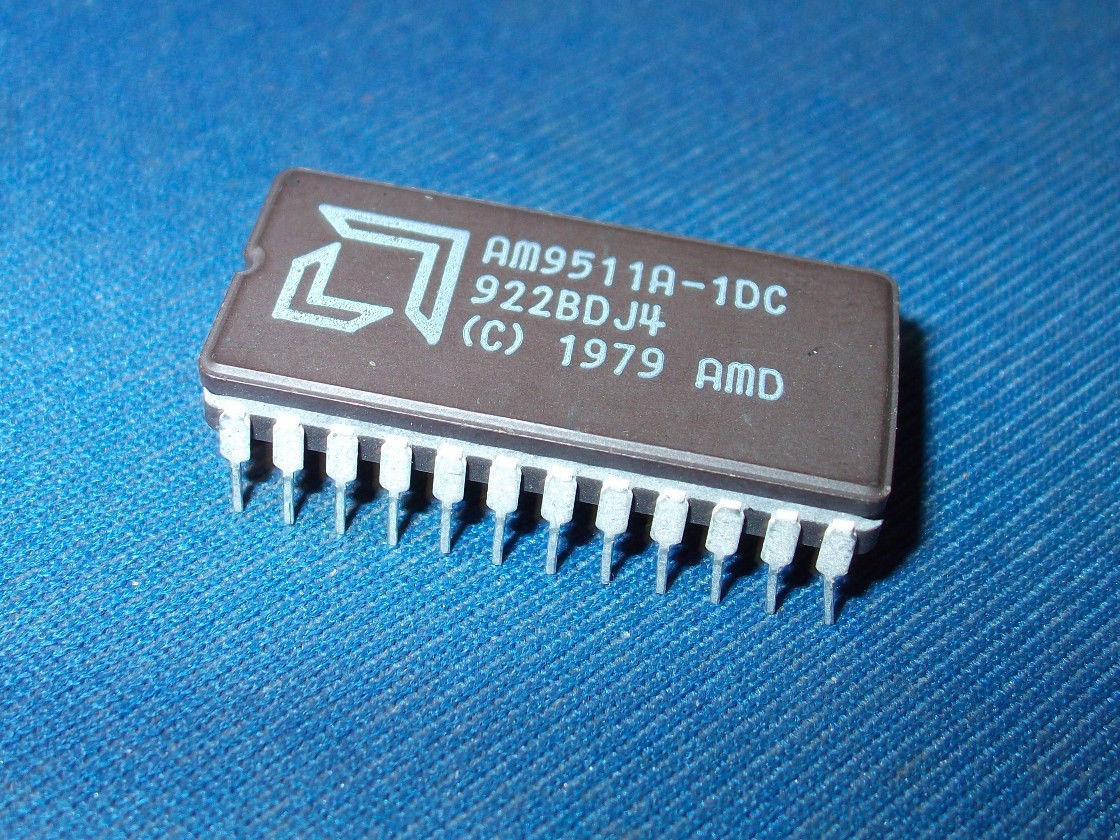
Whilst it would be attractive to design in some old-school interface devices, like the Am9511A APU or a Super I/O device, in light of today’s environment the wouldn’t contribute very much to the outcome. So the focus will be squarely on modern I/O.
Also, there is a temptation to build a CP/M system with full disk management. But again there are plenty of CP/M systems around. I’d like to build something more of an embedded platform, that doesn’t require mass storage to run applications. It would be good if most of the basic interfaces could fit on one board, to avoid the need to build address and data bus extension. I think this will simplify the design significantly.
Design process
This is going to be an iterative process. The first step will be to build the RC2014 project, and test that I can program it.
RC2014 Cylon I/O
RC2014 Serial I/O & CPU
It will be important to learn a little about Z80 assembler. Later, I may modify the RC2014 project platform.
Then, I’ll lay out a through hole prototype with minimal functionality, to test some performance ideas. If they work on through hole, then they’ll work with SMD. Using through hole also allows me to quickly fix logic or wiring errors that would take a new spin with SMD.
Finally, I’ll build a SMD device that miniaturizes the solution, and makes it more robust.
Processor selection
The Z80 has been built continuously for 40 years, and in that time many manufacturers have produced silicon and several clones have been created. The Z80 range been continuously improved through the Hitachi 64180, to the Zilog Z180, and the Zilog Aclaim eZ80 devices. Each increment has integrated more accessory components, and improved the instruction throughput, as well as increased the clock rate.
Looking at the options available, the original Z80 requires logic to get started. So rather than building serial ports and timers, it looks like the Z180 might be the right place to start. So why not go all the way to the eZ80? Well the eZ80 is not dissimilar to an AVR ATmega device, with all of the system components integrated into the one device. Using an eZ80 CPU wouldn’t be like building a computer at all. It would be much more like building an Arduino, and I’ve been there already.
Out of the Z180 options, I would select the Z8S180 (at 33MHz) because it integrates sufficient material to get started (Timers, Interrupts, MMU, & USARTs), and leaves me the option to add complexity as I get going.
Memory selection
A little research on the processor and available memory provides me with some cornerstones for the design. I will use Flash memory for the program storage, and static RAM for the system memory. Historically, UV erasable PROM and dynamic RAM would have been used. One advantage of static RAM is that the solution is fully single-step-able. Meaning, I’ll be able to watch the address bus and data bus process each instruction as the Program Counter marches along.
The Z180 can address up to 1MB of physical address space, and it makes sense to provide the full physical memory possible. The price of 1MB of SRAM or of 256kB of Flash is almost nothing these days. As the Z80 logical address space is only 64kB, the Z180 has an inbuilt MMU to manage its physical memory to logical memory mapping.
Memory mapping
NOTE 2017 October: The details in the below discussion are no longer accurate. The memory design has moved on substantially, but this discussion remains for information only. Happily, even completely changing the memory mapping can be done with a software reconfiguration of the Memory / IO logic device.
To keep things simple (in hardware), we can use the MMU available in the Z180 to map the physical memory locations on 20 address lines, into logical addresses that suit us. The MMU can map 4kB pages of physical memory into two relocatable logical locations in the Z80 logical address space. These are called the Banked and the Common 1 locations. The Common 0 memory location begins at physical address 0x00000, and continues to the beginning of Banked memory, which then continues to the Common 1 memory address space.
Therefore the hardware (or physical mapping) will show that the 256kB Flash is located from 0x00000 to 0x3FFFF, and the 1MB RAM from 0x00000 to 0xFFFFF but the lower quarter of the RAM address space mostly masked by Flash. For programming we’ll have to move this around.
When the Z80 starts up it always begins from physical and logical address 0x0000. Therefore it is typical to put the program storage in the lower address range, and the RAM in the upper range. Given the use of the MMU available in the Z180 we initially can map the SRAM into the upper 32kB of logical address space, using the Common 1 bank and CBAR setting, leaving the first 32kB of Flash in the lower address range.
One difficulty is that there are only 3 memory spaces available, so if we want to have a C stack, global buffers and queues, and global data, then we need to put some SRAM in the Common 0 address space. Let’s uncover 8kB of 1MB SRAM and place this from 0x2000 to 0x3fff to provide this C stack and global variable data frame.
At some stage I assume I’ll want to use all of the additional Flash and SRAM available, so I’ll have to integrate programming for MMU bank switching, and RAM heap/stack switching when the need arises. At least initially there will be a statically programmable range of between 8kB Flash with 56kB SRAM to 56kB Flash with 8kB SRAM available within the logical address space, depending on the MMU initialisation settings.
To program the Z180 with a soft programmer, the physical memory addresses will need to be juggled around (glue logic) to disable the Flash and SRAM from appearing in the first 8kB Bytes of the address space. The USB soft programmer will provide program codes in the form of a remote boot-loader to load the contents of programs into the Flash, by moving the entire physical flash through a 4kB or 8kB Banked page. SRAM located in the lower 32kB address range will be loaded with a program to enable buffering and page writing of the desired programs.
Physical Address Range
Run Mode
Programming Mode
$00000 – $01FFF
Flash (8,192B of 256kB)
USB (8,192B)
$02000 – $03FFF
SRAM (8,192B of 1MB)
SRAM (516,096B of 1MB)
$04000 – $3FFFF
Flash (245,760B of 256kB)
$40000 – $7FFFF
SRAM (768kB of 1MB)
$80000 – $BFFFF
Flash (256kB of 256kB)
$C0000 – $FFFFF
SRAM (256kB of 1MB)
Logical Address Range
Run Mode
Programming Mode
$0000 – $1FFF
Flash (8,192B, Common 0)
USB (8,192B)
$2000 – $3FFF
SRAM (8,192B, Common 0)
SRAM (24,576B, Common 0)
$4000 – $5FFF
Flash (8,192B, Common 0)
$6000 – $7FFF
Flash (8,192B, Banked)
$8000 – $FFFF
SRAM (32,768B, Common 1)
Flash (32,768B, Banked)
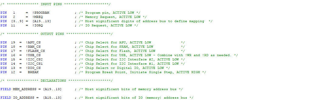
The programming mode (address mapping) will be entered by either a button press, or by signalling from the USB – USART interface lines. The process is to invert the Address 19 line, shifting the physical address location of Flash, and mute Address 0-12 to prevent memory being read from these locations, which allows the USB – USART FIFO to provide program opcodes. Mute by disabling the CE on both Flash and SRAM when A13 through A19 are 0. Then configure the MMU to bring the Flash into Banked logical addresses, using the SRAM to buffer 4kB page writes to Flash memory.
Using the ATMEL WinCUPL tool, it is pretty straightforward to convert the above memory mapping and below logic mapping in CUPL language description to JEDEC format that can be handled by a MiniPro TL866 EEPROM & PLD Programming tool, and programmed into an ATF16V8C or Lattice GAL16V8D device.
CUPL Memory / IO Definitions
CUPL Memory / IO Decoding
This memory and IO mapping needs to be augmented by a secondary logic mapping for managing programming, single step, and other functions, which will be programmed into a second ATF16V8C or GAL16V8D device. The logic mapping will allow automatic programming initiation via the FT245R USB interface.
CUPL Logic Definitions
CUPL Logic Decoding
Using EEPLD devices will save significant PCB real estate, and will allow me to compensate for minor logic errors after the fact.
Schematic for Memory GAL
Schematic for Logic GAL
FCPU selection
The best Flash memory we can get easily is 55ns timing. This is bettered by SRAM, with 45ns access timing. By converting this timing to a bus frequency we can achieve 20MHz or slightly better, but allowing for some buffering or address logic delay it would be better to keep the system bus under the equivalent of 20MHz.
Using this system bus speed of approximately 20MHz then poses a question; which is the right speed? Some references point out that the Z180 is very poor at holding the correct USART rate when the CPU clock is not a magic multiple of the USART rate. This is the same issue that the AVR ATmega device faces when its USART is not driven by a magic frequency clock. Therefore, lets us set the CPU crystal oscillator to 18.432MHz, being most appropriate magic frequency for the following design.
The Z180 system clock (or PHI) can be double, equivalent, or half the rate of the crystal oscillator base rate. Starting with 18.432MHZ oscillator clock, depending on the CPU Control Register (CCR), the system bus clock (PHI) can be halved and is operated at 9.216MHz. This is slow enough to allow most peripherals to interact with the CPU. Internally, the system bus clock (PHI) can be doubled to operate the CPU at 36.864MHz, by setting both the Clock Multiplier Register (CMR) and the CCR. This rate is slightly overclocking the Z180, but that’s what we live for. We don’t build slow computers.
As we are using 45ns SRAM and 55ns Flash, we will have to insert either 1 or 2 memory wait states when operating at 36.864MHz. This is unavoidable, because of the access speed of both memory devices. Faster SRAM may be available, but faster Flash is quite hard to obtain.
I/O Mapping
I have been thinking about the whole idea of system modularity. Actually, I don’t think the traditional method of building a backplane is such a good idea for what I want to achieve. Extending the address bus a long distance means that I’ll be investing in design and timing issues, that I’m not really sure I know how to solve. So, let’s focus on a smaller design, with on just one board for the time being.
As a computer always needs to be extended and interact with the real world, I think it would be good to add modern user interfaces to the solution. Use Address 15-13 to provide I/O selection options on the CPU Board, using the remaining output pins from the Memory ATF16V8C or GAL16V8D. This will allow flexibility to latch data into the Hex Display, or trigger breakpoints using #M1 and #Wait to allow Single Step execution from any code point.
Single Step – The Z-80’s #M1 pin is useful for building logic to single-instruction step the machine. You do this using the memory ready signal on #M1 to clear a 7474 flip-flop, which is clocked by a Single Step signal, to produce a #WAIT signal for the CPU. That stops the machine on the opcode fetch cycle with the address showing on the address bus and the opcode byte showing on the data bus. To move the machine ahead, you clock the flip-flop which releases the #WAIT signal, until the next #M1 clears the 7474 again.
I2C interface – This is the most important interface, which provides many extension options, and a plethora of Grove System sensors. Unfortunately the 5V nature of the system precludes using the newest really fast, deep buffer, devices with multiple bus I2C 1MHz bus interfaces, so provide 2x devices to support different applications (eg. video output and sensor acquisition on separate buses). Use the #INT1 & #INT2 interrupts.
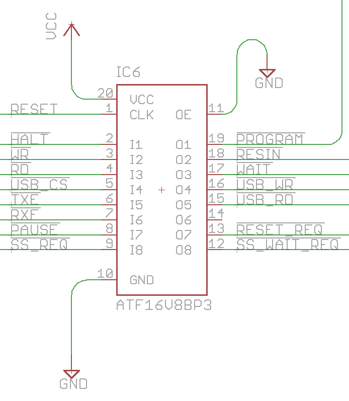
Arithmetic Processor Unit – This lovely old chip is now also 40 years old, and was the world’s first APU (or FPU). Potentially, it is too slow to contribute, but still we’ll build it in. Need to provide a 3MHz clock to drive it (FAPU = FCPU/6), and connect its #PAUSE to #WAIT. #END connected to #INT0. RESET is ACTIVE HIGH.
Ethernet – Wiznet W5300 Direct address mode requires 3FF of address space. Configure the #INT0 interrupt and implement the DMAC1 I/O to move packets quickly. Exclude this from the initial build, as it is quite a complicated 100 pin device, and it needs 3.3V supply.
USB & SPI interface – provide mass storage capability using either USB or SPI interface devices. The CH37x series is not very well documented, or readily available. There are other options for I2C-SPI bridging which can provide an SPI interface if needed.
CH376S – Incorporating the USB functions as described in CH375, and CH372
ADC interface – Better, higher resolution, faster chips are available with I2C interfaces.
8 bit ADC with internal reference MAX158 – Digikey MAX158ACPI+-ND
Video Interface – Can be done using an external I2C device.
Super I/O – Floppy Disk & IDE Controller – Too hard and doesn’t bring much value to the table. Floppy drives are hard to find, and there are already 2x USART ports available on the Z8S180.
Well quite a few iterations on my aspirations and thoughts have resulted in a YAZ180_v1 schematic, that I think is now basically frozen. Some of my design decisions follow.
After deciding not to use the TIL311 LED display devices because they are not easily obtainable, I found the alternative solution using the DM9368 display driver chip and LED display devices was very consuming of space on the board. Since the board had to be no greater than a maximum of 10cm by 16cm to fit within the constraints of my Eagle Hobby licence, I decided to buy some TIL311 devices in advance, and then with the comfort of stock in hand I could use them for the design. Also, they add significantly to the retro-chique.
I would have loved to add the Wiznet W5300 device to the design to provide high speed Ethernet capability, but with a 100 pin VLSI it was just too complicated for the initial design. Next time.
I added a 82c55 interface chip. Knowing that it is very slow, requiring 2 wait states to drive it, is one thing. But the advantage of having multiple latch-able input and output ports, off one fairly compact integrated device made up for that problem. As it is a 1970s device it is also retro-chique accretive.
Designing using CUPL and the Atmel or Lattice PLDs is in my opinion much simpler than tracing schematics and thinking through 7400 series NOR, NAND gates to get the desired addressing logic. Writing the logic in “c” like syntax is much less taxing on the brain.
After deciding to implement no bus drivers, and then building a solution adding drivers and termination to every address and data line, I have rationalised down to bus drivers on data, lower address, and control lines. These are the few lines that appear on all memory and I/O devices, and are taken to every point on the board. The upper address lines only appear on the PLD, SRAM, and Flash, which are very low load modern devices, so there is no point to buffer them. Using ABT logic limits the differential delay on the address lines to 2 ns, and since the read and write select lines are also buffered, there is no issue timing issue created.
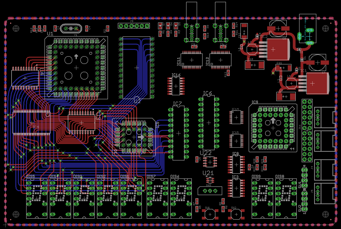
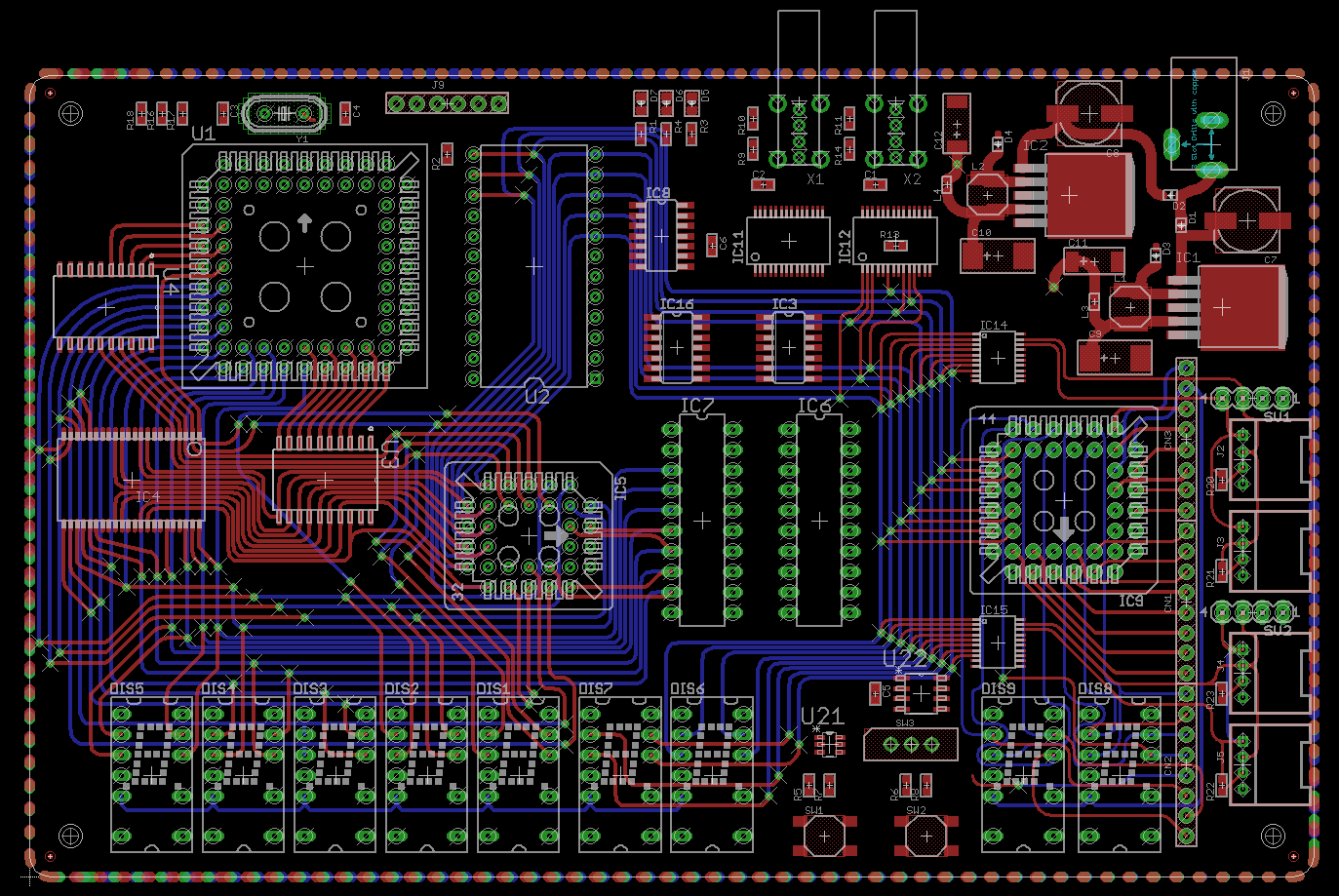
And here is the first schematic, in pdf YAZ180_V1. Errors and omissions did occur.
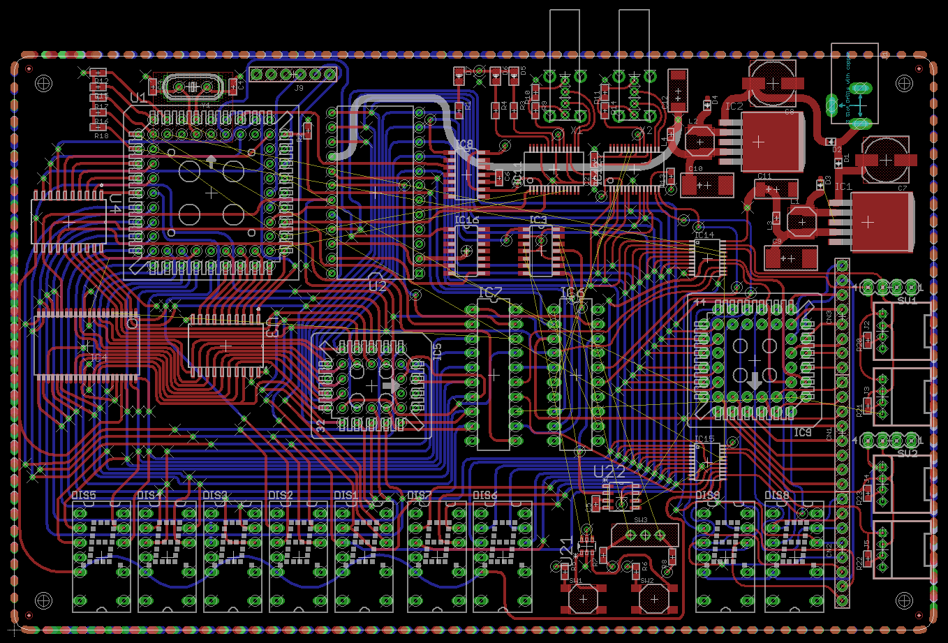
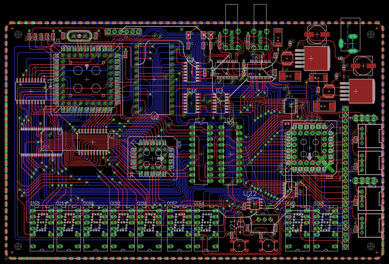
Hardware Layout notes
With the first major layout session behind me, I have the following notes.
Address & Data to SRAM and FLASH
Change the SN74ABT244 for the SN74ABT541. The only difference is the pin ordering, with the 244 being optimal for counter-flowing signals, and the 541 being optimal for unidirectional signals (physically). This will help layout.
Getting 20 address lines and 8 data lines to appear on the SMD SRAM memory is challenging. I will probably reassign the address lines to suit the Z8S180 pin-out, rather than spending hours untangling the lines. It won’t be too easy to do this with the Flash device, but as it is in a PLCC through-hole socket it comes inherently with “vias” making reaching it half as hard as SMD.
Input pin and I/O pins on Z8S180 include weak latch circuits to prevent excessive current draw by the receiver, if the pin is not externally driven. External pull-up or pull-down resistors should not be less than 15 kOhms to ensure that the resistors can control the state of the latch when power is supplied.
All Address and Data lines routed.
A few more air-wires remain, that will need thought.
Following about 10 hours of juggling, just two wires remain together with a plan to resolve them tomorrow.
Just two air-wires remain.
Finished, except for the detailed checking, which usually results in some changes. But, it is done.
The screen grabs below show with the Vcc Layer in Grey, and GND Layer in Green. I have added some basic traces on those layers to close off the routing, which are misleading. The layers are actually completely filled, normally.
This slideshow requires JavaScript.
Bill of Materials
Well, building this retro-computing machine is not quite as cheap as an ATMEL micro-controller board. But then again, it is not quite in the same league, with 1MB of RAM, and 256kB of Flash storage, together with an APU and 9 digits of LED display.
I have ordered all of the components, except the Am9511A-1 APU and the TIL311 LED display devices, from Digikey. The BOM is detailed in this link. To add to BOM, this there are the Am9511A-1 and the TIL311 devices which can be found on eBay or other auction sites.
And, the PCB looks great!
Bringing up the Prototype
The build and bringing up of the board will continue, once I get the new SMD oven sorted out.
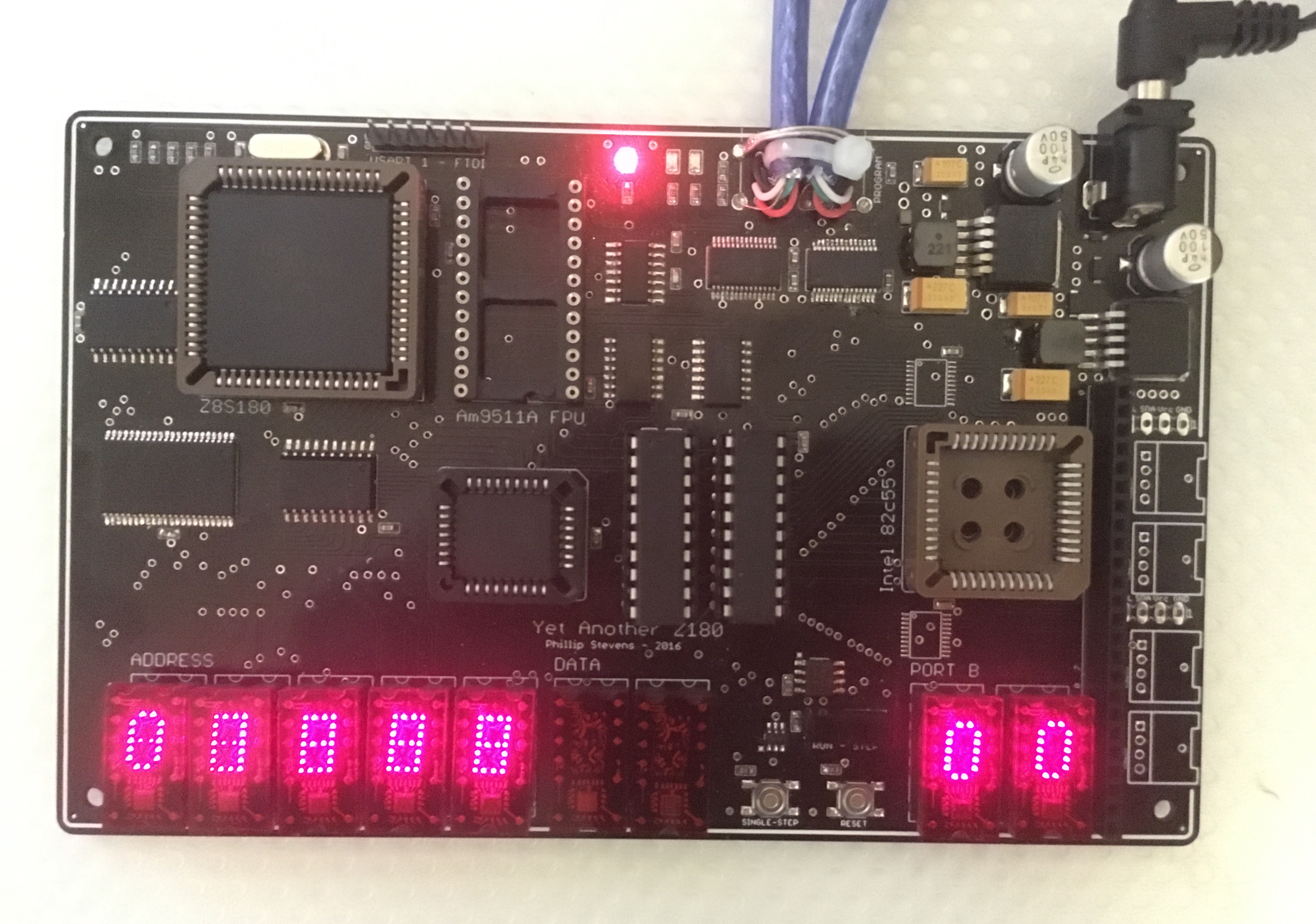
Well, the board has been soldered, and everything looks good. The SMD oven wasn’t as useful as I thought. It turns out that I can solder the fine pitch of the SRAM and FTDI devices fairly well with a normal soldering iron.
My PLD programmer won’t work with ATMEL devices, so I’ve been waiting so long for some Lattice GAL devices to be shipped to me. Over 8 weeks in transit. Finally they’ve landed. So I soldered the rest of the board together.
I’ll have to debug my CUPL programming of the GALs to get everything working, but at least there’s no “magic smoke”.
The TIL311 LEDs are very hot, because they draw so much current. LEDs really have come a long way in efficiency over the past 30 years.
Update 9 Jan 2017. Using this Github Repo, I’ve successfully sent characters to the ASCI. It lives!
Update Friday, January 13th 2017. Initial RAM testing passed!
And now based on this testing, I’ve been able to get the ASCI0 (and ASCI1) working, so that I have NASCOM BASIC Ver 4.7 (1978) running on my 2016 designed computer!
This is a Mandelbrot program running in NASCOM Basic v4.7.
Glowing, in a dark room.
Three major items remain to complete, before a PCB revision.
Completing the “in circuit programming” tools, to programme the Flash memory without removing it.
Writing drivers for the Intel 82C55 PIO device.
Writing drivers for the AMD Am9511A APU device.
Following the PCB revision, I’ll work on the I2C platform, and its drivers.
Next up, programming Flash memory using the FTDI FT245 USB-Parallel port. This was working, but some bad soldering made the on-board FT245 inoperable. Testing was completed using an external device.
Testing for the 82C55 PIO device is now done. It can do a lot more than this, but the proof of life is completed. Time to move on.
Update February 20, 2017. Despite initial misgivings, that the Am9511A APU was wired incorrectly, the proof of life for the APU is now done.
For a long time, I could see that the APU was trying, but just wasn’t making it. Two issues were involved.
Firstly, all of the datasheets assume 74 logic is being used to create the chip select from 3 to 8 address decoding, or similar solutions. What they don’t point out is that the Am9511A APU chip select MUST be generated from the address lines, because the Z80 (Z180) IORQ line has incorrect timing to drive the Am9511A. The Am9511A needs an 30ns of chip select and address validity after WR is raised, which the Z80 IORQ timing doesn’t provide. Having infinite logic in a GAL available, I had (incorrectly) included the IORQ line in the APU_CS logic. Whilst I’d recognised the issue, it took three lines in an obscure 1981 PhD dissertation to focus the spotlight of clarity. Thank you Mr Haining.
Secondly, the Am9511A samples I have on hand won’t work at 3.072MHz. I guess they were cutting very close to the limit in the day.
YAZ180 v1 full configuration.
I’ve finished an initial revision of the PCB to fix all of the known errata. I’ll sit on it a bit until I can double check that everything is good.
Errata
The power supply section was done very simply in the V1 build. I underestimated the requirement for 5V power, thinking that 1A should be sufficient. Before I built the V1 board I realised my error and replaced the 5V 1A regulator with a AP1506 that can supply 3A. I also changed the inductor to a lower inductance and higher current version.
I’ve now revised the power supply section to use LM2596 3A device for the 5V supply, as this device has a larger input voltage range (up to 40V) , and I have inserted thermal vias to improve the heat spreading into the back side of the board.
The 12V supply only needs to provide about 90mA for the APU. I’ve reduced the capacity of the regulator down to 500mA, and have saved some space by using a LM2674 in SOIC-8 format. Whilst the Am9511A gets uncomfortably warm, the power supply doesn’t.
Also, I simply forgot to provide a 3.3V supply, that is required for the I2C interface devices. So this has been repaired with a 1117 linear regulator, supplied by the 5V regulator. It is the same device I used in the Goldilocks Analogue as I have some parts in hand.
I’ve swapped the USB connectors to male versions. Can’t understand why I built YAZ180 V1 with female connectors. Just silly.
I’ve swapped the location of the RESET and SINGLE_STEP buttons. It makes more sense to have the buttons doing the same function closer together.
The Z8S180 requires that its DCD0 be held low, before the USART0 can transmit. This pin is now tied to GND.
The Logic GAL device, in Registered Mode, requires to have its OE held low. This pin is now tied to GND.
To generate a RESET signal, the reset request input to the Logic GAL can’t be on Pin1 in Registered Mode, so the RESET_REQ signal was moved to Pin14. Pin1 in Registered Mode is connected exclusively to the CLK for the GAL flip-flops. In order to clock the flip-flop implemented in the YAZ180 programming mode logic, the RESET line was connected to Pin1.
The Am9511A-1 although specified at 3MHz, doesn’t pass tests at 3.072MHz. So it will have to be de-rated to 1:8 from the Z8S180 system clock. This takes the clock speed down to 2.304MHz. The clock divider chip will be replaced by a sn74ls93 from Digikey 296-3749-5-ND.
For the purposes of enjoyment, I’ve connected the Z8S180 DMA engine DREQ1 and TEND1 lines to the Am9511A SVREQ and SVACK lines. The SVREQ requires a NOT to generate the inverted Z8S180 signal for DREQ1. Although there are very few bytes loaded into the Am9511A, this should allow them to be written by the DMA engine.
Both AMD Am9511A and Intel 82C55 need the address and chip select lines to remain valid for a period after the RD or WR signal has gone high. Therefore we need to remove the existence of a valid IORQ signal from the calculation of their select line, and just rely purely on their address decoding (and absence of MREQ). The CUPL coding has been adjusted
The Am9511A supports 1 I/O Wait State, as RD & WR to Pause is 100ns. The 82C55 requires 2 I/O Wait states, as RD is 200ns minimum.