
The 8080 CPU stands at the root of microprocessor development over the past 50 years. Although it was the first commercially successful device, it was followed quickly by two different processors with different bus characteristics. This is a record of interfacing one of the descendants, the Intel 8085, with peripherals and modules designed for use with the other descendant, the Zilog Z80.
All three of these devices, the 8080, the 8085, and the Z80 were implemented with 40-pin DIP packaging, which limited the number of pins they could use for bus signalling. The 8080, requiring 3 power supply voltages, was particularly limited as it didn’t multiplex the address or data lines, but rather needed to share the data lines for status information. More about the 8080 can be read at Wikipedia, or CPU Shack. I will not add to it here.
Derived from the 8080 and implemented by the same lead designers and architects, the Zilog Z80 uses four lines to signal general timing on the bus. In addition, a M1 line is used to signal that an interrupt is being processed and that an interrupting peripheral needs to provide an address (or vector) to which the CPU should jump in IM2 mode.
The Z80 rationalised the power requirements down to +5V and GND, which allowed a simpler and more explicit set of bus controls to be provided. As the Z80 implemented two address spaces, one for memory and one for Input/Output ports, it was useful to have two separate lines signalling memory access and Input/Output access. In this way a peripheral only needed to handle one of the two signals, depending on whether it was memory or a I/O address space peripheral device.
In addition the Z80 has two lines providing signalling for Read or Write. The timing was designed so that the data on the 8 data lines was valid at the point when the respective signal was deasserted. The Z80 would hold data it wanted to write or output until the write signal was deasserted, and it would latch and read the bus when reading or inputting data when the read signal was deasserted.
With only minor differences, the Memory and Input/Output lines are operated with similar timing, and this is aligned mostly with the Read and Write signals. This enabled system designers to build very simple bus interfacing for their Z80 based systems.
There are many additional features and alternatives here, around Interrupt Mode 2, timing for sampling the Ready pin which causes the Z80 to pause, and other minor timing issues. However, they are not relevant for most purposes.
Most system designers used these four signals to create memory write, memory read, I/O write and I/O read signals. Then one signal line, together with a chip-select generated by the address lines (directly in simple systems, or through logic in more complex systems) was enough to operate each component of the system.
For the 8085, the Intel architects took the bus interface in another direction. They integrated several components from the support chips for the 8080 into the silicon die, and produced new features which made the 8085 much more useful as a micro-controller than the Z80. For the bus, the major change was to multiplex the data lines with the low address lines. This step allowed them to reuse the 8 saved lines on the 40-pin DIP for other purposes.
Multiplexing the address and data lines meant that they had to add an external address latch, to capture the lower address values, before either writing data or reading data from the bus. The normal read and write lines are present and they behave in a similar manner to the Z80.

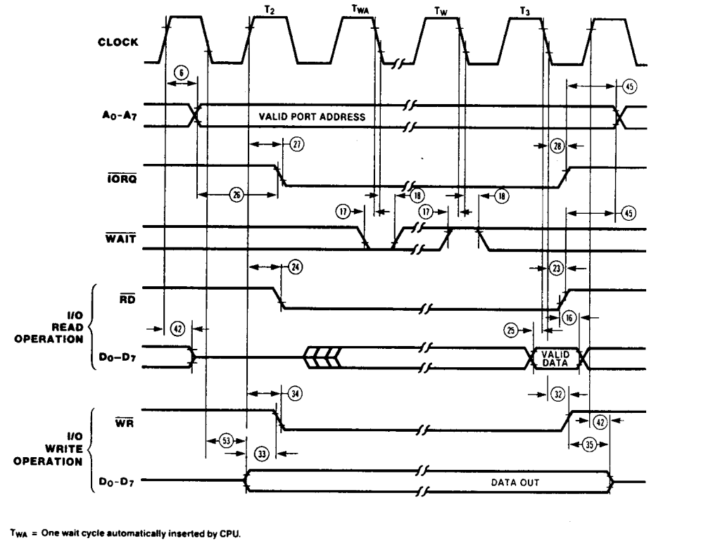
In a significantly different solution to the Z80, the 8085 uses only one line to differentiate Input/Output and Memory addresses. Using the sense of the line high or low to indicate whether the I/O address space or the memory address space is being addressed. The timing on this IO/M line is also substantially different to the Z80, where here it is valid for the entire cycle of an instruction. It does not become valid when the bus address is valid, rather it is valid from the start of the instruction through to the completion of the instruction.

This is the first significant divergence from the Z80 system bus, and it causes issues with peripherals that require an enabling signal to be provided after the address lines are stable. In most designs a decoder was required to produce signals for attached peripherals.
Generating Z80 /IORQ and /MREQ from 8085 signals
As many Z80 standard peripherals and also Motorola peripherals need to have the /IORQ line valid when the address is stable, we need to generate a Z80 compatible /IORQ (and /MREQ) signal. There are textbook “decoder” circuits available to produce the four system signals /IOR /IOW, /MEMR and /MEMW from the 8085 IO/M signal and /RD, /WR, but there is no standard solution for using the 8085 on the Z80 bus. This problem we are going to solve.
From the Z80 datasheet the /IRQ and /MREQ signals are almost exactly tied to the timing of the /RD and /WR signals. Therefore we can use /RD and /WR with some combinational logic to produce mostly correct timing for /IORQ and /MREQ. We need to have a valid signal when either /RD or /WR is low (active). If both are high, then the result should be also high (inactive). Both /RD and /WR are never active, but for convenience we can let the result be active if both are. In positive logic this would be generated by an OR gate. But with inverted logic (active low) this is implemented as an AND gate.
| /RD | /WR | Result – /RD./WR |
|---|---|---|
| 0 | 0 | 0 – Invalid state. |
| 0 | 1 | 0 |
| 1 | 0 | 0 |
| 1 | 1 | 1 |
To generate the /MREQ signal we are looking for the time when IO/M is low whilst either /RD or /WR is low. In negative logic this is an OR gate, where the signal remains high unless both /MREQ and /RD or /WR are low. So to generate /MREQ we need to provide ( /RD AND /WR ) OR IO/M.
| /RD./WR | IO/M | Z80 /MREQ |
|---|---|---|
| 0 | 0 | 0 – Only when both are active. |
| 0 | 1 | 1 |
| 1 | 0 | 1 |
| 1 | 1 | 1 |
To generate the /IORQ signal we can recognise that it is simply the same /RD /WR logic but the IO/M line needs to be inverted or NOT converted. So we can generate /IORQ by ( /RD AND /WR ) OR NOT IO/M.
From this solution we can simplify the expression into either NAND or NOR gates. Taking NAND gates as the basis the solution can be simplified into 4 gates that can fit into a 7400 device.
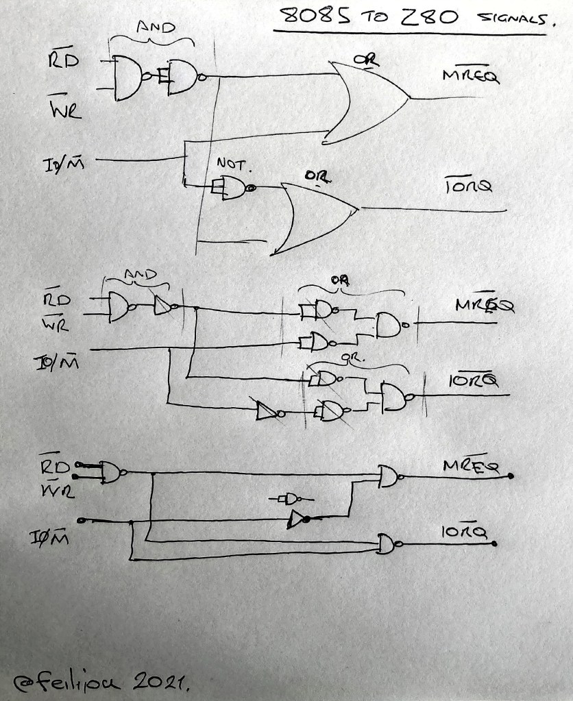
Converting 8085 signals to Z80
Other Bus Timing Issues
Several Z80 peripherals use the READY signal to cause the Z80 to wait until they are ready to read data from the bus, or to write data onto the bus. The Z80 implements one wait state whenever it uses I/O instructions, to enable slow peripherals sufficient time to signal they are not READY to proceed. The 8085 does not add in the automatic wait state, so there may not be sufficient time for them to signal the CPU to wait. There are standard circuits available to add one wait state into 8085 bus cycles.
Motorola bus peripherals use an E or Enable clock to signal that they are being addressed. For the Z80 bus, this is typically implemented by inverting the /IORQ signal. However, for the 8085 using the method above, there may be insufficient time between the E (inverted /IORQ) and stabilisation of the address.
Z80 peripherals capable of Interrupt Mode 2 use the M1 signal to determine when they should place their interrupt address (vector) on the bus. The 8085 does not generate this signal, but since the 8085 does not support IM2 mode anyway this point is probably moot.
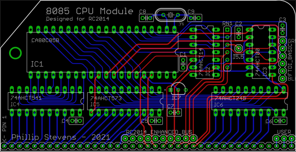
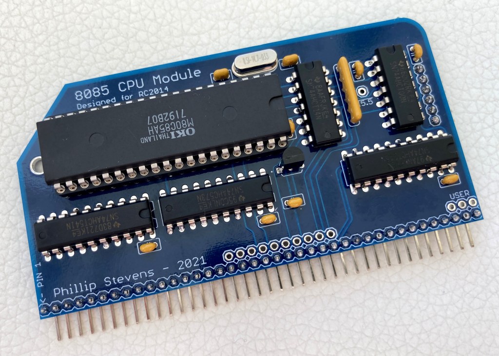
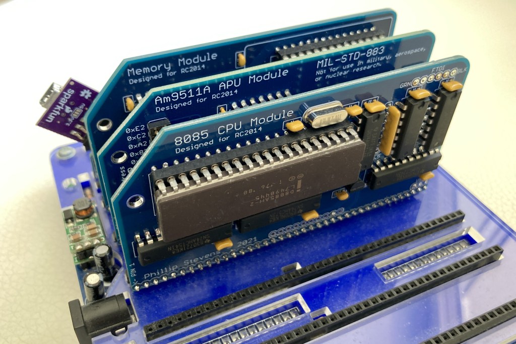
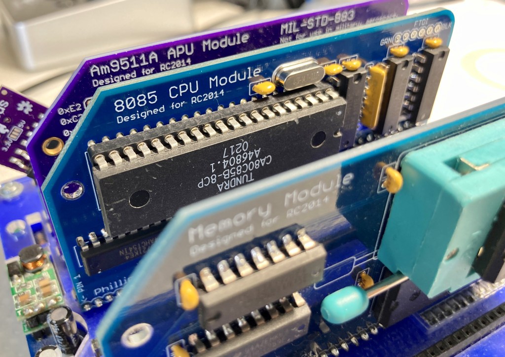
8085 CPU Module for RC2014
8085 CPU Module PCBs are available on Tindie. Combine with a Memory Module PCB to save postage.
The RC2014 Bus and Modules have been available now for some time, and the Z80 nature of the system bus provides for simplicity in the system design. There is no buffering or conversion by the CPU Module, and individual peripheral Modules are left to convert bus (or Z80) signals to suit their own requirements.
I have previously designed a few Modules for the RC2014 and, since I’ve now an interest in 8085 processors, I thought that it would be a good time to design a 8085 CPU Module.
In researching the requirements for a 8085 CPU Module to work with the RC2014 Z80 bus and standard peripheral Modules, I found the Glitchworks 8085 SBC and also Alan Cox’s 8085 designs. My initial design replicated the bus interface signalling of these two designs.
After building the first version of the 8085 CPU Module I found that the Motorola 68B50 ACIA based RC2014 Serial Module didn’t work properly. This is because on the module the required E clock is derived from Z80 /IORQ timing, and the simple method of inverting IO/M as /IORQ doesn’t provide the timing needed. The 68B50 requires the bus address to be stable before E (or /IORQ inverted) is asserted.
A second version of the 8085 CPU Module was implemented, using the above method for generating the /IORQ and /MREQ signals.
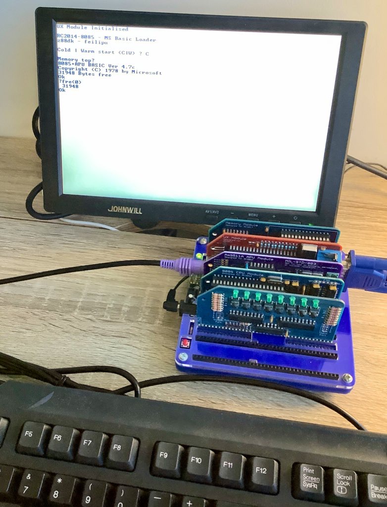
Initial tests using the modified Microsoft BASIC 4.7 for 8085 used with the RC2014 have proven to be successful. The 8085 running BASIC is marginally slower than the Z80, but it is less than 1%.
Further analysis on the performance of AHCT buffers vs unbuffered I/O to come.
Please read further for software support, including undocumented instruction discussions.
RetroChallenge 2021/10 – Am9511A APU Support
The current hardware doesn’t supply a wait state to the CPU, so the hardware interface to the APU Module designed for RC2014 doesn’t work. The 8085 CPU allows only 25ns to 30ns (depending on the manufacturer specification) for assert not READY (or /WAIT). Am9511A takes 83ns to assert /WAIT.
The retro-challenge is to extend the current 8085 CPU Module design to include a wait state generator for IO instructions to support the APU Module and the UX Module.
Retrochallenge – 1st Update – 2nd October
Getting to Am9511A APU support for the RC2014-8085 machine means firstly getting the fundamental 8085 platform working.
The RC2014 is supported by the “newlib” of Z88DK, which is meant for Z80, Z180, Z80N (Spectrum Next) processors, and the 8085 is supported by the “classic” library. So this is the first time that a newlib machine is using classic lib libraries. Confusing? Yes I find it so.
Anyway the trick is just getting the right pieces to link together. Having ZIF ROM and TL866CS Programmer helps with fast programming cycles.
Retrochallenge – 2nd Update – 3rd October
Now the z88dk RC2014-8085 ROM build using the ACIA Serial Module is working (along with the RAM build supported by Basic), I’ve spent the past days tidying the ACIA builds around my various repositories, to keep everything consistent. So now my BASIC builds for both 8085 and Z80 are aligned with RC2014 HexLoadr BASIC, CP/M-IDE ACIA, and also the z88dk ACIA newlib device code. Also took the time to clean up some the SIO device code too.
@suborb is working on the z88dk classic library crt0 and compiler intrinsics, as they’ve been stuck in both classic and newlib and are a bit disorganised. Hopefully the result will be one set that can be used for both compilers (zsdcc, and sccz80) and both libraries, across multiple machines (8080, 8085, GBZ80, Z80, Z180, Z80N, etc) which will make maintenance much easier.
Waiting now for China to come back from National Day holiday, so I can get started with new hardware.
8085 Wait State Generator
Retrochallenge – 3rd Update – 8th October
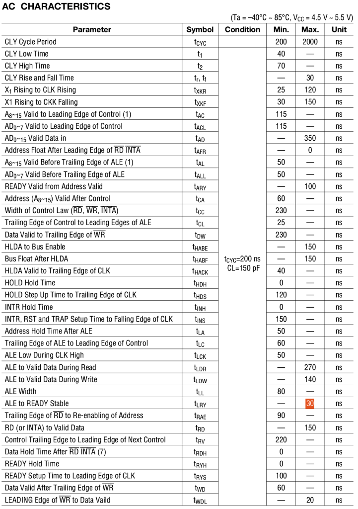
As noted above the window of opportunity for a 8085 bus peripheral to signal not READY is very short. In fact is is no more than 30ns from fall of the ALE signal, and this is 30ns before the /IORQ signal is even enabled.
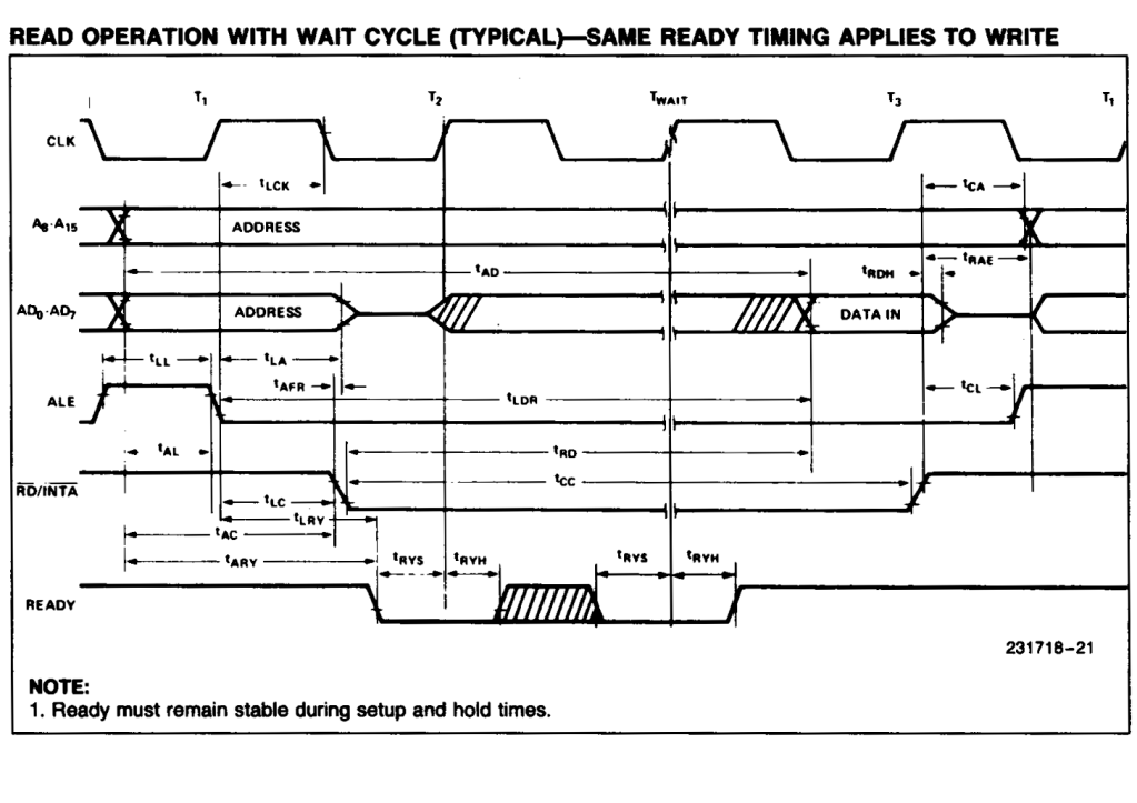
Timing information from the 8085 datasheet shows tLRY as maximum 30ns, and tLC as minimum of 60ns.
To be able to connect devices designed for the Z80 bus to the 8085 CPU we will need to implement a wait state generator. In the best case this will only affect I/O cycles, and will not slow down normal memory read and write cycles.
Designing the 8085 /IORQ Wait State Generator
As the need to generate a wait state was well known at the time of release of the 8085, several sources include the information required for the design of a basic solution. It is left to the reader to determine how to use the created wait state though.
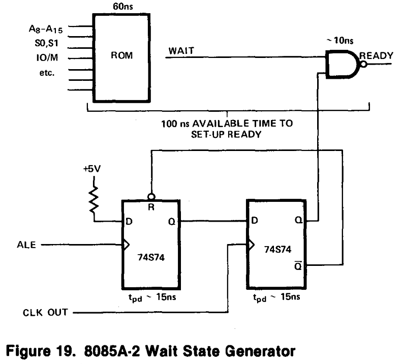
For our purposes we need to have a wait state generated only for peripheral devices, accessed using the I/O instructions. Therefore we can modify the above circuit to only generate a wait state when the I/O address space is active, or when the external Z80 bus /WAIT signal is active. The below circuit produces a /READY signal that provide 1 wait state whenever the I/O address space is active, and can continue to produce wait states until the /WAIT signal is de-asserted.
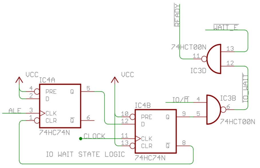
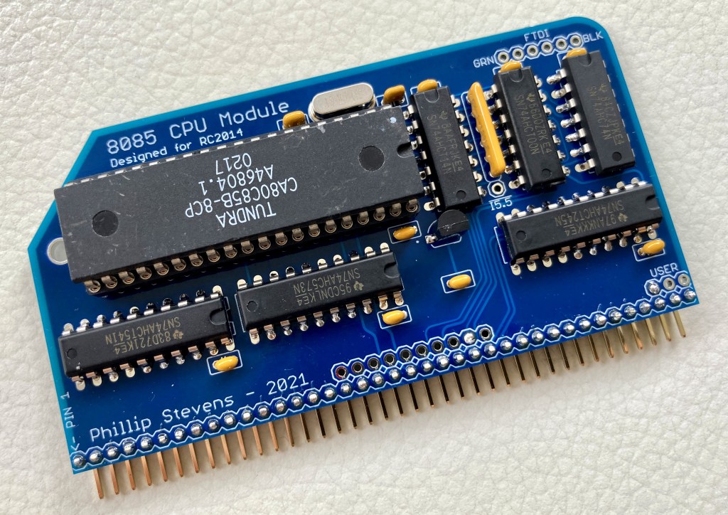
As the static RAM / EEPROM memory devices we are using are not sensitive to the timing of the /MREQ signal, the NAND gates assigned to generate a correct Z80 /MREQ have been recovered and reused in the implementation of the wait state generator. Therefore the revisions required only one additional device on the PCB. Based on this design a revised 8085 CPU Module was created, and ordered. Due to arrive around October 18th, which won’t leave much time to finish before the end of the RetroChallenge. It will be a rush, as usual.

Retrochallenge – 5th Update – 13th October
The new 8085 CPU Module PCB arrived, so wasting no time I’ve build one up to test. And it works!
It is interesting to look at the signals actually appearing on the RC2014 Bus during the operation of the APU. Here we have a floating point read from the APU, 4 bytes, where the wait state generator produces sufficient delay (1 wait state) to allow the APU to generate its own /WAIT signal for the last two bytes.
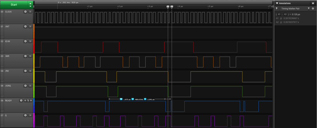
The floating point write cycle is similar but the duration of the /WAIT signal from the APU is longer, and the APU needs to assert it on every byte written. Note that tRYH is 0ns, so there is no need to hold the /READY signal beyond the clock rise point.
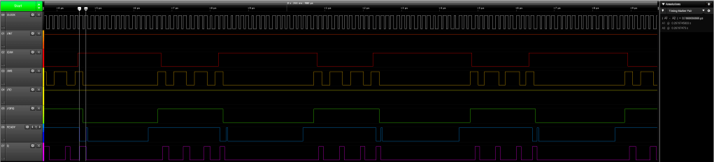
To support the Am9511A APU Module the /WAIT signal has to be patched to the USER1 Pin (if using the standard RC2014 backplane), which allows the Am9511A to extend the single wait state generated by the 8085 CPU Module for as long as the APU needs.
I’ve prepared a specific version of MS Basic 4.7 for the 8085 CPU Module when used with the Am9511A APU Module. Initial testing is working. It is looking very good to achieve the RetroChallenge goals. Please read further at the 8085 Software post for more information.
With the Wait State generator functioning, it is now possible to use the UX Module for a VGA screen and PS/2 Keyboard.
Retrochallenge – 6th (Final) Update – 26th October
Rework of z88dk classic 8080/8085/gbz80 library l_ functions.
When working with the 8085, the biggest issue is the continual pressure on the few CPU registers. Alongside the 8-bit accumulator a register and the 16-bit accumulator hl registers we have only two additional register pairs that can be used, the bc and de registers. This gives the system programmer few options but to use static memory locations to store intermediate values, which leads to non-reentrant code.
Having non-reentrant code is normally not a problem, but it does lead to issues when multiple threads (or tasks) are trying to use the CPU at the same time, for example when a multi-tasking operating system is to be supported. So it is useful to try to build reentrant functions that use the stack for storage of intermediate values, rather than static memory locations.
The designers of the 8085 had this in mind when they designed the additional functions found the 8085 silicon. The “new” instructions make it very efficient to build stack relative functions (compared to the 8080), and this relieves some pressure on the small number of registers.
However, there was one oversight made by the designers, as the 8085 af register pair cannot be used, in contrast to the z80, to pop and push arbitrary words on the stack. This reduces the number of available 16-bit registers by 1 of possible 4. There is one flag bit that always reads as 0, which is an subtle but annoying limitation of the 8085.
For the past two weeks I’ve been working on a refresh of all of the integer and long basic compiler use l_ functions to try to make them reentrant and, where possible, to optimise them for the 8085 CPU. I’ve also moved the improvements to the 8080 and Gameboy Z80 CPU where possible too.
As background, some of these functions originate from the 1980s and 1990s in the Amsterdam Compiler Kit, and haven’t been updated or improved for the past 20 years. They weren’t broken. But they were in need of some attention.
So this update is the final one in the October 2021 RetroChallenge. All the new functions are checked in and are now part of the z88dk.
8085 CPU Second Sources
Recently I purchased some second source 8085 CPUs, and an additional Intel OEM option to test. As the RC2014 System runs at 7.3728MHz, beyond the specification of most of the 8085 CPUs below, it is very gratifying that all of the selected second source CPUs function correctly, with just one exception.
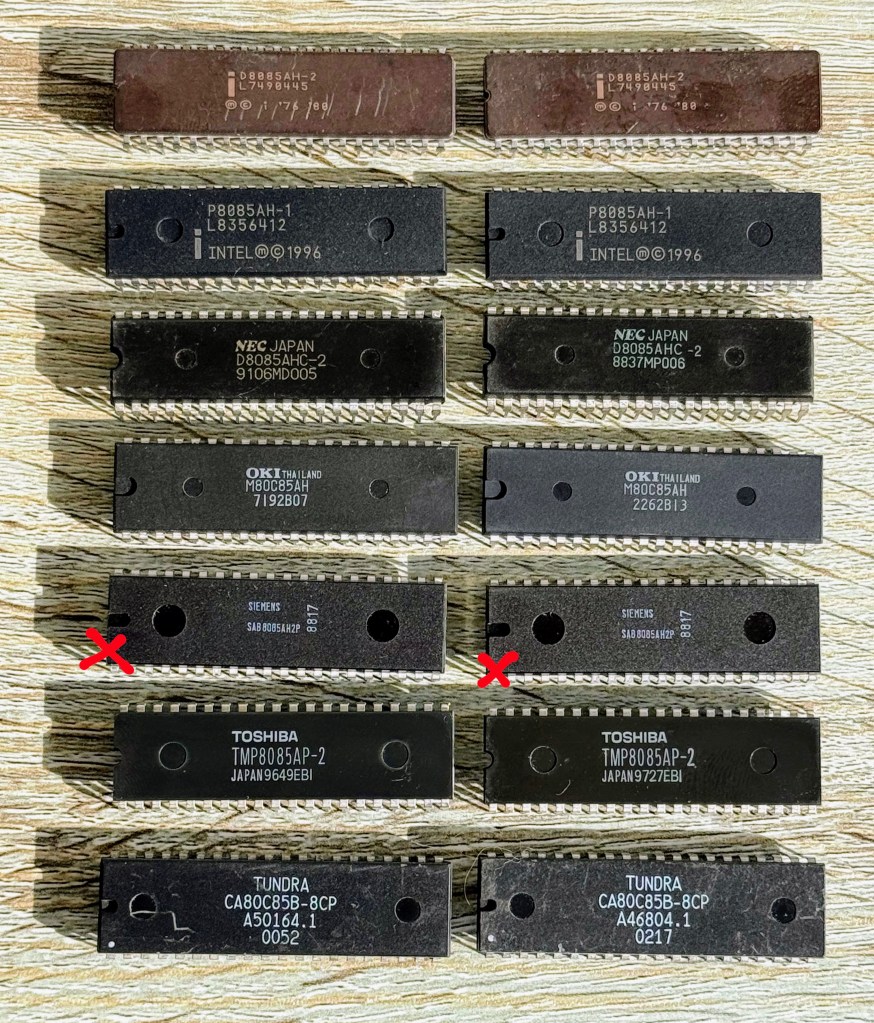
Some very simple testing was done to determine how much current each CPU implementation required, and from this it is clear which devices are implemented in NMOS, and which in CMOS. Only the OKI and Tundra devices seem to be CMOS.
Testing was done with a minimal RC2014 CP/M-IDE System consisting of a Backplane 8 equipped with an ACIA Serial Module, a CF Module Version 2, a Memory Module, and an 8085 CPU Module.
To get an approximate base line current requirement the CPU was unplugged and the remaining power requirements were measured. Two different measuring methods were used, which don’t quite align, but the relative results are quite consistent.
| Identifier | Date / Version | Freq Specification | Current 1 | Current 2 |
| Baseline | No CPU | ~ | 0.12A | 100mA |
| Intel D8085AH-2 | 1987 Week 43 | 5MHz | 0.11A + Baseline | 79mA + Baseline |
| Intel P8085AH-1 | 1996 | 6MHz | 0.07A + Baseline | 69mA + Baseline |
| NEC D8085AHC-2 | 1988 Week 37 | 5MHz | 0.07A + Baseline | 81mA + Baseline |
| OKI M80C85AH | 5MHz | 0.01A + Baseline | 15mA + Baseline | |
| Siemens SAB8085AH2-P | 1988 Week 17 | 5MHz | Failed | Failed |
| Toshiba TMP8085AP-2 | 1997 Week 27 | 5MHz | 0.07A + Baseline | 79mA + Baseline |
| Tundra CA80C85-8CP | 2002 Week 17 | 8MHz | 0.01A + Baseline | 10mA + Baseline |
Personally, I keep both Intel CPUs in my 8085 CPU Modules. The original ’76-’80 ceramic D8085AH-2 looks good paired with a similar vintage Intel 8231 APU. As a daily usage system, the 1996 release (20 years more recent) P8085AH-1 is specified to 6MHz and is (with the exception of the modern CMOS Tundra device) the closest specification to the RC2014 CPU Frequency. But realistically it makes no difference which one you use.

Pingback: Adding an 8085 CPU on a Z80 Bus for the RC2014 computer @_feilipu @ZxSpectROM « Adafruit Industries – Makers, hackers, artists, designers and engineers!
Pingback: CP/M-IDE for RC2014 | feilipu