There has been quite bit of interest in assembly or machine monitors for the RC2014 lately, so I’ve taken the opportunity to write one in MS (NASCOM) BASIC which will work for RC2014 Mini / Micro / Classic ][ machines, but equally well for any machine running a version of MS Basic 4.7 or later.
The functional goal was to provide the same user tools as the NASBUG monitor, but to be maintainable and easily customisable by the user. As the monitor is written in BASIC it works equally well for both Z80 based RC2014 machines and 8085 based RC2014 machines using my 8085 CPU Module (for example).
A key issue for me was that it needed to fit completely into the BASIC program memory found below the default z88dk assembly loading address of 0x9000 for the RC2014 target.
By using BASIC language for the monitor it enabled me to focus on the functionality, as BASIC provided the command line support via INPUT(), string tokenisation via MID$(), ASC(), and VAL(), and mathematical functions.
However, Fred W. has provided a better simpler solution for getting an integer from a hexadecimal string and now that solution has been implemented.
With that key function done, then the MID$() function was used to tokenise the command string into 4 (or less) digit strings to convert into hexadecimal. Depending on the function required either signed integers were then produced to be an address or where a length was needed an unsigned integer was provided.
Finally an IF THEN tree was made to process the command string, found using the very convenient ASC() function. Since the commands are sparse, I thought that a simple decision tree would be best.
As noted, a key goal for me was that it needed to fit completely into the BASIC program memory found below the default assembly loading address 0x9000. The program fits with over 100 Bytes free, currently. But the stripped version has still over 1200 Bytes free, so there is quite a lot more code that could be added if needed.
Program Usage
The BASIC monitor is useful to casually poke around in the RAM or ROM of a running MS BASIC RC2014 machine to get a feeling of how variables and strings are stored, for example.
It can be used to enter assembled binary code into the RAM, and then run it. The assembly code can use the facilities (serial I/O, RST table, and MS Basic functions) as needed. Some further information on Assembly can be found here.
Further, it can be used together with the Zen Editor/Assembler to write and then assemble larger programs for the RC2014. When the monitor is used together with Zen, the monitor can be loaded (copy / pasted) into the BASIC Command Line, then using the BASIC HLOAD command Zen can be loaded (cat) into the RAM at 0x9000, and launched either from the monitor or directly using ?USR(0). Once editing and assembly is finished, Zen can be exited with Q and then the newly assembled program can be run from its origin by entering the monitor with run, and then E xxxx yy, where yy is a signed integer input parameter.
Using this combination of Zen and the BASIC monitor it is possible to develop, examine, and modify complex Z80 and 8085 assembly code in a very comfortable environment.
Commands for a BASIC Monitor (Syntax borrowed from NASBUG)
A – hexadecimal arithmetic
A xxxx yyyy – Responds with: SSSS DDDD JR JJ. SSSS is sum of xxxx and yyyy. Values in Hexadecimal. DDDD is difference of xxxx and yyyy, yyyy-xxxx. Values in Hexadecimal. JJ is displacement required in a Jump Relative instruction which starts at xxxx, to cause a jump to yyyy. Value in Decimal.
C – copy
C xxxx yyyy zzzz Copy a block of length zzzz from xxxx to yyyy. One byte is copied at a time, starting with the first byte, so if there is an overlap in the two areas data may be destroyed. This command is useful for filling a block with a single value. Make yyyy one greater than xxxx and put the required value into address xxxx using M. Set zzzz to the number of bytes required. Values in Hexadecimal.
E – execute
E xxxx yy – Execute program at xxxx, supplying integer input parameter yy. The USRLOC location depends on the specific MS BASIC ROM implemented. The value can be easily adjusted in the monitor source code. Values in Hexadecimal.
I – intelligent copy
I xxxx yyyy zzzz – Like the Copy command but copies to ensure it will not cause data corruption in an overlapping section. Values in Hexadecimal.
M – modify store
M xxxx – Modify memory starting at address xxxx. The address is displayed followed by the current data. The data value may then be changed. Continuous entry of new data values is supported. Values in Hexadecimal.
Q – quit
Q – Quit to BASIC Immediate Mode (Command Line).
T – tabulate
T xxxx yy – Tabulate (display) a block of memory starting at xxxx and continuing to yy-1. Values in Hexadecimal.
Further Development
As the monitor is written in BASIC it is easy to maintain for all hardware or CPU types wherever MS BASIC is found, and to further develop to support new functions. As there are about 1200 Bytes free below the default origin (in the stripped version), there is space for the user to add their own preferred functions or modifications to existing functions.
ReGIS graphics can be used to build high quality vector graphical output for embedded (Serial) devices, for example Arduino devices or retro-computers such as the RC2014 running CP/M, with the graphics output being displayed on a Windows 10 desktop. This method uses WSL Ubuntu with XTerm to support graphical output for Serial connected embedded devices, and a Windows based X Server to host the display.
Background
From the Wikipedia, ReGIS, short for Remote Graphic Instruction Set, is a vector graphics markup language developed by Digital Equipment Corporation (DEC) for later models of their famous VT series of computer terminals. ReGIS supports vector graphics consisting of lines, circular arcs, and similar shapes. VT series terminals supporting ReGIS generally allow graphics and text to be mixed on-screen, which makes construction of graphs and charts relatively easy.
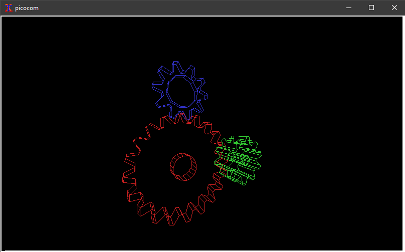
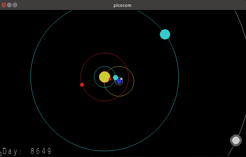
ReGIS is useful to display information that can be more easily interpreted as a diagram or a graph, such as plotting planet motion. It can also be used for vector graphics such as the GLX Gears program.
Today, where DEC VT series terminals are impractical to obtain, the easiest method to display ReGIS vector graphics is to use the XTerm terminal emulator. The XTerm fully supports ReGIS, but this capability is not enabled in general release versions. We’ll need to compile our own version with ReGIS enabled.
XTerm was developed for the X Windows System running on versions of Unix or Linux. So to use it on a Linux desktop machine running (e.g. Ubuntu) is quite straightforward. But if we want to use it on a Windows 10 desktop we will need to jump through some additional hoops and that is the point of this story.
The X window system (X) is a client / server windowing system developed in the mid 1980’s to support remote windowing. Unlike most earlier display protocols, X was specifically designed to be used over network connections rather than on an integral or attached display device. X features network transparency, which means an X client program running on a computer somewhere on a network can display its user interface (window) on an X Server running on some other computer on the network. The X Server is typically the provider of graphics resources and keyboard/mouse events to X clients, meaning that the X Server is usually running on the computer in front of a human user, while the X client applications run anywhere on the network and communicate with the user’s computer to request the rendering of graphics content and receive events from input devices including keyboards and mice.
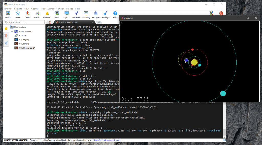
To get XTerm to connect to a Serial interface, provided by an Arduino device or by a retro-computer such as a RC2014 CP/M machine, it is necessary to use a dumb terminal emulator to pipe the Serial bit-stream originating on the Serial-USB (FTDI) interface connection to XTerm without tampering with the non-displayable ESC code sequences that ReGIS uses for signalling. The best option is to use picocom for this role. Most other terminals “cook” the Serial to remove those ascii control characters that can’t be displayed, rather than passing them transparently.
We now have a complete solution to display ReGIS graphics originated on an Arduino or RC2014 on Unix / Linux machines. XTerm, configured with ReGIS enabled, together with picocom to pipe the Serial bit-stream is all that is required to display vector graphics on a Linux desktop.
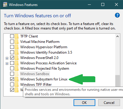
To use Windows 10 as the desktop we will need to host a Unix / Linux machine running XTerm and picocom somewhere connected to the embedded device, and provide an X Server on the Windows 10 machine to display the window generated by XTerm. This can be done with a completely separate Linux machine, such as a Raspberry Pi or similar, but it is more convenient to do it using a Virtual Machine inside the Windows 10 platform provided by Windows Subsystem for Linux.
Microsoft provides two versions of the WSL. The first version WSL1 uses specific services and drivers to give Linux applications access to the Windows 10 kernel and file system. WSL1 supports access to Serial interfaces and the host file system. The use of the specific services and drivers between the Windows 10 kernel and Linux causes a performance penalty for most Linux applications, so WSL2 was introduced with a lightweight virtual machine, based on Hyper-V, to optimise Linux application performance. However WSL2 does not allow access to Serial interfaces or direct access to the Windows 10 file system. For most applications WSL2 is a better choice, but as we need to access the Serial interfaces directly we need to use WSL1.
With WSL1 installed, we can create an Ubuntu 22.04 LTS based Linux system to install and host our XTerm and picocom applications. And, optionally, we can build z88dk following these instructions, and install z88dk-libraries supporting ReGIS providing a C interface for RC2014 CP/M applications.
From our Windows 10 desktop machine we need to provide an X Server to enable XTerm to display its window on our desktop. There are several options available to do this. Xming (not free) and VcXsrv (open source) are two that are commonly recommended.
Another option to provide a Windows 10 X Server is MobaXterm. MobaXterm is proprietary, but is available for free for home users. It provides both an X Server (based on X.org) and secure shell (SSH) capability. SSH is particularly required where we need to connect to XTerm and picocom (the X client) running on separate Raspberry Pi hardware, but it is also useful for Windows 10 WSL. However, we can access WSL Ubuntu directly through its own terminal to initialize the XTerminal session, so for WSL Ubuntu the SSH capability is just a very convenient “nice-to-have”.
Implementation
Lets go through the steps required to get this all working…
Windows Subsystem for Linux & Ubuntu
The Windows Subsystem for Linux (WSL) allows Linux / Unix distributions to use the Windows host computer. This instruction is based on Ubuntu 22.04 LTS, but other distributions will be similar.
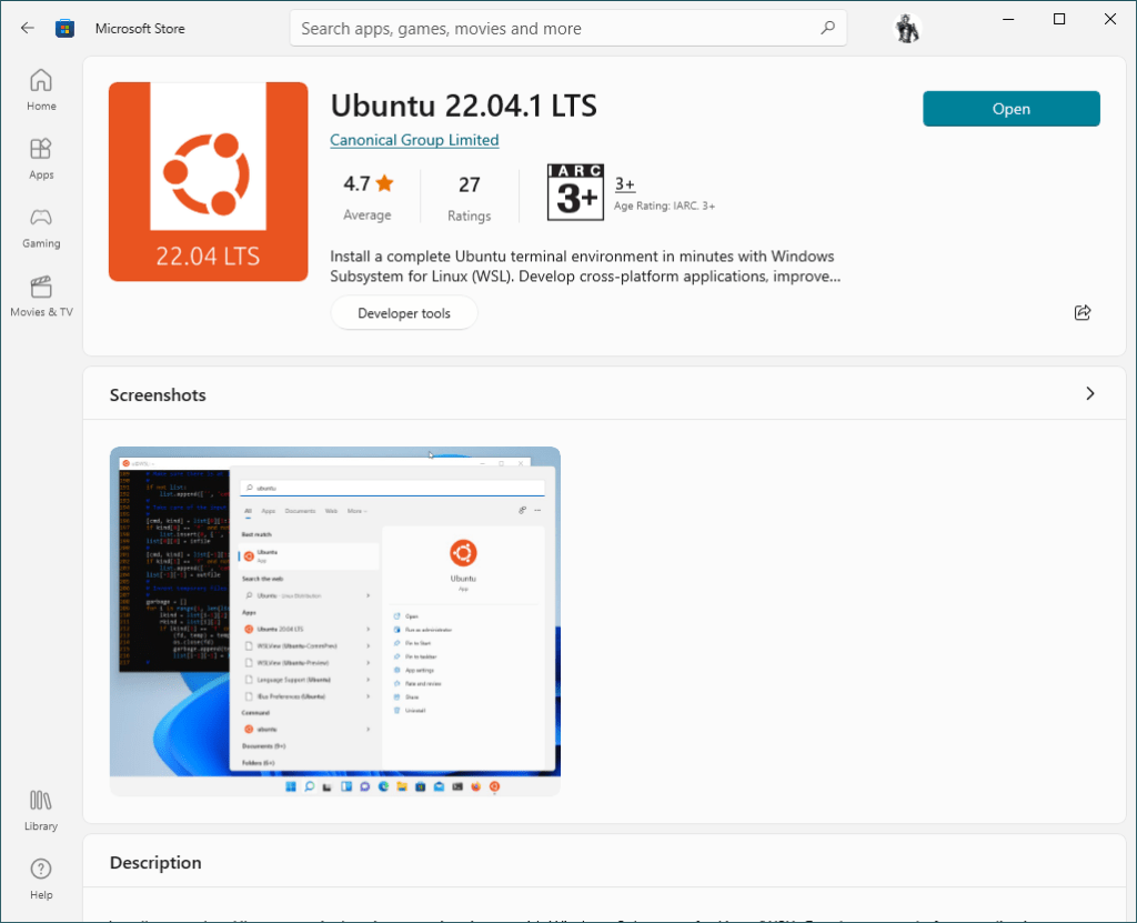
Once WSL is installed then go to the Microsoft store and install Ubuntu 22.04 LTS. There are options for both Windows 10 and Windows 11, so choose the suitable alternative.
Ubuntu 22.04 LTS for WSL installed from the Windows Store.
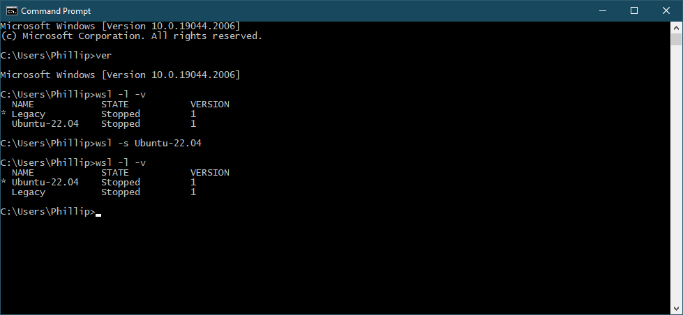
Confirm that you have both WSL1 and Ubuntu 22.04 LTS installed using. > wsl -l -v
And then set the default distribution to Ubuntu-22.04. > wsl -s Ubuntu-22.04
Setting the WSL version and Linux distribution.
Then launch the Ubuntu 22.04 LTS subsystem using the Windows Start menu command, to configure the new distribution. Update and upgrade the packages using apt, and make any other adjustments you need. Set up directories that you will use to build XTerm and (optionally) build z88dk. Building z88dk will ensure that you have the prerequisites to prepare .COM files for later uploading to your RC2014 CP/M.
At this stage DO NOT install XTerm or picocom from the Ubuntu repositories.
Launch the installer. It will automatically recognise your installed WSL and Ubuntu 22.04 LTS instances and will automatically configure SSH (local) terminal access for them. It will also allow you to connect directly to your Serial attached Arduino or RC2014 retro-computer if you configure a serial connection.
Use MobaXterm to connect to your Ubuntu 22.04 installation. The advantage of doing this is that the DISPLAY environment variable is automatically set, so that later XTerm can find the Windows 10 screen with no further setting needed. However, the direct Ubuntu 22.04 terminal can alternatively be used later for other purposes with no problem.
Preparing XTerm to support ReGIS
XTerm is the only known software solution supporting ReGIS. But it doesn’t support ReGIS in the default build. You’ll need to enable ReGIS support yourself by building and installing a customised version.
From your WSL Ubuntu command line use the below recipe. If you have not built any prior code on your WSL Ubuntu installation you may need to add additional packages, as signalled by the configuration step. Use apt to install them as needed.
> sudo apt install -y build-essential libxaw7-dev libncurses-dev libxft-dev
> wget https://invisible-island.net/datafiles/release/xterm.tar.gz
> tar xf xterm.tar.gz
> cd xterm-373
> ./configure --enable-regis-graphics
> make
> sudo make install
Install picocom for Ubuntu 18.04 LTS
From Release Version 3.0 picocom implemented advanced terminal control system calls, which are unsupported by the Windows 10 WSL1 implementation. This means that the Ubuntu 22.04 LTS supported release for picocom can’t be used with WSL1.
To work around this problem the Ubuntu 18.04 LTS Release Version 2.2 of picocom for amd64 can be installed. From your Ubuntu terminal, download the picocom 2.2-2 package and install it using dpkg.
Once it is installed, it is also useful to install the lrzsz package which provides XMODEM capability for picocom and other terminals.
It is also useful to hold the picocom package to ensure that it is not automatically upgraded to a later (unusable for our purpose) version. That is done with apt-mark.
To initialise XTerm for VT340 emulation, connecting to Windows 10 Serial device COMx, from the MobaXterm terminal use this command string. This command assumes we’re using 115200 baud 8n2 with RTS flow control, and we’re going to use XMODEM protocol to send binaries to our RC2014 or other device. Check the picocom manual to adjust the serial interface configuration to your own needs.
At this point a new XTerm window should appear on the Windows 10 desktop, supported by the MobaXterm X Server.
Assuming that you have a program which can generate ReGIS graphics already installed on your RC2014 (or Arduino), such as the demo program provided here, then it is time to start the program from the CP/M command prompt. Otherwise, it makes sense to use XTerm (with picocom) to access your RC2014 and upload the provided ReGIS demo program, or other any other program, using XMODEM protocol and the XM.COM or XMODEM.COM program on your CP/M installation, and then launch the program from the CP/M command prompt.
The resulting XTerm window (example image shown is planet-motion) should look similar to the image below.
Windows 10 with XTerm window displaying planet-motion.
And that is then all that needs to be done to enjoy high resolution vector graphics generated by a Serial connected embedded device such as an RC2014 running CP/M or an Arduino device.
The ReGIS library for z88dk has been developed to support ReGIS on the RC2014 and other Z80 CP/M machines. Therefore programs can easily generate the required Serial codes using the C functions provided.
The ReGIS library for Arduino is hardware agnostic, and supports all Arduino architectures. It can be installed from the Arduino Library Manager.
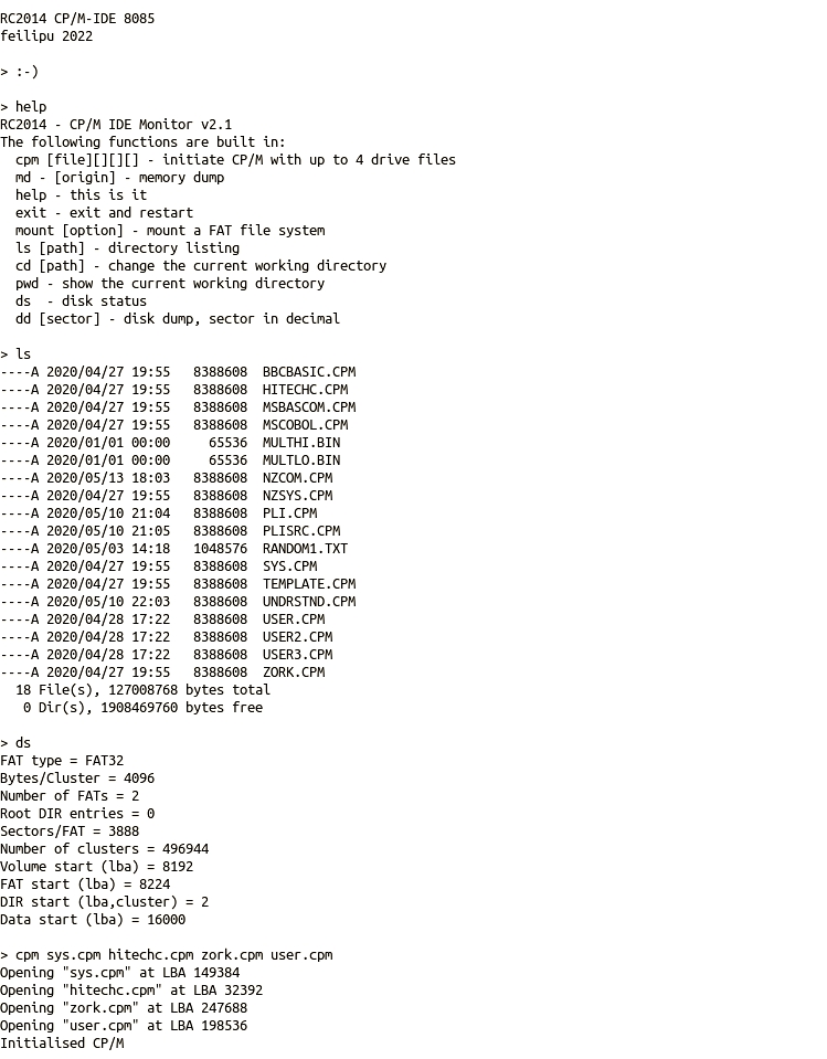
Just over 4 years ago, on 18th March 2018, I committed the first CP/M-IDE files into the RC2014 repository. Now that some time has passed and it has developed into a stable solution for CP/M I think it is time to fill in some details about why it was written, how it differs from other CP/M implementations, and how to reproduce images to match those in the CP/M-IDE repository.
Concept
There are several implementations of CP/M available for the RC2014. Initially, the CP/M on a Breadboard project implemented by Grant Searle became the default implementation for the Z80 RC2014. Slightly later Wayne Warthen added support for the RC2014 to the Z80/Z180 RomWBW System. RomWBW is a very extensive and advanced set of system software, supporting many different RetroBrew machines, and in general it requires 512kB ROM and 512kB RAM to reach its full potential.
Each of these implementations has its own focus. The 9 Chip CP/M is based on simplicity, and being able to be built on a breadboard with the minimum of complexity, but it has not been maintained (e.g. correcting the bugs in the SIO and ACIA serial implementations requiring arbitrary interstitial delays to be inserted, otherwise data loss occurs) and it has a substantially smaller TPA. Alternatively, RomWBW supports a variety of hardware including Z180 CPUs, and provides an underlying generalised architecture support which provides paged memory and many facilities but this imposes a processing overhead on I/O, and requires substantially more RAM (512kB) than a typical CP/M system.
Faced with both these options, and being very interested to build my own solution, and to use my growing experiences supporting the z88dk community, I decided to build CP/M-IDE to fulfil a specific niche.
The CP/M-IDE is designed to provide support for CP/M on Z80 while using a normal FATFS formatted PATA or IDE drive. And further, to do so with the minimum of cards, complexity, and expense. Most recently, it has also become the CP/M which supports the 8085 CPU Module. Also recently, support for the standard RC2014 Pro with CF Module v2.1 and for the RC2014 Mini II with CP/M Expansion Kit has been added.
Initially I chose the IDE Hard Drive Module specifically because I could use it to attach any old hard drive, aka “spinning rust”, to my RC2014, and this led to support for everything from these old 3 1/2″ hard drives, through to modern SSD or DOM solid state drives. It also supports both old and modern high capacity Compact Flash Cards in their native 16-bit mode, so readily available modern 1 and 2 GigaByte Compact Flash cards are OK. It is also possible to use SD Card to CF Card adapters with the IDE Hard Drive Module or the CF Module v2.1, allowing direct support of modern pluggable SD or Micro SD storage.
I also wanted to build a very inexpensive system so the original RC2014 Pro with CF Module v2.0, or RC2014 Mini with CP/M Expansion Kit, is sufficient for modern storage solutions. And as an option the RC2014 IDE Hard Drive Module is the only additional Module required to operate CP/M-IDE with older “spinning rust” hard drives. It is NOT necessary to buy an expensive 512kB/512kB Memory Module as the standard 64kB RAM Memory Module works fine. If there’s no need or interest to attach proper IDE hard drives, or using a Compact Flash Module for storing CP/M drives is preferred, then there is no additional hardware required over the RC2014 Pro standard product.
CP/M is a very compact Operating System and, in the most common version 2.2, it supports only serial interfaces and disk interfaces. For the RC2014 there are two standard serial Modules, being the ACIA Module (used in the RC2014 Mini) and the more advanced and expensive SIO/2 Module (used in the RC2014 Pro).
As I’m quite interested in building real-time and event driven systems, in contrast to other CP/M implementations, CP/M-IDE therefore includes drivers supporting both transmit and receive interrupt based solutions, sourced from my z88dk RC2014 support package for the ACIA serial interface and the SIO/2 serial interface.
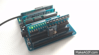
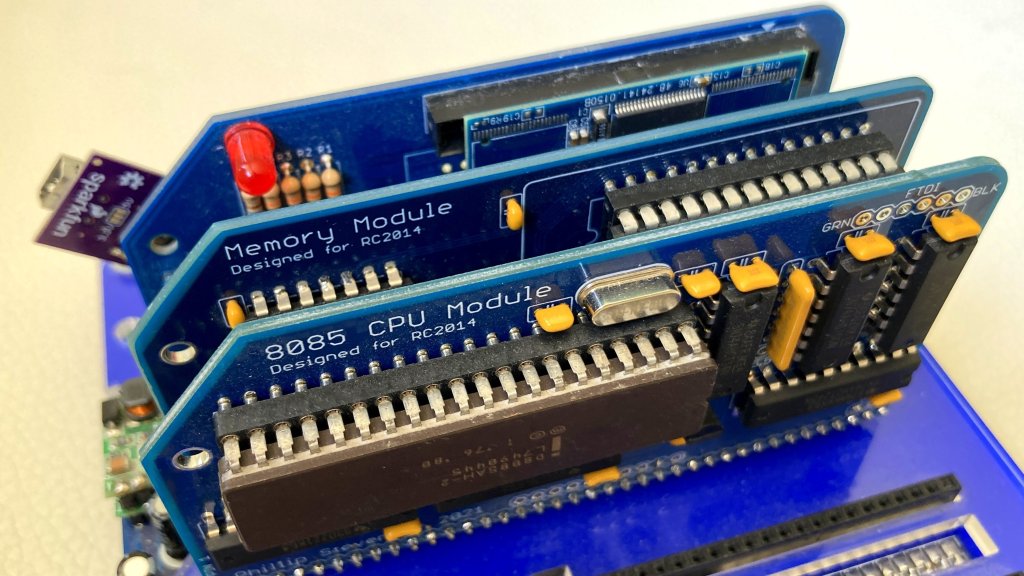
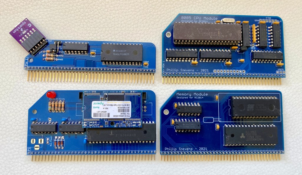
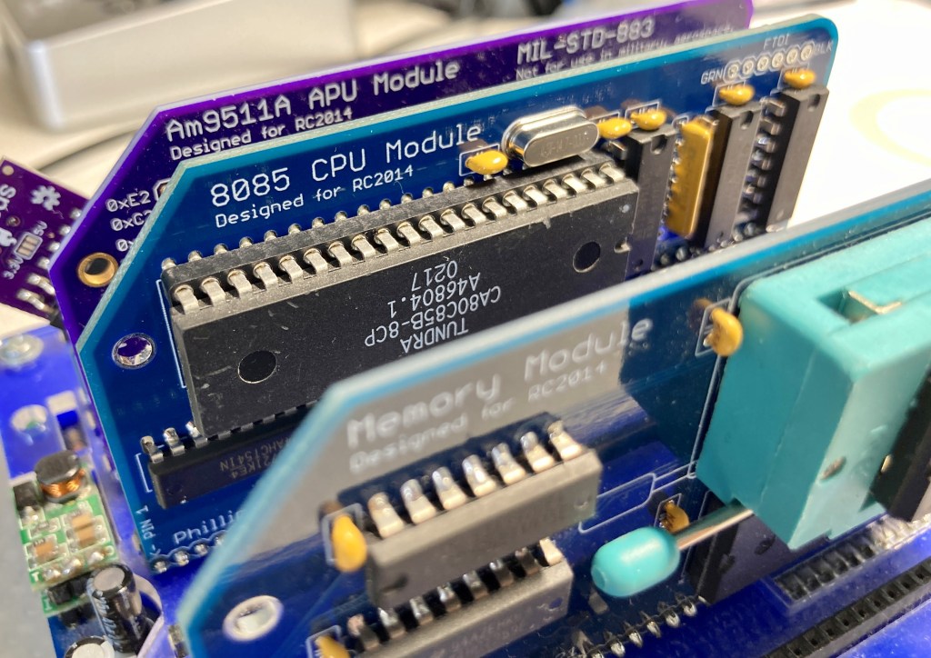
8085 CPU Module
More recently I have built a 8085 CPU Module for the RC2014 System. This is the first time that an 8085 CPU has been integrated into the RC2014 System, and it is able to work with the Z80 bus signalling required to drive the standard RC2014 Modules.
CP/M-IDE 8085 RC2014 System
I am very pleased to have a wholly Intel RC2014 System equipped with the 8085 CPU Module, the 8231A APU Module, and the 8255 IDE Module. This is the original “Intel Inside”, before it became marketing jargon.
Hardware
The concept remains to use the minimum of additional hardware over the entry level RC2014 Pro model. In fact just the IDE Hard Drive Module is desirable. But, the standard CF Module v2.0 (and derivatives) can also be used as it supports modern (large capacity) CF Cards, and the RC2014 Classic II with CP/M Expansion Kit is also supported.
IDE Hard Drive Interface
The IDE Hard Drive Module is based on the 8255 PPI device. This device was designed to work with the 8085 CPU and 8086 CPU. It is perfectly suited to supporting a 16-bit parallel IDE interface as it provides latching of signals on 3 separate 8-bit ports.
Initially I was concerned that the selection of control signal pins for the IDE interface limited the possibility for use of the 82C55 device for generalised I/O. I still think that this is an issue but, since no one has implemented further generalised solutions, the point is moot.
The IDE Hard Drive Module supports PATA hard drives of all types (including SSD IDE and DOM storage) and Compact Flash Cards and SD Card Adapters in native 16-bit PATA mode with buffered I/O being provided by the 82C55 device.
The IDE interface (or also termed diskio) is optimised for performance and can achieve over 110kB/s throughput using the FatFS library in C. It does this by minimising error management and streamlining read and write routines. The assumption is that modern IDE drives have their own error management and if there are errors from the IDE interface, then there are bigger issues at stake.
The CF Module interface can achieve over 200kB/s throughput at FATFS level, and seems to provide best performance using SD Cards in SD Card to CF Card Adapters. The old default RC2014 CF Module v1.3 is often unstable with modern CF Cards or with SD to CF Card Adapters. However the recent RC2014 CF Module v2.1 has become quite reliable with all modern large and small CF Cards. If you experience problems, then seek out this recent implementation.
For both IDE interfaces, within CP/M performance is approximately half the FATFS performance because the CP/M deblocking algorithm implements a double buffer copy process where 512 Byte physical sectors found on IDE disks are converted into the 128 Byte logical disk blocks that CP/M expects.
Serial Interfaces
In the ACIA builds, the receive interface has a 255 byte software buffer, together with an optimised buffer management supporting the 68C50 ACIA receive double buffer. The choice of memory size for the receive buffer is based on optimisations available by having the buffer a full “page”. Also text can be “pasted” in fairly large chunks into the CP/M command line without losing bytes.
Hardware (RTS) flow control of the ACIA is provided. The ACIA transmit interface is also buffered, with direct cut-through when the 31 byte software buffer is empty, to ensure that the CPU is not held in wait state during serial transmission. The size of the transmit interface buffer is based on free memory within the CP/M BIOS. As BIOS memory is typically reserved to start on the 256 Byte page boundary, if an update needed to consume more RAM, I would reduce the size of the transmit buffer to avoid the need to consume an additional page of BIOS memory.
In the SIO/2 build, both ports are enabled. Both ports have a 127 byte software receive buffer supporting the SIO/2 receive quad hardware buffer, and a 15 byte software transmit buffer. The transmit function has direct cut-through when the software buffer is empty. Hardware (RTS) flow control of the SIO/2 is provided. Full IM2 interrupt vector steering is implemented.
As both ACIA and SIO/2 devices have a hardware buffer for received bytes, it is important for the receiving interrupt handler to drain these buffers completely before returning execution to the program. If this is not done there is a danger that received bytes could be overrun and lost.
For the CP/M-IDE 8085 build the Serial Output (SOD) FTDI interface found on the 8085 CPU Module is enabled as the CP/M LPT: interface. This is activated by using ^p as per normal practice.
Additional Hardware
Whilst there is no support for additional hardware within CP/M itself (as there are no BDOS calls standardised), it is possible to use additional hardware in CP/M applications. Typical hardware options include the APU Module, various Sound Modules, and digital I/O Module.
CP/M Implementation
There are many descriptions of Digital Research CP/M, so I won’t go into detail. It is important to know that CP/M v2.2 was in its day the most widely deployed Operating System for small computers based on the 8080, 8085, and Z80 CPUs. Later versions of CP/M supported the 8086, and 68000 CPUs, as well as providing many more system functions than the CP/M v2.2.
Whilst there have been later versions of CP/M produced, to my knowledge, there were no widely available user applications produced which could not be run on CP/M v2.2. This broad compatibility is why CP/M v2.2 is important.
CP/M v2.2 is essentially just 4 pieces of code. The BIOS (Basic Input Output System) is provided to abstract the hardware devices from the operating system. Essentially there is a limited set of BIOS commands that the BDOS can call on. These BIOS commands are implemented specifically for the characteristics each machine, and in the early days of computing it was essential that a user knew how to write their own BIOS.
The second piece of code is the Page 0 of memory, which is written by the BIOS cold boot command on initialisation. The role of this Page 0 is to provide important addresses (for both BIOS and BDOS) and to set important status registers like the I/O Byte. The Page 0 is also used to manage the 8080, 8085, and Z80 CPU interrupt vectors, and to store the command line entered by the user when an application is initialised.
The CP/M BDOS is the middle layer of the Operating System. Application programs rely on BDOS system calls to support their requirements. Here the drives (A:, B:, through to maximally P:) are opened and closed, and disk sectors are written. The BDOS does its work by calling BIOS commands on behalf of the application that is currently loaded.
Often the BDOS is combined with the CCP (Console Command Processor) into one assembly language file because both of these components are constant and they are independent of the hardware. These two components are essentially the distribution of Digital Research CP/M which was sold to the user.
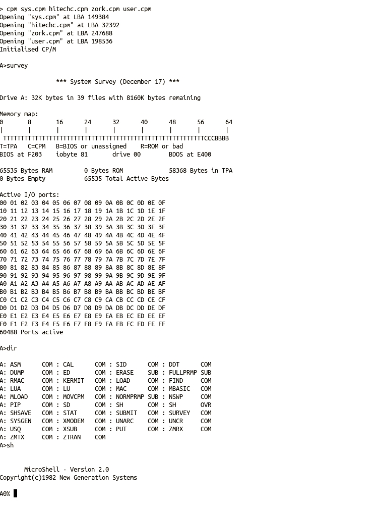
The CCP is the user interface for CP/M. It provides a very small number of integrated commands, like “directory list”, “erase”, “rename”, “type” or “exit”, but its main role is to load additional commands or applications called “Transient Programs” into RAM and execute them. Often, an application loaded into the Transient Program Area (TPA) RAM will overwrite the CCP in memory as it is normal for the CCP (and BDOS) to be reloaded once an application quits.
There are third-party alternatives available for both the CCP and BDOS, and as these are loaded each time the computer is restarted it is possible to replace the default versions by alternatives if desired. Specifically for CP/M-IDE, the DRI CCP can be replaced by Microshell SH (here), or both CCP and BDOS can be replaced by NZCOM also known as Z System without impacting the installed ROM system components.
CP/M Drives
CP/M was developed before there was a standard implemented for computer disk drives, and every system had its own peculiarities. In order to cope with this situation each BIOS had to be written to cover the possibilities, by completing a Disk Parameter Block. Each disk type needs its own DPB, which takes space in BIOS RAM, so it made sense for CP/M-IDE to be implemented with only one type of disk supported. Additionally each drive attached by the BIOS requires a substantial Allocation Vector RAM reservation. It needs to be said that providing for unused drives in CP/M substantially increases the BIOS size, and commensurately reduces the TPA RAM for user applications and in turn their working RAM. For comparison, CP/M-IDE has 3kB more TPA RAM available for user applications than the default RC2014 CP/M implementation.
A subtle but important advantage to using only one disk type is that every disk is orthogonal, and it can be located anywhere on the underlying physical disk (ie. starting at any LBA). Also, it does not matter into which CP/M drive A:, B:, C:, or D: a disk is mounted when booting. The CP/M “system disk” looks exactly like any other disk, and every CP/M disk file can be located anywhere on the FATFS parent drive.
Further, the CP/M-IDE CCP/BDOS/BIOS operating system binaries are loaded from ROM. This is not typical, as most CP/M BIOS implementations will load the CCP/BDOS/BIOS from the first sectors (or tracks) of the first attached physical drive, and will require the system disk to be located in specific sectors of the physical drive, and they also rely on a specific allocation of LBA addressed sectors (or slices) for all additional drives.
The CP/M-IDE system supports a maximum of 4 active drives of nominally 8 MByte each. The maximum possible size of any CP/M disk is 8 MByte, due to overflow of a 16-bit calculation within the BDOS. Further each CP/M disk can support up to 2048 files as a maximum. By setting the standard CP/M-IDE disk type to be maximised both in terms of size and number of supported files there is no question of the disk storage being too small. The only limitation introduced is that up to a maximum of 4 CP/M drives can be active at any one time, which leaves us with the maximum free TPA RAM.
The choice of 4 drives for CP/M-IDE was based on nominally having 1 drive for CP/M system utilities, 1 drive for application files, 1 drive for user data or source files, and 1 drive for temporary files. In practice I’ve found that working with 2 or 3 drives is the most common scenario, and often it makes sense to copy the few needed system utilities onto a working drive and work off that one drive.
CP/M-IDE is like having a 4 “floppy” drive machine (with 8MB floppy disks), and a library of up to thousands of floppy disks to choose from. Just insert the floppy disks you want to use when you want to use them. This interchangeable disk strategy is different to other RC2014 CP/M implementations that put everything into a maximum of 16 “hard” drives, at fixed LBA locations or slices, and leave them attached permanently.
It should be emphasised that a CP/M-IDE disk is purely a normal file from the perspective of an IDE FAT32 (or FAT16) formatted disk. It can be copied, moved, compressed (or zipped), or archived by any disk tools, in any modern O/S, as desired.
As CP/M-IDE uses LBA addressing there can be as many CP/M disks stored on the IDE FAT32 (or FAT16) formatted disk as desired, and CP/M-IDE can be started with any 4 of them in any drive. Note that CP/M does not know about or care about the FAT file system. On launch the CP/M-IDE BIOS is provided with an initialisation LBA for each of its 4 drives by the boot shell, and all future sector references to each disk (file) are calculated from these initial LBAs as provided for each drive.
As the FAT32 format supports over 65,000 files in the root directory, and a similar number of files in each sub-directory, collections of hundreds or even thousands of CP/M disk files can be stored in any number of sub-directories on the FAT32 parent disk. Knock yourself out by storing every conceivable CP/M application on thousands of disks on a single 120 GByte drive. As the CP/M Operating System doesn’t store state (the CCP/BDOS is reloaded each time an application terminates), changing or reordering drives is as simple as typing exit, and then restarting with the new drives desired using following shell command: cpm filefor.A filefor.B filefor.C filefor.D
CP/M Disks
As we can store literally thousands of CP/M disks on one FAT32 parent disk, let’s think about how to create CP/M disks, and how to store information on them. There are two main methods for building CP/M disks, being from within CP/M using native tools such as the yash shell, and alternatively from a Linux or Windows PC host with the physical FAT32 disk temporarily attached to the host. For creating, building, and organising many CP/M disks the second host based method will be faster and more convenient.
Building CP/M disks from a PC host relies on the use of the CP/M Tools software utilities package. cpmtools utilities can be used to copy executable CP/M files from your host PC, where you have downloaded them, into the CP/M disk found on your FAT32 disk.
As CP/M-IDE uses a “non-retro-standard” disk definition, cpmtools lacks the required definition in the standard distribution. The disk definition for 8MByte CP/M-IDE disks is provided below. In Linux based systems this disk definition should be appended to the host’s /etc/cpmtools/diskdefs file.
diskdef rc2014-8MB
  seclen 512
  tracks 64
  sectrk 256
  blocksize 4096
  maxdir 2048
  skew 0
  boottrk -
  os 2.2
end
On Windows PCs, as of cpmtools 2.20, creation of a new disk does not fully extend the resulting CP/M disk out to the full 8388608 Bytes of a properly sized CP/M disk. This means that as files are added to the CP/M disk it is possible that the host PC operating system may potentially fragment the disk as it grows it. This would be bad, as offsets are calculated from the initial file LBA and therefore the CP/M-IDE system has no way to recognise fragmented CP/M disk files. Therefore, for safety, a template CP/M disk file has been provided which can be stored onto the parent disk and then copied and renamed as often as desired.
Typical usage to check the status of a CP/M disk a.cpm, list the contents, and then copy a file (e.g. bbcbasic.com) from the host to the CP/M disk, is shown below.
Building a CP/M System disk is a personal choice. There are multiple utilities and applications available, and not all of them will be relevant to your own needs. However, to get started, the contents of the RunCPM system disk can be used. An extended version can be found here.
Also, the NGS Microshell can be very useful, so it has been added to the example system disk too. There is no need to replace the default DRI CCP with Microshell. In fact, replacing it permanently would remove the special EXIT function, added to the CP/M-IDE version of the DRI CCP, used to return to the shell.
Of these applications above, the Hi-Tech C v3.09 suite continues to be updated and maintained by Tony Nicholson. Therefore it is useful to update the HITECHC.CPM.zip CP/M disk with the current release files.
Of particular interest is the yash shell, which runs on CP/M and allows full access to the underlying FAT File System. It provides all of the standard file management tools which are missing (due to space constraints) from the CP/M-IDE ROM shell. This can be found in the z88dk-ext/os-related/CPM directory, together with the instructions to compile it. It is also provided in the CP/M-IDE “system disk”.
Common Usage
When commencing a new project it can be convenient to start with a new clean working drive. Either the yash shell can be used from within CP/M to create a new drive file. The yash shell will properly extend the created file to ensure that it is contiguous on creation. Or the physical drive can be temporarily attached to a PC and normal O/S file management can be used to copy the template drive file provided, and then rename the newly created drive file appropriately for the project.
Alternatively when working with a CP/M compiler, or editor, or other tool set, making a copy of the original distribution drive file and working from that copy (rather than the original) can be quite useful. As this allows original files in distribution sets to be preserved, and duplicated as needed.
Alternatively, on first boot into CP/M, mount the sys.cpm system drive and a new empty working drive. It can then also be useful to copy some CP/M commands onto the working drive using PIP.COM, then the sys.cpm system drive does not even need to be mounted on further boots. Generally XMODEM.COM is all that is necessary, to transfer binaries from a host computer, as the CP/M CCP has DIR, REN, ERA, TYPE, and EXIT commands built in.
Then, on each subsequent boot-up of CP/M only the working drive in drive A: is necessary. After compiling a new project with z88dk, the work-in-progress application .COMor .bin can be uploaded to the RC2014 using XMODEM.COM and then tested. If the work-in-progress crashes CP/M or needs further work, then repeat the process as needed without danger of trashing files in any other drives.
Of course other development workflows are possible, as is simply mounting the ZORK games drive and playing an adventure game or two.
Building CP/M Software from Source
CP/M-IDE is quite unusual in that it is built with a unix like shell as the system boot loader. From the shell the CP/M system is started, but it is also possible to use the shell to read the FAT file system and provide directory listings, to print memory and disk sector contents, and to provide status for the attached drive. Other versions of CP/M for Z180 have file system write capability included, but due to the limited capacity (32kB) of the RC2014 ROM these additional file management functions had to be omitted from the CP/M-IDE ROM, though they are available from the yash shell application.
z88dk
The chicken or the egg? In this case the z88dk is both the starting point CP/M-IDE and the finishing point for developing CP/M-IDE applications.
By default the z88dk ACIA drivers were set up to use a 15 Byte transmit buffer. This needs to be changed to a 31 Byte transmit buffer, by changing this configuration to 0x20.
Also, if you wish to enable the shadow RAM setting where the Memory Module or SC108 Module is used then this setting needs to be changed to 0x01. This will enable the RAM copy stub and shadow RAM write and read functions. This is not relevant for the 8085 CPU build (which doesn’t support relocatable jump instructions), and is disabled by default for the Z80 builds (to support the 64k RAM Module).
And finally, the ide driver is selected by using either CF IDE (8-bit) or PPIDE (16-bit) interfaces. To use the PPIDE interface the CF Module configuration needs to be set to 0x00 to disable it.
With these settings adjusted to suit the targeted hardware, the RC2014 libraries need to be rebuilt. Before rebuilding, be sure of whether shadow RAM should be enabled, and which IDE interface type should be enabled. The sure way to do this is by a full rebuild of z88dk, as both 8085 and Z80 libraries will be touched. it is done with the ./build.sh -c command from the root directory of z88dk. There are other alternatives, such as deleting the libraries that will have to be changed and executing the ./build.sh command.
z88dk-libraries
As well as two compilers, a macro assembler, and a large variety of useful tools, the z88dk is in essence a library of Z80 assembly language code covering all of the standard C requirements, and providing multiple options for implementing these libraries.
However, the z88dk doesn’t have C code libraries included. These are excluded because they can take too long to compile, and z88dk already takes quite a while to build as is. However the use of external libraries, and mainly C libraries is supported through the use of the z88dk-lib tool, which can import a compiled library and allow the linker to find it when a final binary application is being prepared.
For CP/M-IDE we need to have a high quality, reliable, fully functional FAT file system implementation. The most commonly used implementation is the ChaN FatFS. This code has been modified to work effectively with the Z80, and is provided in my z88dk-libraries.
For CP/M-IDE I have elected to use the SDCC compiler with the IY version of the libraries. For the CP/M-IDE 8085 the only option is to use the SCCZ80 compiler as it supports 8085 (and 8080) compilation.
As noted above, there is insufficient ROM available in the 32kB to support the full set of FAT file system functions, so we have to build a special version that is “read only”. There is a configuration that should be set to 1 to enable RC2014 read only in the file here. Then the library can be rebuilt with the following command lines.
This will produce two libraries. These library files need to be copied into the z88dk third party library directories manually. The z88dk-lib program will position the normal libraries correctly, and these special read only libraries can be simply placed beside the normal libraries in the z88dk file structure. To copy the normal libraries the command is here.
> z88dk-lib +rc2014 ff
The FAT file system libraries are now available for z88dk so we can move on to compiling CP/M-IDE
Building CP/M-IDE
The source code available in the RC2014 Github repository for CP/M-IDE is kept up to date. There are five versions, each tuned to suit their respective hardware characteristics. There is no “auto identification” of additional hardware. This implementation of the CP/M operating system supports only IDE attached FAT formatted disks and 1 or 2 serial ports, so that is all that is necessary. Any optional additional hardware available is supported by drivers built into the relevant application.
From the source directory of each version the command line identified here can be issued. The resulting .ihx file (renamed as .hex) can be compared with the provided HEX file. For interest it is worth compiling with the --list option, and studying the resultant assembly listings. This gives a good overview of the quality of code produced by the two compilers, and also the amount of space required to assemble the CP/M CCP/BDOS and BIOS components.
Now we have a functioning CP/M-IDE Intel HEX file, which can be written to EEPROM and tested.
CP/M-IDE Applications
New applications can be built using either the zcc +rc2014 -subtype=cpm or zcc +cpm for Z80 targets, or for the CP/M-IDE 8085 use zcc +cpm -clib=8085 to build applications. There are example applications to test with in the z88dk examples directory including, for example, players for 8-bit sound.
How does it work?
This is a description of CP/M-IDE 8085 specifically. The versions for the Z80 are quite similar, and so this can also be used as a reference for their operation. However as the RC2014 8085 support is unique in z88dk it is worth noting the specifics here.
The CP/M-IDE 8085 build is based on the rc2014 target and acia85 subtype within z88dk. The 8085 CPU starts execution at address 0x0000 from /RESET, therefore the target must write an effective Page 0 including a jump to the start of code, and interrupt and trap vectors, before the main() program for the CP/M-IDE shell can be started. z88dk uses the m4 macro preprocessor tool to expand included assembly code, and the configuration files for the acia85 subtype are found in config_8085.m4.
The overall initialisation process for the acia85 subtype is found in CRT 2 startup code for the RC2014. Each target in z88dk has multiple subtypes, and each of these subtypes has its own CRT startup code specification. These startup specifications are fully expanded and can be read most efficiently by using the --list option when compiling the system.
Before diving into the startup process it is worth considering how and where drivers for the rc2014 acia85 build are obtained. As the acia85 subtype is hybrid across newlib and classic libraries within z88dk it is worth noting that most of the drivers for acia85 are obtained from the device and driver directories within the rc2014 target. However, stdio drivers for acia85 and basic85 subtypes are found in the classic library in the rc2014/stdio directory.
Further, using the characteristics of linker preferences, if we chose to override the library drivers with our own versions found within the CP/M-IDE BIOS then the library versions will be ignored. And that is the case, where we provide the ACIA, 82C55, and IDE drivers. This also means that before the main() function is started we need to copy these drivers to their correct location in RAM. This process is done by placing code in the code_crt_init section, as this code will be loaded and run prior to main() according to the memory model allocation.
Now we have our interrupt vectors completed, and the interrupt code placed with buffers initialised and ready to go. Our diskio and IDE drivers have been placed and now we can start our main shell user interface. Now we are parsing the command line using a shell system inspired by the example code by Stephen Brennan. Each of the commands implemented are self explanatory, and are mainly invoking one of the ChaN FAT file system functions. However the cpm command requires further description as this is the transition point from z88dk into DRI CP/M.
CP/M-IDE 8085 – Shell User Interface
The cpm function is called with up to 4 arbitrary file names, representing the 4 CP/M disks. These file names are tested and, if all the files provided are found to exist, the base LBA of each file will be written to a specific location in cpm_dsk0_base[], and processing will be handed over to the cpm_boot() function.
CP/M-IDE 8085 – CP/M User Interface
The _cpm_boot function is the CP/M cold boot mechanism. The CP/M cold boot will firstly toggle-out the lower 32kB of ROM to reveal a “clean” 32kB of RAM. At this point the 8085 interrupt and trap vector addresses must be written into Page 0 RAM, together with other important CP/M locations such as the I/O byte. Then control is passed to the rboot function to continue with the cold boot.
In the cboot process we should remember that the contents of the CCP/BDOS and the BIOS RAM have already been written to upper 32kB of RAM by the preamble code, so this process does not need to be repeated. This is different in the warm boot wboot process where we have to assume that the CP/M application or transient program will have overwritten the CCP and possibly also the BDOS, so we have to repeat the initialisation found in the preamble called by pboot.
As part of the cboot and wboot process, we check which CP/M disk is going to be used for our A: drive, by reading the LBA base, and then launching CP/M CCP shell by returning to the to the preamble code and falling through to _main.
From here it is all standard CP/M, and the contents of the CP/M Users Manual apply.
This covers creation of software support for the 8085 CPU within the framework of the z88dk and also with MS BASIC 4.7. Specifically, the 8085 extended instructions will be covered, and some usage possibilities provided.
8085 Microsoft BASIC 4.7
The Microsoft BASIC 4.7 source code is available from the NASCOM machine. Although the NASCOM machine had a Z80 CPU there were only minor changes to the original Microsoft BASIC 8080 CPU code. Therefore it is an ideal source to use to build a 8085 based system.
At this repository the 8085 RC2014 Microsoft BASIC is being developed. Currently fully working with the RC2014 ACIA Serial Module (from the RC2014 Classic ][). Some initial performance testing has been done, and there is little difference (< 1%) vs. the Z80 at the same frequency.
The significant characteristics include.
The serial interface is configured for 115200 baud with 8n2 setting and RTS hardware handshake.
ACIA 6850 interrupt driven serial I/O supporting the hardware double buffer, together with a large receive buffer of 255 bytes, to allow efficient pasting of BASIC into the editor. The receive RTS handshake shows full before the buffer is totally filled to allow run-on from the sender.
Interrupt driven serial transmission, with a 63 byte buffer, to ensure the CPU is not held waiting during transmission.
A RAM redirection jump table, starting at 0x8000, enables the important RST instructions and the 8085 interrupt vectors to be reconfigured by the user.
Both an Intel HEX HLOAD statement and software RESET statement have been added. This allows you to easily upload 8085 assembly or compiled C programs, and then run them as described. The HLOAD statement automatically adjusts the upper RAM limit for BASIC and enters the program origin into the USRLOC location.
Added MEEK and MOKE statements which allow bulk memory to be examined in 16 byte blocks, and support continuous editing (assembly language entry) of memory. Addresses and values can be entered as signed decimal integers, or as alternatively as hexadecimal numbers using the & keyword.
The WIDTH command has been extended to support setting the comma column screen width using WIDTH I,J where I is the screen width and J is the comma column screen width.
Instruction and code flow tuning result in faster execution. Both the 8085 and Z80 versions of the code have been optimised by approximately 10% over the originally released 8080 code.
Support for the Am9511A APU Module provides a 3x to 5x faster execution of assembly or C floating point programs (with respect to equivalent C programs using software floating point libraries).
Support for the 8085 processor is available from the z88dk. The sccz80 C Compiler, combined with the classic library and z88dk-z80asm assembler provide the necessary components.
Support for the 8085 CPU Module for the RC2014 has been provided using the underlying MS BASIC as a program loader and debugging tool (as described above). This is reached through the rc2014 target using the basic85 subtype. This uses the standard RST serial interfaces (provided by MS BASIC) and the HLOAD keyword to upload code compiled for $9000 origin (by default). However, compiled programs can use any memory from $8400 through to $FFFF.
Also a rc2014 target ROM using the subtype acia85 has been provided to allow on-the-metal embedded applications to be written. The full 32kB of ROM and 32kB RAM is then available, with the option to toggle out the ROM if needed for 64 kB RAM for CP/M or similar systems.
The z88dk sccz80 C compiler is used for 8080, 8085 and Gameboy Z80 CPUs. This compiler is supported by the z88dk classic library. Over a few weeks, I reworked all of the sccz80 compiler support primitives (called l_ functions) to make them reentrant, and to optimise them for the respective CPU.
I’ve also reworked all of the z88dk string functions to support callee for the 8085 CPU. The callee calling mechanism is substantially faster than the standard calling convention. Also I’ve changed the loop mechanism for 8080 / 8085 / GBZ80 to use a faster mechanism. This consumes 5 bytes more for each function used, but reduces the loop overhead from 24 cycles per iteration to 14 cycles per iteration. Quite a substantial saving for extensively used functions like memcpy() and memset(), for example.
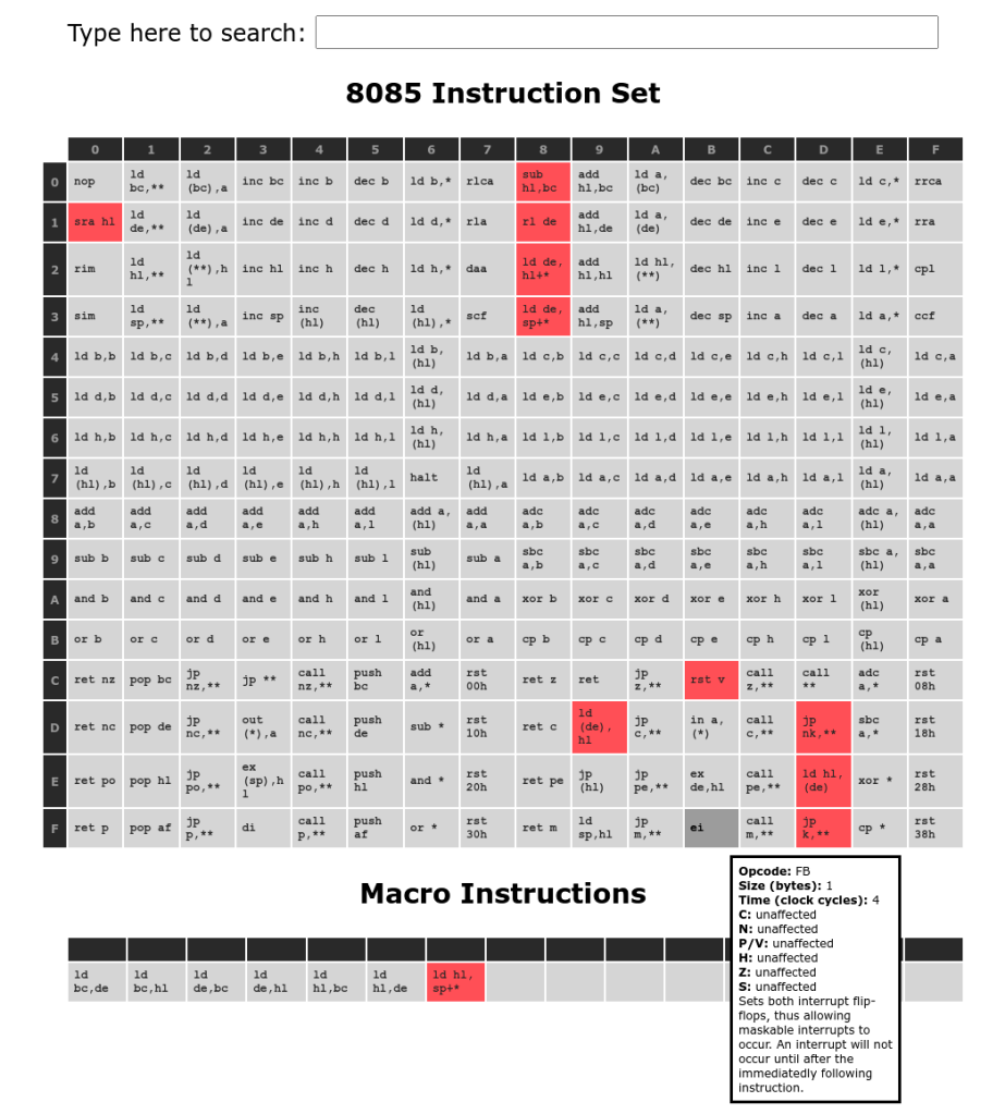
8085 Extended Instructions
Over the years since launch 10 very useful extended instructions designed into the 8085 have been found and documented. These instructions are particularly useful for building stack relative code, such as required for high level languages or reentrant functions. However, perhaps because of corporate politics, these useful instructions were never announced, and thus were never widely implemented. These instructions remained effectively undocumented until they were formalised in the Tundra CA80C85B CPU datasheet.
The z88dk-z80asm assembler also provides synthetic instructions to simplify code for the different variants (it has also recently become a macro assembler) to simplify programming. These instructions are usually a useful sequence of normal instructions that can be issued with no side effects (eg. setting flags) that may streamline combined 8085 / z80 programming.
8085 Instructions implemented by z88dk z80asm assembler
Discussion on the Extended Instructions
Some things to think about (and then do).
Use the Underflow Indicator (K or UI) flag with 16 bit decrement and JP K, JP NK instructions to manage loops, like LDIR emulation, more cleanly. 16 bit decrement overflow flag K is set on -1, not on 0, so pre-decrement loop counter.
Use the LD DE,SP+n instruction with LD HL,(DE) to grab from and LD (DE),HL to store parameters on the stack. Can use this with a math library to make it reentrant, for example, and also relieves pressure on the small number of registers.
Use the LD DE,SP+n instruction with LD SP,HL to quickly set up the stack frame. For example LD HL,SP+n, DEC H, LD SP,HL to establish 256-n stack frame.
Use RL DE together with EX DE,HL to rotate 32 bit fields.
Use RL DE together with ADD HL,HL to shift 32 bit fields.
Use RL DE as ADD DE,DE to offset into tables and structures.
Use SUB HL,BC for 16 bit subtraction, and for comparative operations.
Remember EX (SP),HL provides another “16-bit register”, if SP+2 is made the location of the return by pushing to create a register, and SP+4 then becomes the location of first variable.
Use the K flag together with JP K,nnnn to improve signed integer comparison operations.
Since we know that the 8085 extended opcodes are available in every 8085 device they can be relied upon for any 8085 system. The challenge will be to take existing 8080 programs, such as Microsoft Basic and CP/M, and implement improvements using these 8085 specific instructions.
In reworking the z88dk sccz80 l_ primitives to make them reentrant and to optimise them for the 8085 CPU, I have found the LD DE,SP+n instruction very important. Using this instruction it is possible to use the stack effectively as static variable storage locations. The alternative available on the 8080 (and Z80) LD HL,N , ADD HL,SP takes 21 cycles, and clears the Carry flag. With the few registers available on the 8080 losing the Carry flag to provide state causes further cycle expense, spared with the 8085 alternative.
To load a single stack byte using LD DE,SP+n , LD A,(DE) is only 4 cycles slower than loading a static byte using LD A,(**). Also, loading a stack word using LD DE,SP+n , LD HL,(DE) is only 4 cycles slower than loading a static word using LD HL,(**). Given that variables can be used in-situ from the stack or pushed onto the stack from registers rather than requiring the overhead of the value being previously loaded into the static location, this small overhead translates into about 3 stack accesses for free compared to static variables.
One small design oversight in the Program Status Word of the 8085 is however quite annoying. The flags register contains a single bit that always reads as 0. A $FFFF pushed to AF is read back as $FF7F. This means that unlike in the Z80, it is not possible to use a POP AF , PUSH AF pair as a temporary stack store, which invalidates AF as one of the only 3 additional 16-bit registers as an option, making things even tighter when juggling the stack. I’d call it annoying AF.
The RL DE and SUB HL,BC instructions are very useful to build 16-bit multiply and divide routines effectively. They have contributed to useful optimisations of these primitives. The saving in bytes over equivalent 8080 implementations has allowed for partial loop unrolling, which also speeds up the routines by reducing loop overhead. Initially, I was concerned that the SUB HL,BC function didn’t include the Carry flag. But in hindsight it is not possible to effectively carry into the registers, and using the 8 bit SUB A,C , SBC A,B instructions via the A register is the way to manage long arithmetic.
Recently the LD DE,SP+n and LD HL,(DE) or LD A,(DE) instructions were used to replace the sccz80 z80 stack access routine LD HL,n, and ADD HL,SP followed by CALL l_gint or CALL l_gchar. Also the stack store routine CALL l_pint was replaced by LD (DE),HL. These small changes to the optimisation process have substantially improved the 8085 benchmarks, in both code size and performance, and now they are often on a par with similar z80 benchmarks.
More recently I’ve been wondering about the sub hl,bc instruction. Why was it so important to have a subtraction instruction when two complement numbers can be subtracted easily using the addition instruction? Why did sub hl,bc win its place in the limited opcode space?
Well it turns out (I believe anyway) that the 16 bit subtraction instruction sub hl,bc is really intended for efficient comparison operations. In C it is quite common to end loops with equality ( == ) or inequality ( != ) operators, and these can be quickly implemented with the sub hl,bc instruction. Subtracting two numbers quickly generates a signal (zero flag) to either equality or inequality depending on what you want to test.
So I recently included special cases of equality and inequality comparisons using sub hl,bc into the z88dk 8085 library support. The improved 8085 equality operation looks like this, compared to the original 8080 compatible version here. And as a result the regex library function test is now faster on 8085 than it is on z80!
Also all signed integer comparisons can be optimised through use of the K flag and sub hl,bc which brings them to the same performance as the z80.
CP/M-IDE 8085
The next challenge was to build a CP/M-IDE version for the 8085 CPU. The ingredients are ACIA serial drivers adapted for 8085, IDE (or Compact Flash) diskio drivers for 8085, and the ChaN FatFs library compiled for 8085, plus a 8085 adapted BIOS.
Modules required for CP/M-IDE 8085
When looking at the IDE drivers written previously for Z80 it was obvious that I’d gone out of my way to use Z80 instructions, which were actually slower than using 8080 instructions. So, I took the opportunity to rewrite an integrated solution for both Z80 and 8080/8085, for future maintenance.
The new CP/M-IDE 8085 code is very similar to the existing ACIA and SIO serial Z80 code, by design. I’ve tried to minimise the differences where ever possible. The remaining differences are mainly in the BIOS code, and relate to initialisation of the 8085 interrupts and the different CRT code used between Z80 and 8085 systems.
To use the APU math library with CP/M, the library just needs to be linked with --math-am9511. For example: zcc +cpm -clib=8085 -v -O2 n-body.c -o nbody --math-am9511 -lndos -create-app
The Whetstone Benchmark for RC2014 results (7.3728MHz, hand timed) are:
8085+MBF32 -> 78.2 Seconds -> 12.8 kWhetstone.
8085+AM9511 -> 30.4 Seconds. -> 32.9 kWhetstone.
And for the n-body Benchmark the RC2014 results (7.3728MHz, hand timed) are:
8085+MBF32 -> 252.3 Seconds.
8085+AM9511 -> 69.3 Seconds.
So the 8085+APU system is 2.5x to 3.6x faster than the best 8085 software maths library. And what is also interesting is that these numbers align very closely with the Z80+APU results.
The 8080 CPU stands at the root of microprocessor development over the past 50 years. Although it was the first commercially successful device, it was followed quickly by two different processors with different bus characteristics. This is a record of interfacing one of the descendants, the Intel 8085, with peripherals and modules designed for use with the other descendant, the Zilog Z80.
All three of these devices, the 8080, the 8085, and the Z80 were implemented with 40-pin DIP packaging, which limited the number of pins they could use for bus signalling. The 8080, requiring 3 power supply voltages, was particularly limited as it didn’t multiplex the address or data lines, but rather needed to share the data lines for status information. More about the 8080 can be read at Wikipedia, or CPU Shack. I will not add to it here.
Derived from the 8080 and implemented by the same lead designers and architects, the Zilog Z80 uses four lines to signal general timing on the bus. In addition, a M1 line is used to signal that an interrupt is being processed and that an interrupting peripheral needs to provide an address (or vector) to which the CPU should jump in IM2 mode.
The Z80 rationalised the power requirements down to +5V and GND, which allowed a simpler and more explicit set of bus controls to be provided. As the Z80 implemented two address spaces, one for memory and one for Input/Output ports, it was useful to have two separate lines signalling memory access and Input/Output access. In this way a peripheral only needed to handle one of the two signals, depending on whether it was memory or a I/O address space peripheral device.
In addition the Z80 has two lines providing signalling for Read or Write. The timing was designed so that the data on the 8 data lines was valid at the point when the respective signal was deasserted. The Z80 would hold data it wanted to write or output until the write signal was deasserted, and it would latch and read the bus when reading or inputting data when the read signal was deasserted.
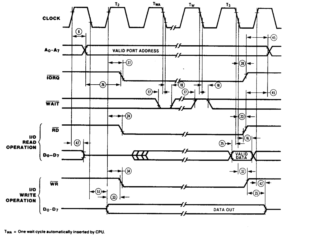
Z80 I/O Cycle Timing
With only minor differences, the Memory and Input/Output lines are operated with similar timing, and this is aligned mostly with the Read and Write signals. This enabled system designers to build very simple bus interfacing for their Z80 based systems.
There are many additional features and alternatives here, around Interrupt Mode 2, timing for sampling the Ready pin which causes the Z80 to pause, and other minor timing issues. However, they are not relevant for most purposes.
Most system designers used these four signals to create memory write, memory read, I/O write and I/O read signals. Then one signal line, together with a chip-select generated by the address lines (directly in simple systems, or through logic in more complex systems) was enough to operate each component of the system.
For the 8085, the Intel architects took the bus interface in another direction. They integrated several components from the support chips for the 8080 into the silicon die, and produced new features which made the 8085 much more useful as a micro-controller than the Z80. For the bus, the major change was to multiplex the data lines with the low address lines. This step allowed them to reuse the 8 saved lines on the 40-pin DIP for other purposes.
Multiplexing the address and data lines meant that they had to add an external address latch, to capture the lower address values, before either writing data or reading data from the bus. The normal read and write lines are present and they behave in a similar manner to the Z80.
In a significantly different solution to the Z80, the 8085 uses only one line to differentiate Input/Output and Memory addresses. Using the sense of the line high or low to indicate whether the I/O address space or the memory address space is being addressed. The timing on this IO/M line is also substantially different to the Z80, where here it is valid for the entire cycle of an instruction. It does not become valid when the bus address is valid, rather it is valid from the start of the instruction through to the completion of the instruction.
8085 General Cycle Timing
This is the first significant divergence from the Z80 system bus, and it causes issues with peripherals that require an enabling signal to be provided after the address lines are stable. In most designs a decoder was required to produce signals for attached peripherals.
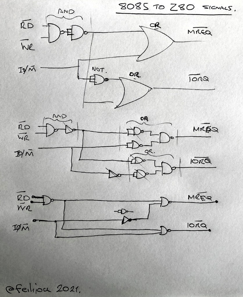
Generating Z80 /IORQ and /MREQ from 8085 signals
As many Z80 standard peripherals and also Motorola peripherals need to have the /IORQ line valid when the address is stable, we need to generate a Z80 compatible /IORQ (and /MREQ) signal. There are textbook “decoder” circuits available to produce the four system signals /IOR /IOW, /MEMR and /MEMW from the 8085 IO/M signal and /RD, /WR, but there is no standard solution for using the 8085 on the Z80 bus. This problem we are going to solve.
From the Z80 datasheet the /IRQ and /MREQ signals are almost exactly tied to the timing of the /RD and /WR signals. Therefore we can use /RD and /WR with some combinational logic to produce mostly correct timing for /IORQ and /MREQ. We need to have a valid signal when either /RD or /WR is low (active). If both are high, then the result should be also high (inactive). Both /RD and /WR are never active, but for convenience we can let the result be active if both are. In positive logic this would be generated by an OR gate. But with inverted logic (active low) this is implemented as an AND gate.
/RD
/WR
Result – /RD./WR
0
0
0 – Invalid state.
0
1
0
1
0
0
1
1
1
Intermediate Truth Table
To generate the /MREQ signal we are looking for the time when IO/M is low whilst either /RD or /WR is low. In negative logic this is an OR gate, where the signal remains high unless both /MREQ and /RD or /WR are low. So to generate /MREQ we need to provide ( /RD AND /WR ) OR IO/M.
/RD./WR
IO/M
Z80 /MREQ
0
0
0 – Only when both are active.
0
1
1
1
0
1
1
1
1
To generate the /IORQ signal we can recognise that it is simply the same /RD /WR logic but the IO/M line needs to be inverted or NOT converted. So we can generate /IORQ by ( /RD AND /WR ) OR NOT IO/M.
From this solution we can simplify the expression into either NAND or NOR gates. Taking NAND gates as the basis the solution can be simplified into 4 gates that can fit into a 7400 device.
Converting 8085 signals to Z80
Other Bus Timing Issues
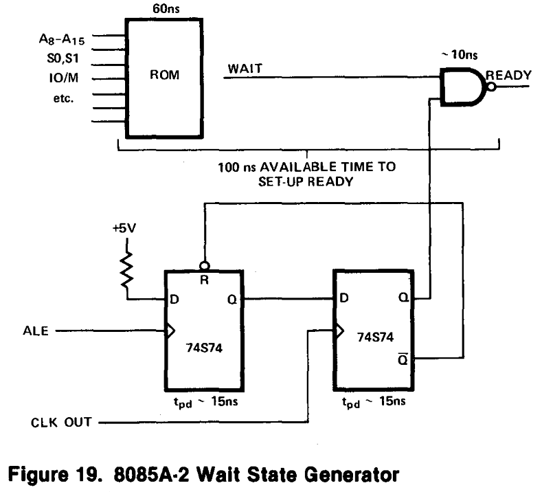
Several Z80 peripherals use the READY signal to cause the Z80 to wait until they are ready to read data from the bus, or to write data onto the bus. The Z80 implements one wait state whenever it uses I/O instructions, to enable slow peripherals sufficient time to signal they are not READY to proceed. The 8085 does not add in the automatic wait state, so there may not be sufficient time for them to signal the CPU to wait. There are standard circuits available to add one wait state into 8085 bus cycles.
Motorola bus peripherals use an E or Enable clock to signal that they are being addressed. For the Z80 bus, this is typically implemented by inverting the /IORQ signal. However, for the 8085 using the method above, there may be insufficient time between the E (inverted /IORQ) and stabilisation of the address.
Z80 peripherals capable of Interrupt Mode 2 use the M1 signal to determine when they should place their interrupt address (vector) on the bus. The 8085 does not generate this signal, but since the 8085 does not support IM2 mode anyway this point is probably moot.
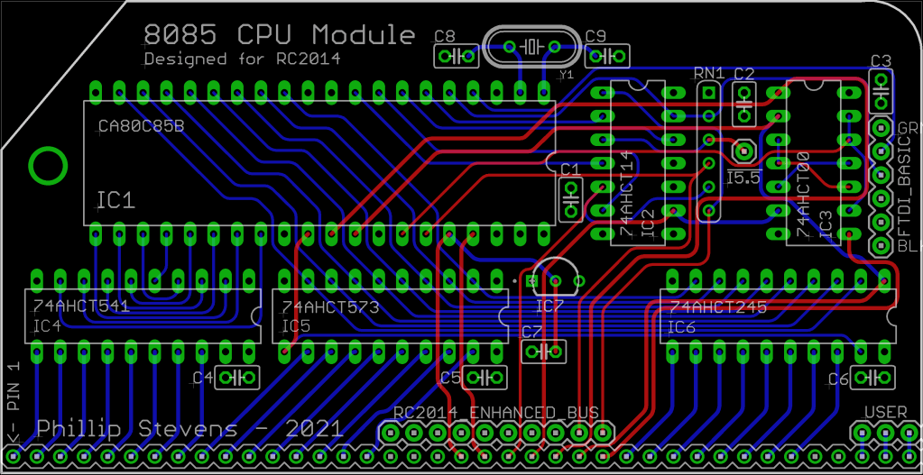
8085 CPU Module for RC2014
8085 CPU Module PCBs are available on Tindie. Combine with a Memory Module PCB to save postage.
The RC2014 Bus and Modules have been available now for some time, and the Z80 nature of the system bus provides for simplicity in the system design. There is no buffering or conversion by the CPU Module, and individual peripheral Modules are left to convert bus (or Z80) signals to suit their own requirements.
I have previously designed a few Modules for the RC2014 and, since I’ve now an interest in 8085 processors, I thought that it would be a good time to design a 8085 CPU Module.
In researching the requirements for a 8085 CPU Module to work with the RC2014 Z80 bus and standard peripheral Modules, I found the Glitchworks 8085 SBC and also Alan Cox’s 8085 designs. My initial design replicated the bus interface signalling of these two designs.
After building the first version of the 8085 CPU Module I found that the Motorola 68B50 ACIA based RC2014 Serial Module didn’t work properly. This is because on the module the required E clock is derived from Z80 /IORQ timing, and the simple method of inverting IO/M as /IORQ doesn’t provide the timing needed. The 68B50 requires the bus address to be stable before E (or /IORQ inverted) is asserted.
A second version of the 8085 CPU Module was implemented, using the above method for generating the /IORQ and /MREQ signals.
Further analysis on the performance of AHCT buffers vs unbuffered I/O to come.
Please read further for software support, including undocumented instruction discussions.
RetroChallenge 2021/10 – Am9511A APU Support
The current hardware doesn’t supply a wait state to the CPU, so the hardware interface to the APU Module designed for RC2014 doesn’t work. The 8085 CPU allows only 25ns to 30ns (depending on the manufacturer specification) for assert not READY (or /WAIT). Am9511A takes 83ns to assert /WAIT.
The retro-challenge is to extend the current 8085 CPU Module design to include a wait state generator for IO instructions to support the APU Module and the UX Module.
Retrochallenge – 1st Update – 2nd October
Getting to Am9511A APU support for the RC2014-8085 machine means firstly getting the fundamental 8085 platform working.
The RC2014 is supported by the “newlib” of Z88DK, which is meant for Z80, Z180, Z80N (Spectrum Next) processors, and the 8085 is supported by the “classic” library. So this is the first time that a newlib machine is using classic lib libraries. Confusing? Yes I find it so.
Anyway the trick is just getting the right pieces to link together. Having ZIF ROM and TL866CS Programmer helps with fast programming cycles.
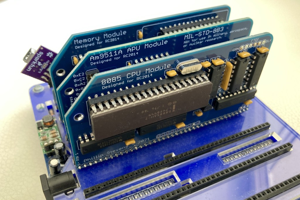
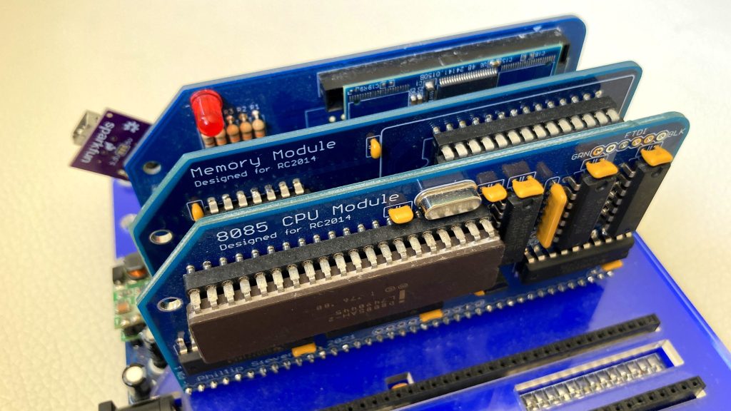
RC2014 – 8085 CPU Module, APU Module, and Memory Module
Retrochallenge – 2nd Update – 3rd October
Now the z88dk RC2014-8085 ROM build using the ACIA Serial Module is working (along with the RAM build supported by Basic), I’ve spent the past days tidying the ACIA builds around my various repositories, to keep everything consistent. So now my BASIC builds for both 8085 and Z80 are aligned with RC2014 HexLoadr BASIC, CP/M-IDE ACIA, and also the z88dk ACIA newlib device code. Also took the time to clean up some the SIO device code too.
@suborb is working on the z88dk classic library crt0 and compiler intrinsics, as they’ve been stuck in both classic and newlib and are a bit disorganised. Hopefully the result will be one set that can be used for both compilers (zsdcc, and sccz80) and both libraries, across multiple machines (8080, 8085, GBZ80, Z80, Z180, Z80N, etc) which will make maintenance much easier.
Waiting now for China to come back from National Day holiday, so I can get started with new hardware.
8085 Wait State Generator
Retrochallenge – 3rd Update – 8th October
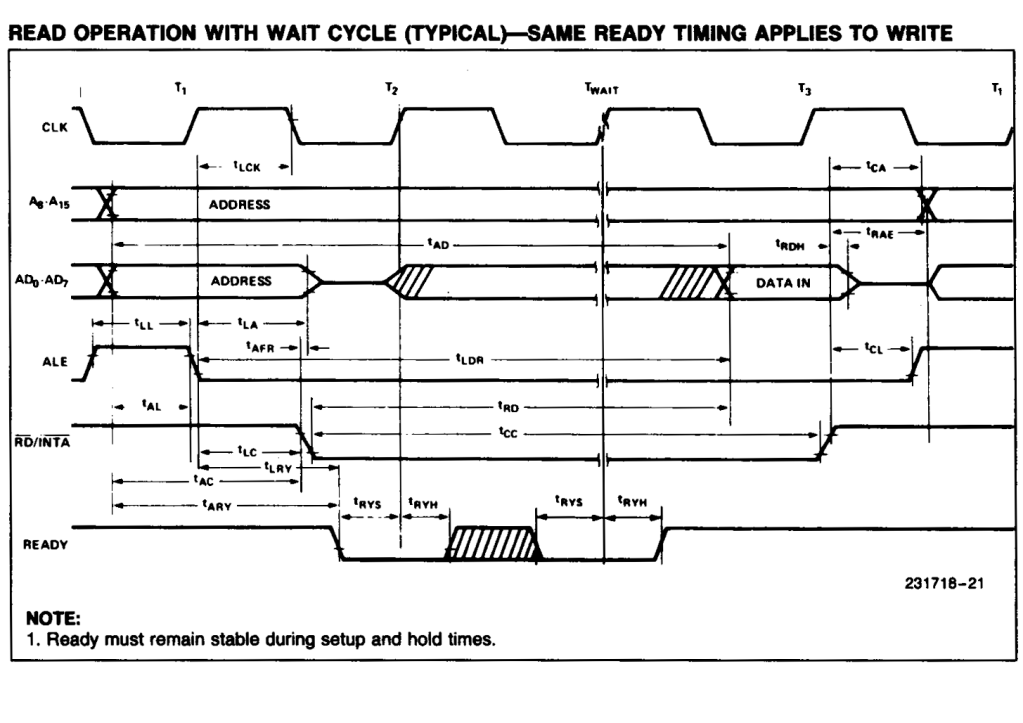
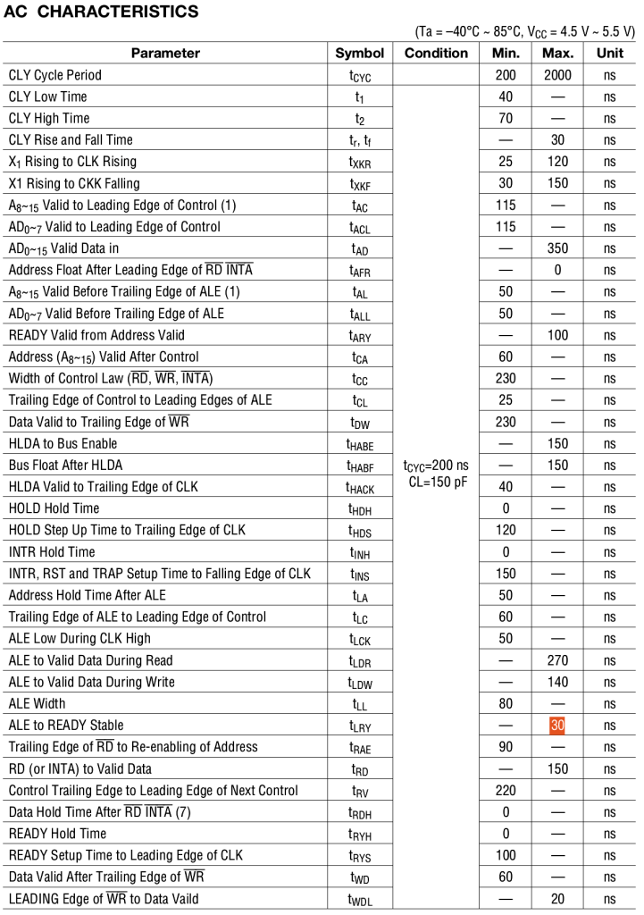
As noted above the window of opportunity for a 8085 bus peripheral to signal not READY is very short. In fact is is no more than 30ns from fall of the ALE signal, and this is 30ns before the /IORQ signal is even enabled.
8085 Timing showing ALE fall to /READY as tLRY.
Timing information from the 8085 datasheet shows tLRY as maximum 30ns, and tLC as minimum of 60ns.
8085 CPU Timing – compare tLC to tLRY
To be able to connect devices designed for the Z80 bus to the 8085 CPU we will need to implement a wait state generator. In the best case this will only affect I/O cycles, and will not slow down normal memory read and write cycles.
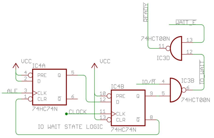
Designing the 8085 /IORQ Wait State Generator
As the need to generate a wait state was well known at the time of release of the 8085, several sources include the information required for the design of a basic solution. It is left to the reader to determine how to use the created wait state though.
For our purposes we need to have a wait state generated only for peripheral devices, accessed using the I/O instructions. Therefore we can modify the above circuit to only generate a wait state when the I/O address space is active, or when the external Z80 bus /WAIT signal is active. The below circuit produces a /READY signal that provide 1 wait state whenever the I/O address space is active, and can continue to produce wait states until the /WAIT signal is de-asserted.
As the static RAM / EEPROM memory devices we are using are not sensitive to the timing of the /MREQ signal, the NAND gates assigned to generate a correct Z80 /MREQ have been recovered and reused in the implementation of the wait state generator. Therefore the revisions required only one additional device on the PCB. Based on this design a revised 8085 CPU Module was created, and ordered. Due to arrive around October 18th, which won’t leave much time to finish before the end of the RetroChallenge. It will be a rush, as usual.
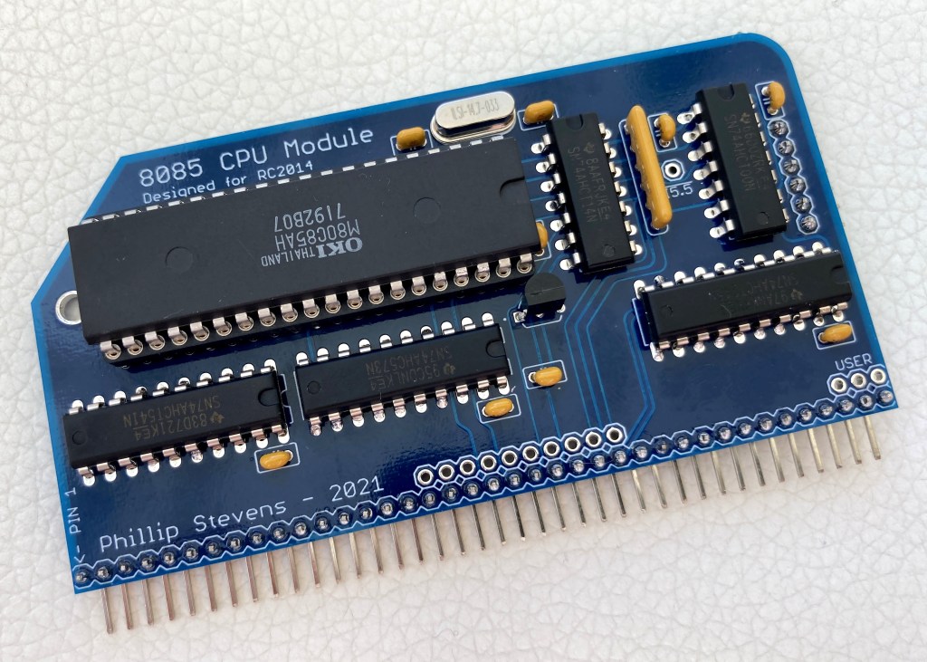
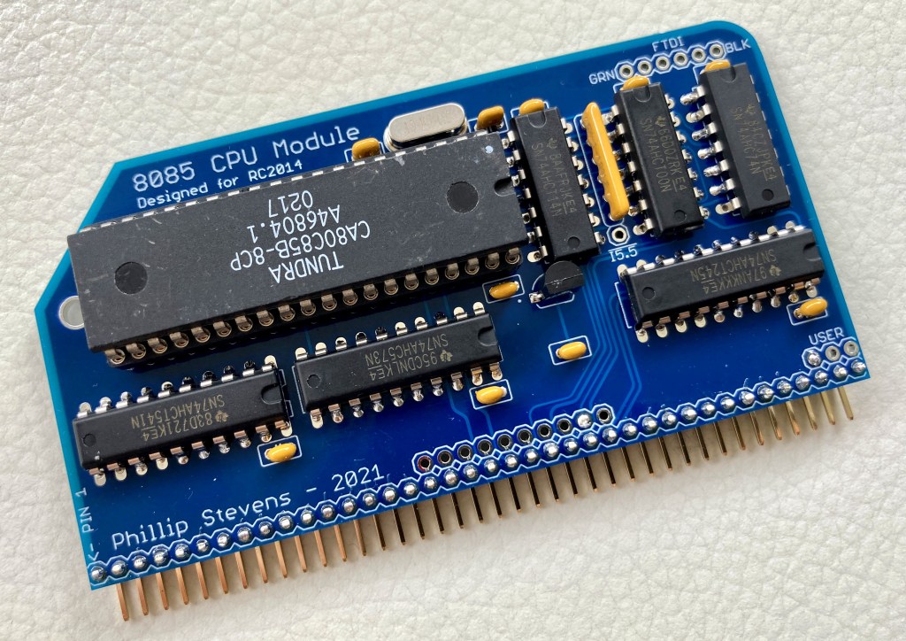
The new 8085 CPU Module PCB arrived, so wasting no time I’ve build one up to test. And it works!
8085 CPU Module – Version 4
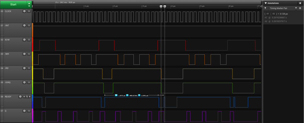
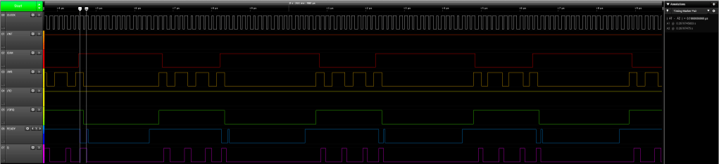
It is interesting to look at the signals actually appearing on the RC2014 Bus during the operation of the APU. Here we have a floating point read from the APU, 4 bytes, where the wait state generator produces sufficient delay (1 wait state) to allow the APU to generate its own /WAIT signal for the last two bytes.
8085 CPU Module – APU Read Cycle
The floating point write cycle is similar but the duration of the /WAIT signal from the APU is longer, and the APU needs to assert it on every byte written. Note that tRYH is 0ns, so there is no need to hold the /READY signal beyond the clock rise point.
8085 CPU Module – APU Write Cycle
To support the Am9511A APU Module the /WAIT signal has to be patched to the USER1 Pin (if using the standard RC2014 backplane), which allows the Am9511A to extend the single wait state generated by the 8085 CPU Module for as long as the APU needs.
8085 CPU Module shown together with Am9511A APU Module and Memory Module (160kB).
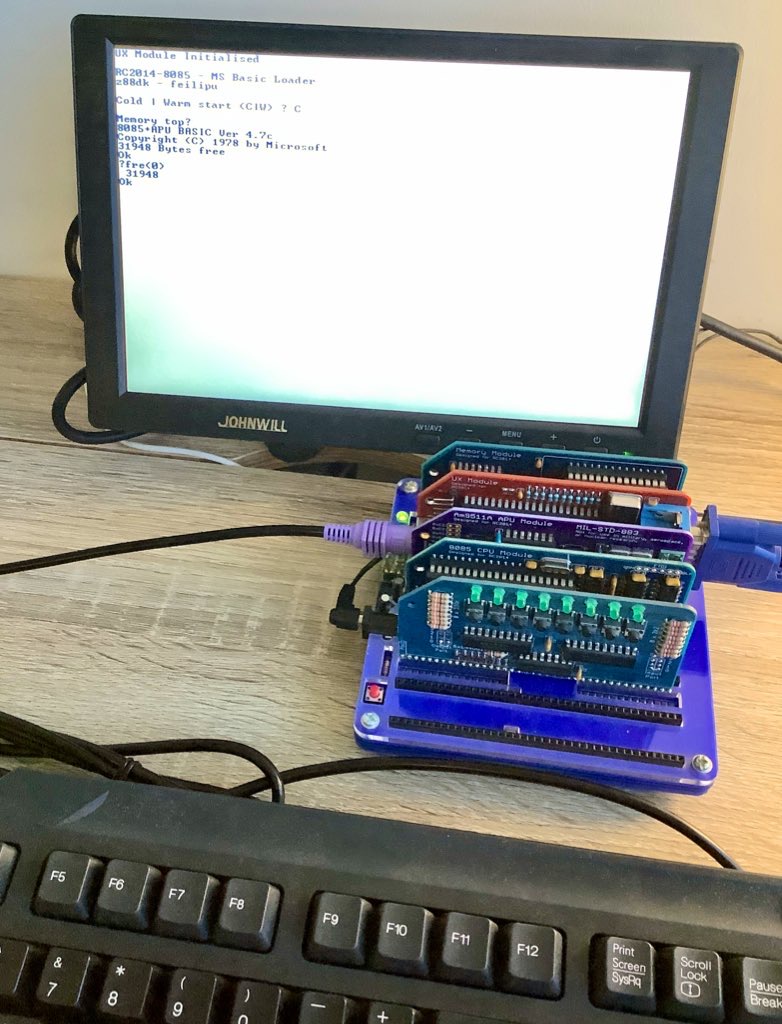
With the Wait State generator functioning, it is now possible to use the UX Module for a VGA screen and PS/2 Keyboard.
Stand-alone 8085+Am9511 RC2014 System.
Retrochallenge – 6th (Final) Update – 26th October
Rework of z88dk classic 8080/8085/gbz80 library l_ functions.
When working with the 8085, the biggest issue is the continual pressure on the few CPU registers. Alongside the 8-bit accumulator a register and the 16-bit accumulator hl registers we have only two additional register pairs that can be used, the bc and de registers. This gives the system programmer few options but to use static memory locations to store intermediate values, which leads to non-reentrant code.
Having non-reentrant code is normally not a problem, but it does lead to issues when multiple threads (or tasks) are trying to use the CPU at the same time, for example when a multi-tasking operating system is to be supported. So it is useful to try to build reentrant functions that use the stack for storage of intermediate values, rather than static memory locations.
The designers of the 8085 had this in mind when they designed the additional functions found the 8085 silicon. The “new” instructions make it very efficient to build stack relative functions (compared to the 8080), and this relieves some pressure on the small number of registers.
However, there was one oversight made by the designers, as the 8085 af register pair cannot be used, in contrast to the z80, to pop and push arbitrary words on the stack. This reduces the number of available 16-bit registers by 1 of possible 4. There is one flag bit that always reads as 0, which is an subtle but annoying limitation of the 8085.
As background, some of these functions originate from the 1980s and 1990s in the Amsterdam Compiler Kit, and haven’t been updated or improved for the past 20 years. They weren’t broken. But they were in need of some attention.
So this update is the final one in the October 2021 RetroChallenge. All the new functions are checked in and are now part of the z88dk.
8085 CPU Second Sources
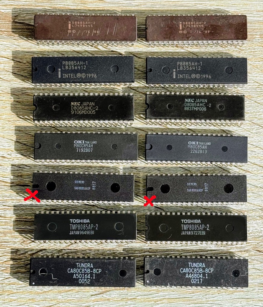
Recently I purchased some second source 8085 CPUs, and an additional Intel OEM option to test. As the RC2014 System runs at 7.3728MHz, beyond the specification of most of the 8085 CPUs below, it is very gratifying that all of the selected second source CPUs function correctly, with just one exception.
8085 CPUs Tested
Some very simple testing was done to determine how much current each CPU implementation required, and from this it is clear which devices are implemented in NMOS, and which in CMOS. Only the OKI and Tundra devices seem to be CMOS.
To get an approximate base line current requirement the CPU was unplugged and the remaining power requirements were measured. Two different measuring methods were used, which don’t quite align, but the relative results are quite consistent.
Selected 8085 CPUs with approximate operating current
Personally, I keep both Intel CPUs in my 8085 CPU Modules. The original ’76-’80 ceramic D8085AH-2 looks good paired with a similar vintage Intel 8231 APU. As a daily usage system, the 1996 release (20 years more recent) P8085AH-1 is specified to 6MHz and is (with the exception of the modern CMOS Tundra device) the closest specification to the RC2014 CPU Frequency. But realistically it makes no difference which one you use.
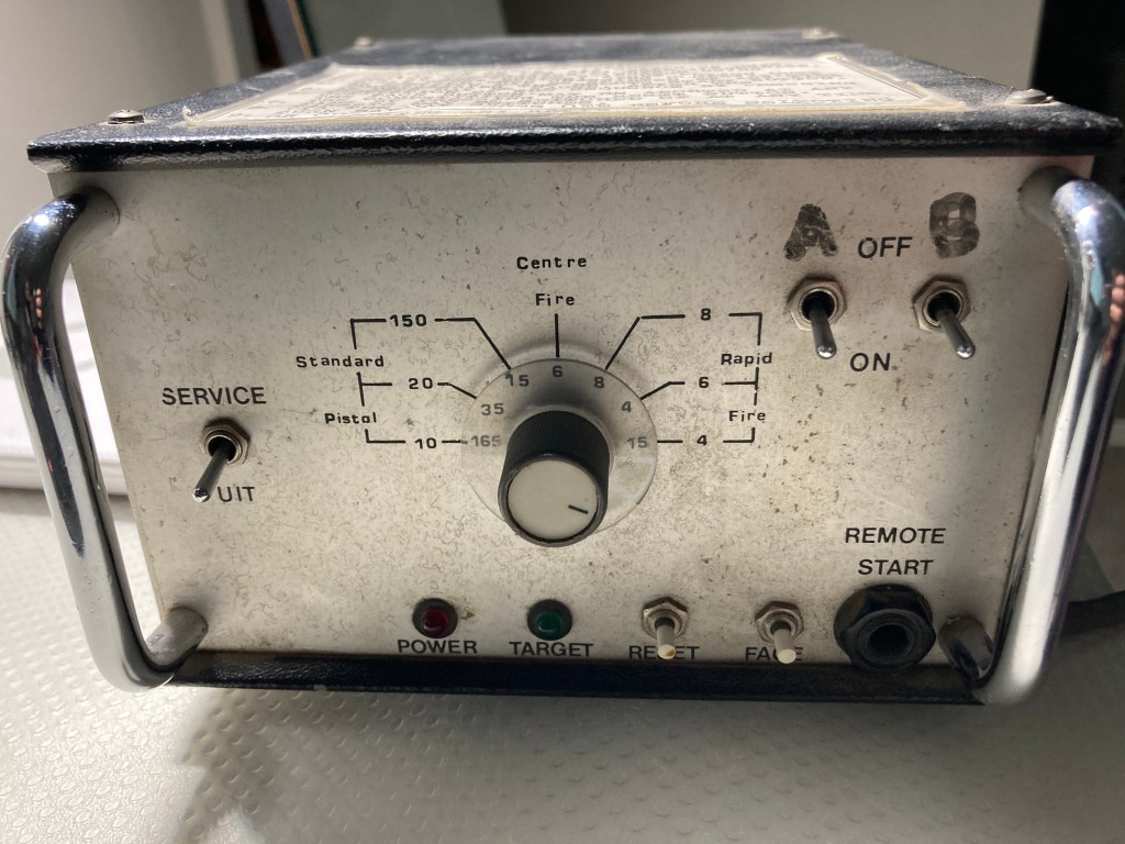
My club uses pneumatic systems to turn the ISSF Targets, which are controlled by a timing system. One of the members asked me to help build a phone interface for the systems.
The systems are used for many courses of fire, and there are quite a few options to manage. On the front panel there is a RESET, which is tied to the CPU RESET, and a FACE button which returns the targets to face the shooter for scoring.
Target Turner Front Panel.
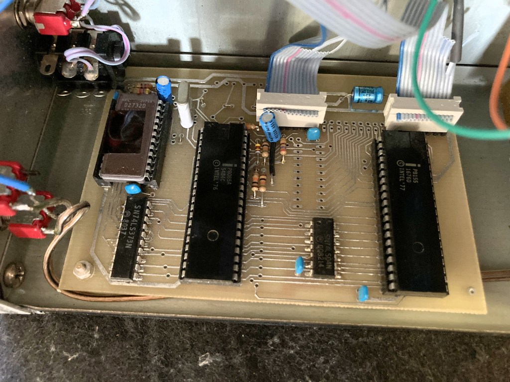
It turns out that the retired systems are based on a 8085 CPU, in the classic minimum configuration with an 8155 providing 256 Bytes of RAM, and input and output ports. There is a 2732 UV PROM holding the program.
CPU Board for the Target Turner.
So, how do we get these devices online? My thoughts are to add a serial port so that the system can be controlled remotely, then to use an additional WiFi enabled device which can present a web interface to the Range Officer to control proceedings.
Existing ROM
First step is to see what is going on under the hood here. So using the TL-866 the binary code on the ROM was read, and then using z88dk-dis the existing code could be interpreted.
It was interesting to see a very simple method of operation in the existing ROM. The system can only change course of fire if it is RESET, when it reads the position of the switches, and then halts awaiting an interrupt to trigger the course of fire. When the string is finished it will return to repeat the same course of fire.
Timing was based on a delay circuit providing 500ms of delay per unit. Perhaps it is not 100% accurate, but good enough for the application.
I believe that I found a bug that has been latent in the device for the last 40 years. It seems that an address byte was reversed, which would cause a jump into empty addresses. Not sure why no one realised that previously.
Building Serial Interface
I’m planning to build a simple serial interface which will read a character, and then change the course of fire based on that character. Initialising the course of fire can be then done by the web interface, by triggering an interrupt, or by using the wired front panel interface.
After asking the experts I learned that the SID/SOD pins on the 8085 can be used as a bit-bang serial port. In fact that is the standard way of building a serial port for early systems. The code for building serial transmission is included in the early application notes.
The serial code works perfectly at 9600 baud on this 3MHz system. Since only one character will be received and a few transmitted on boot, there are no performance issues to consider.
I’ve written the upgrade code to replicate the front panel selection process, and to allow the system to behave exactly as before when no serial input is available. When a serial command is available, which is triggered by activity on the RST6.5 line, then the system will set a different course of fire than is shown on the front panel. The string can be triggered either by the front panel, or by the interrupt related to the serial interface.
ESP-32 Web Interface
Following a bit of a search the Adafruit HUZZAH32 Breakout presented itself as the best solution to web enable the Target Turner. It can be powered by 5V, and the RX is protected against 5V input by a diode.
The physical interface is going to be a FTDI Basic style connector. Using this connector will allow me to best the 8085 first, and then build the web interface and test separately from the Target Turner. The last step will be to integrate the two devices into a system.
Using the simple serial character interface, it should be possible to present an active web page to the Range Officer.
There are many, eg, tutorials on how to build active web pages using the ESP-32 and WebSockets.