Characterising Am9511A-1 APU

I’ve built two hardware solutions supporting the AM9511A APU. Partly for historical enjoyment, and partly because the AM9511A is actually still faster at floating point and 32-bit long arithmetic than “modern” Z80 devices.

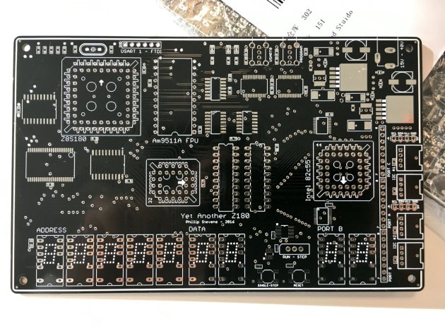
I’ve built a Z180 based board, the YAZ180, which runs the AM9511A at 2.304MHz. And I’ve built an APU Module for the RC2014 platform, which runs the AM9511A at 2.4576MHz. Both of these solutions are supported by the z88dk am9511 maths library and platform drivers for Z80, Z180, and 8085 CPUs.

To compare the performance, for example, from the Am9511/Am9512 Floating Point Processor Manual we have some comparison tables. On average the Am9511A APU (at 1.966MHz) produces a hardware floating point divide in 165.9 cycles (of a 2MHz 8080 processor). Converted to my YAZ180 Am9511A implementation (at 2.304MHz), we have the equivalent in 141.5 cycles of the 2MHz 8080. Converted to best case modern Z180 terms (overclocked to 36.864MHz) this is 2,609 CPU cycles to return a hardware floating point divide.

To produce an equivalent software floating point divide, using the equivalent vintage LLL floating point library, requires 13,080 cycles.

This means that floating point on the 40 year old AM9511A-1 APU is still 5.0 times faster than an overclocked Z180 running antique 8080 code. Sweet!

Testing

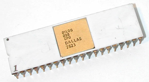
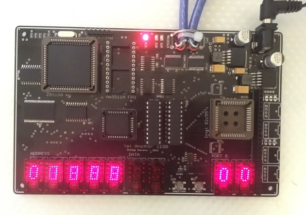
I’m integrating an Am9511A-1 APU device into my YAZ180 build. The basic device is capable of operating at 3MHz. But, I’ve found that driving one sample at 3.072MHz doesn’t work. But, it works fine at 1.536MHz, and at 2.304MHz.

This one example has 83.33ns delay between RD or WR and PAUSE signal being operated. This means that it should comfortably operate with the minimum of one wait state when the Z8S180 is running with a 18.432MHz bus.

And, I’ve got to say that these devices run hot… OHS issue hot. There is a reason they are provided in a ceramic package. They sink 70mA at 12V plus another 70mA at 5V, and all that energy has to go somewhere.

Originally, I had created the timing for the Am9511A-1 is generated by dividing the Z8S180 18.432MHz system clock by 6. The divide FCPU by 6 for FAPU CLK 3.072MHz is done with a SN74LS92N device. And for test purposes, the Z8S180 is also half rate clocked at 9.216 MHz, producing 1.576MHz for the APU.

img_0620

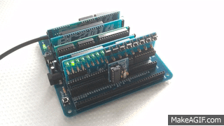
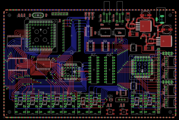
YAZ180 Test Rig – Am9511A-1

Initial Testing

The test is initially pretty simple, really just a proof of life. Will they properly push and pop data at 3.072MHz?

If not, then I’ll need to redesign the YAZ180 to operate the Am9511A-1 at a lower APU clock. But, if my initial samples are just not the up to specification, then they can be secondary devices.

Ok, now what kind of devices have I got to hand, and lets see what the results are…

Front Serial ID Country & Rear ID 3.072MHz 1.576MHz
239KH2Z Malaysia 9237FP Fail Pass
301MBZP Malaysia 9252CP Fail Pass
3368YF8 Malaysia 9335CP Fail Pass
348W76S Malaysia 9347DP Fail Pass
921BDIV Philippines 8917WM Fail Pass

Kind of boring really. Pretty clear that AMD oversold the capability of its Am9511A-1 to run at 3MHz. Or, I’m not feeding them with the correct timing.

I’ll need to redesign the YAZ180v2 to provide a divided by 8 clock at 2.304MHz, and cross my fingers that they work at that clock rate.

Update September 2017

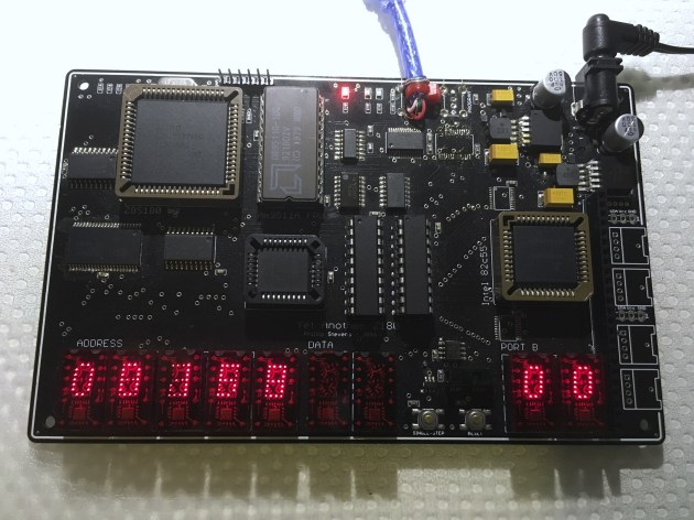
Following a substantial investment in testing of the solution in April and August, I’ve finally got a working system that can reliably use the Am9511A-1 to produce computational results.

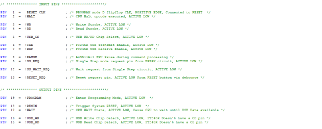
The main issue was described in the Retro Challenge period. The Z180 CPU I/O timing is slightly different to the Z80, in that it doesn’t provide any interval between the WR/RD deselection and the CS deselection. For most peripheral devices this isn’t a problem, but for some it causes them not to work. Hitachi recognised this problem, and provided a shortened I/O signal called the “E Clock”, which can be gated together with the WR/RD signals to gain the timing desired.

The Am9511A doesn’t require the RD signal to rise before the CS signal. Its TRCS time is 0ns. However it does require the WR signal to rise 60ns (or for Am9511A-1 30ns) before the CS signal. This can be achieved by gating the WR signal together with the E Clock signal. The Z180 E Clock is 1/2 a Phi cycle shorter than the WR signal during I/O instructions.  Therefore provided that the Z180 Phi is slow enough, then the required timing can be held. At 18,432MHz, the Z180 Phi signal is 54ns long, and therefore 1/2 Phi is 27ns, which is too short to work consistently. However, the Z180 can halve its Phi speed easily, and simply by changing the CMR register the Phi clock can be reduced to 9.216MHz, which in turn gives us (theoretically) 54ns TWCS for the Am9511A-1.

In practice gating the WR signal through the E Clock provides 41ns for TWCS, which is enough to work reliably with Am9511A-1 devices.

However, as the Am9511A-1 timing is derived from the Z180 clock (divided by 8), running Phi at 9.216MHz means that the APU is in turn under clocked to 1.152MHz. We can avoid this waste of capability, by managing the Z180 clock precisely during the command interrupt generated by the Am9511A-1. On entry to the interrrupt, we reduce the Phi to allow commands (TWCS) to work, and on exit from the interrupt we return the Phi to its original setting of 18.432MHz (and the APU to 2.304MHz). This also conveniently avoids having to modify the Z180 ASCI code to manage serial communications in the light of the reduced system clock.

I have also tested the Am9511A-1 using this revised WR to CS timing, with my original clocking of divide by 6 from Z180 system clock, or 3.072MHz, and it doesn’t work. This means that we actually do need to stay within the specification, and not overclock the APU.

z88dk Driver

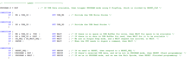
The z88dk supports the YAZ180 platform, so I have added a driver for the Am9511A into the device folders. The driver is based on an interrupt driven model. As noted in the Am9511A Processor Manual, there are 4 different models that can be adopted.

The Am9511A Pause signal is connected to the Z180 Wait signal, so if the CPU generates a request that requires time to fulfil, then the APU will cause the CPU to Wait by signalling Pause. Clearly this means that the CPU cannot do anything while it is in Wait mode. This model of working is called Demand Wait, and it provides the fastest APU response, but doesn’t support using the CPU effectively.

The APU status register can be read without the APU causing a Pause response. Therefore the CPU can poll the APU by reading the status register. In this situation the CPU can continue profitably, but response to APU requirements (for new operands, or commands) is limited to the polling rate. As different APU commands can be completed in different times, the optimal polling time can be difficult to calculate.

The APU End signal can be connected to a CPU interrupt, and in the case of the YAZ180 it is connected to the NMI, which is then triggered at the end of each command, when the APU is ready to receive a new command. If the APU commands are buffered in advance, then using this interrupt mechanism the APU can complete a long sentence of commands “autonomously” and in parallel to the CPU activities, interrupting only when it needs to load a new command. This is the mechanism used in the z88dk driver.

Some ideas for creating an optimal interrupt driven driver for the Am9511A were inspired by reading “An Efficient Software Driver for Am9511 Arithmetic Processor Implementation”, B. Furht and P. Lee, 1984.

The final driver option is to connect the APU Service Request signals to the CPU DMA interface. In the YAZ180 these hardware signals are connected, and if desired a DMA enabled driver could be written to take advantage of this interface. However as only 4 bytes of information can be transferred in each load or unload command, at face value there seems to be little advantage in building a DMA software interface.

The C interface for the Am9511A driver supports direct access to the Am9511A, like the asm driver, and hopefully it can be integrated into the z88dk math library options, to support transparent usage of the APU where it exists.

Currently, some simple C interface code is now available on z88dk, which allows us to do performance testing.

Performance Testing

A simple test of seeking prime numbers exercises the floating point divide and 32 bit fixed point divide. This “brute force” method is not optimised for the APU as 4x 32 bit numbers must be loaded into the APU, but only two divides and a subtraction are done, for each calculation cycle. During the operand loading process, the CPU must also be slowed down to half rate, but since this is during an non-maskable interrupt there is little effect on the overall system.

So, some comparisons. First using Nascom Basic, we have a baseline, for seeking 1000 prime numbers.

20 PRINT "LIMIT";
30 INPUT L
40 FOR N = 3 TO L
50    FOR D = 2 TO (N-1)
60      IF N/D=INT(N/D) THEN GOTO 100
70    NEXT D
80    PRINT N;
90    GOTO 110
100   PRINT ".";
110 NEXT N
120 END

200 REM 124.7 Seconds (hand timed) - Z180 36.864MHz - Nascom Basic

Adding the Am9511A to the calculation, by doing the inner loop in assembly and calling the APU for the divide and subtract duties, does speed things up.

20  PRINT "LIMIT";
30  INPUT L
40  FOR N = 3 TO L
50    IF USR(N) = 0 THEN GOTO 100
80    PRINT N;
90    GOTO 110
100   PRINT ".";
110 NEXT N
120 END

200 REM 90.4 Seconds (hand timed) - Z180 36.864MHz - Nascom Basic

This is interesting, as the Am9511A is running at 2.304MHz (straight out of 1977), yet it is STILL faster than software on a 36.864MHz Z180.

Now, what happens when using the z88dk, to do the calculation in C?

void main(void)
{
  static signed long l, n, d;
  printf("Limit: ");
  scanf("%ld", &l);
  for (n = 3; n != l; ++n)
  {
    for (d = 2; d != (n-1); ++d)
      if ((float)n/(float)d == n/d) break;
    if (d == (n-1))
    printf("%ld", n);
      else
    printf(".");
  }
}

// 67.8 Seconds (hand timed) - Z180 36.864MHz - z88dk sdcc_iy
// 62.7 Seconds (hand timed) - Z180 36.864MHz - z88dk newlib

// zcc +yaz180 -subtype=basic_dcio -vn -SO3 -lm -clib=sdcc_iy --max-allocs-per-node200000 primesC.c -o primesC -create-app
// zcc +yaz180 -subtype=basic_dcio -vn -SO3 -lm -clib=new primesC.c -o primesC -create-app

Using the assembly math routines in z88dk is now the fastest solution. But, we’d expect C to be faster than Basic. What happens if we do the divides and subtractions in the Am9511A. That’s why we’re here.

void main(void)
{
  static signed long l, n, d, r;

  apu_reset( (void *) 0x2021 ); //INITIALISE THE APU with the NMI VECTOR ADDRESS

  printf("Limit: ");
  scanf("%ld", &l);

  for (n = 3; n != l; ++n)
  {
    for (d = 2; d != (n-1); ++d)
    {
      apu_cmd_ld( &n,   APU_OP_ENT32);
      apu_cmd_ld( NULL,     APU_OP_FLTD);
      apu_cmd_ld( &d,   APU_OP_ENT32);
      apu_cmd_ld( NULL,     APU_OP_FLTD);
      apu_cmd_ld( NULL,     APU_OP_FDIV);
      apu_cmd_ld( &n,   APU_OP_ENT32);
      apu_cmd_ld( &d,   APU_OP_ENT32);
      apu_cmd_ld( NULL,     APU_OP_DDIV);
      apu_cmd_ld( NULL,     APU_OP_FLTD);
      apu_cmd_ld( NULL,     APU_OP_FSUB);
      apu_cmd_ld( &r,   APU_OP_REM32);

      apu_isr();        // calls the ISR to trigger the process
      apu_chk_idle();   // blocks until the APU is idle

      if (r == 0) break;
    }
    if (d == (n-1))
      printf("%ld", n);
    else
      printf(".");
  }
}

// 94.9 Seconds (hand timed) - Z180 36.864MHz - z88dk

// zcc +yaz180 -subtype=basic_dcio -vn -m -SO3 -clib=sdcc_iy --max-allocs-per-node200000 @primesC_APU.lst -o primesC_APU
// appmake +glue -b primesC_APU --ihex --clean

Well the end result is (surprisingly) similar to using the Am9511A together with Basic. The issue is that it takes a long time to load and unload the operands to the APU, and to process (cast) them, and then we only do a relatively simple operation when they’re there. Relatively speaking for this test, we’re bound by the I/O rate of the APU, which is quite slow, and this does not demonstrate actual the compute rate of the APU.

APU_OP_ENT32
APU_OP_FLTD -  56-342 Cycles
APU_OP_ENT32
APU_OP_FLTD -  56-342 Cycles
APU_OP_FDIV - 154-184 Cycles
APU_OP_ENT32
APU_OP_ENT32
APU_OP_DDIV - 196-210 Cycles
APU_OP_FLTD -  56-342 Cycles
APU_OP_FSUB -  70-370 Cycles
APU_OP_REM32

However, this is still a good result. We’re comparing a modern overclocked z180 at 36.864MHz, with an ancient device, released in 1977, running at 2.304MHz. And, we have achieved comparable results.

Update July 2018

Over the past year I’ve done quite a lot with the Am9511A. One interesting application was using it to calculate a Mandelbrot set, and generate a text image.

From the point of view of drivers, I re-wrote the interrupt based driver to use a 3 byte operand address in the ring buffer, to support access to the full memory space of the Z180.

I also uncovered a hardware bug, which was caused because I was resetting the APU clock divider with the system reset. This meant that the APU was not getting 5 clock cycles with Reset held high, and would therefor not reset reliably. Removing the reset signal from the divider chip solved this issue.

Update January 2022

Over the past few years the Am9511A has proven itself to be a worthwhile companion in all of my Z80 and 8085 CPU systems. To date I’ve never had a functioning device fail, despite their very high operating temperature, and their performance advantage over Z80 software floating point libraries is proven.

Intel 8231A APU + Intel 8085 CPU

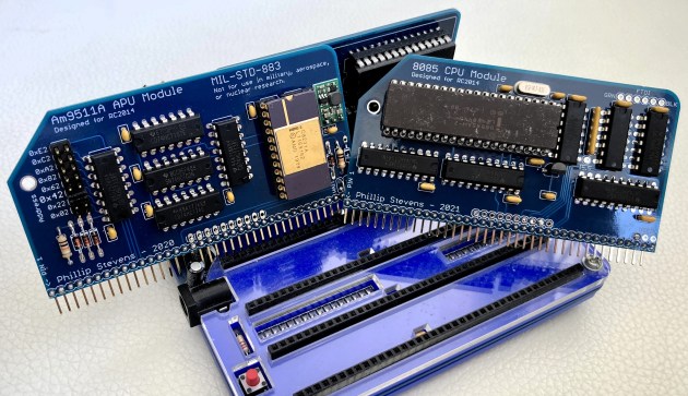
Intel 8231A APU Module with Intel 8085AH-2 CPU Module

Perhaps the culmination of the path was building an Intel 8085 CPU Module for the RC2014 platform, and then adding an Intel 8231A equipped APU Module to the solution, together with the 8085 drivers for the z88dk am9511 maths library which makes, in my opinion, perhaps the perfect 1970’s computing machine.

4x APU Modules with Am9511A

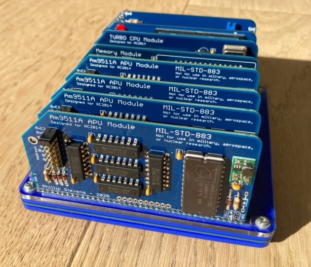
4x Am9511A APU Modules with Z80 CPU.

What is even more perfect is that the APU Module can be scaled for efficient parallel processing, something that would never have been contemplated back in the 1970’s.

Yet Another Z180 Project (YAZ180)

I’m thinking about a new project, something a little unusual but still with a rich history of information upon which to base the build. On Tindie, I found the RC2014 project which is a build of a Z80 platform but based on some modern components. That got me thinking. My next project must be a Z80 based project.

Why the Z80? Well, it was at one stage the most used CPU in the world, which leads to the great depth of information and experience available for designs, hardware, and software. Technically, it is advanced enough to avoid the need for a large number of ancillary chips, multiple power supplies, and multi-phase clocking that the 80088080, and other older chips needed, but still it is complex enough that in doing a project I’ll feel like I’m actually building a computer.

This year marks 40 years (yes 40 years, since launch in July 1976) of the Z80, and still as a design and platform it looks like it will continue to be relevant into the future. So rather than building yet-another-ARM project. It looks like I will be marking the 40th anniversary of the Z80 with a new build.

Zilog_Z80

An early Z80, manufactured in June 1976.

What kind of project? The RC2014 project is an interesting starting point. It is quite simple, being a compact and robust implementation of Grant Searle’s 6 Chip Z80 Computer, but provides more resources than most of the 1980’s Z80 projects offer. After looking at some projects others have done, I think that I should aim to build something a little like a “Back to the Future” Z80 project, a DeLorean (which also appeared as a prototype in 1976) with a fusion reactor.

RC2014 Cylon

RC2014 Cylon

As an outcome I’d like the solution to be able to interact with modern interfaces such as I2C, Ethernet, SPI, and USB, with access to a large physical memory space, with great performance, and yet retain the ability to be a single-step-able experimental platform with LED bus indicators. Single stepping is something that you can’t do with an Arduino, and it is a real differentiation.

Whilst it would be attractive to design in some old-school interface devices, like the Am9511A APU or a Super I/O device, in light of today’s environment the wouldn’t contribute very much to the outcome. So the focus will be squarely on modern I/O.

Also, there is a temptation to build a CP/M system with full disk management. But again there are plenty of CP/M systems around. I’d like to build something more  of an embedded platform, that doesn’t require mass storage to run applications. It would be good if most of the basic interfaces could fit on one board, to avoid the need to build address and data bus extension. I think this will simplify the design significantly.

Design process

This is going to be an iterative process. The first step will be to build the RC2014 project, and test that I can program it.

It will be important to learn a little about Z80 assembler. Later, I may modify the RC2014 project platform.

Then, I’ll lay out a through hole prototype with minimal functionality, to test some performance ideas. If they work on through hole, then they’ll work with SMD. Using through hole also allows me to quickly fix logic or wiring errors that would take a new spin with SMD.

Finally, I’ll build a SMD device that miniaturizes the solution, and makes it more robust.

Processor selection

The Z80 has been built continuously for 40 years, and in that time many manufacturers have produced silicon and several clones have been created. The Z80 range been continuously improved through the Hitachi 64180, to the Zilog Z180, and the Zilog Aclaim eZ80 devices. Each increment has integrated more accessory components, and improved the instruction throughput, as well as increased the clock rate.

Looking at the options available, the original Z80 requires logic to get started. So rather than building serial ports and timers, it looks like the Z180 might be the right place to start. So why not go all the way to the eZ80? Well the eZ80 is not dissimilar to an AVR ATmega device, with all of the system components integrated into the one device. Using an eZ80 CPU wouldn’t be like building a computer at all. It would be much more like building an Arduino, and I’ve been there already.

Out of the Z180 options, I would select the Z8S180 (at 33MHz) because it integrates sufficient material to get started (Timers, Interrupts, MMU, & USARTs), and leaves me the option to add complexity as I get going.

Memory selection

A little research on the processor and available memory provides me with some cornerstones for the design. I will use Flash memory for the  program storage, and static RAM for the system memory. Historically, UV erasable PROM and dynamic RAM would have been used. One advantage of static RAM is that the solution is fully single-step-able. Meaning, I’ll be able to watch the address bus and data bus process each instruction as the Program Counter marches along.

The Z180 can address up to 1MB of physical address space, and it makes sense to provide the full physical memory possible. The price of 1MB of SRAM or of 256kB of Flash is almost nothing these days. As the Z80 logical address space is only 64kB, the Z180 has an inbuilt MMU to manage its physical memory to logical memory mapping.

Memory mapping

NOTE 2017 October: The details in the below discussion are no longer accurate. The memory design has moved on substantially, but this discussion remains for information only. Happily, even completely changing the memory mapping can be done with a software reconfiguration of the Memory / IO logic device.

To keep things simple (in hardware), we can use the MMU available in the Z180 to map the physical memory locations on 20 address lines, into logical addresses that suit us. The MMU can map 4kB pages of physical memory into two relocatable logical locations in the Z80 logical address space. These are called the Banked and the Common 1 locations. The Common 0 memory location begins at physical address 0x00000, and continues to the beginning of Banked memory, which then continues to the Common 1 memory address space.

Therefore the hardware (or physical mapping) will show that the 256kB Flash is located from 0x00000 to 0x3FFFF, and the 1MB RAM from 0x00000 to 0xFFFFF but the lower quarter of the RAM address space mostly masked by Flash. For programming we’ll have to move this around.

When the Z80 starts up it always begins from physical and logical address 0x0000. Therefore it is typical to put the program storage in the lower address range, and the RAM in the upper range. Given the use of the MMU available in the Z180 we initially can map the SRAM into the upper 32kB of logical address space, using the Common 1 bank and CBAR setting, leaving the first 32kB of Flash in the lower address range.

One difficulty is that there are only 3 memory spaces available, so if we want to have a C stack, global buffers and queues, and global data, then we need to put some SRAM in the Common 0 address space. Let’s uncover 8kB of 1MB SRAM and place this from 0x2000 to 0x3fff to provide this C stack and global variable data frame.

At some stage I assume I’ll want to use all of the additional Flash and SRAM available, so I’ll have to integrate programming for MMU bank switching, and RAM heap/stack switching when the need arises. At least initially there will be a statically programmable range of between 8kB Flash with 56kB SRAM to 56kB Flash with 8kB SRAM available within the logical address space, depending on the MMU initialisation settings.

To program the Z180 with a soft programmer, the physical memory addresses will need to be juggled around (glue logic) to disable the Flash and SRAM from appearing in the first 8kB Bytes of the address space. The USB soft programmer will provide program codes in the form of a remote boot-loader to load the contents of programs into the Flash, by moving the entire physical flash through a 4kB or 8kB Banked page. SRAM located in the lower 32kB address range will be loaded with a program to enable buffering and page writing of the desired programs.

Physical Address Range Run Mode Programming Mode
$00000 – $01FFF Flash (8,192B of 256kB) USB (8,192B)
$02000 – $03FFF SRAM (8,192B of 1MB) SRAM (516,096B of 1MB)
$04000 – $3FFFF Flash (245,760B of 256kB)
$40000 – $7FFFF  SRAM (768kB of 1MB)
$80000 – $BFFFF Flash (256kB of 256kB)
$C0000 – $FFFFF SRAM (256kB of 1MB)
Logical Address Range Run Mode Programming Mode
$0000 – $1FFF Flash (8,192B, Common 0) USB (8,192B)
$2000 – $3FFF SRAM (8,192B, Common 0) SRAM (24,576B, Common 0)
$4000 – $5FFF Flash (8,192B, Common 0)
$6000 – $7FFF Flash (8,192B, Banked)
$8000 – $FFFF SRAM (32,768B, Common 1) Flash (32,768B, Banked)

The programming mode (address mapping) will be entered by either a button press, or by signalling from the USB – USART interface lines. The process is to invert the Address 19 line, shifting the physical address location of Flash, and mute Address 0-12 to prevent memory being read from these locations, which allows the USB – USART FIFO to provide program opcodes. Mute by disabling the CE on both Flash and SRAM when A13 through A19 are 0. Then configure the MMU to bring the Flash into Banked logical addresses, using the SRAM to buffer 4kB page writes to Flash memory.

Using the ATMEL WinCUPL tool, it is pretty straightforward to convert the above memory mapping and below logic mapping in CUPL language description to JEDEC format that can be handled by a MiniPro TL866 EEPROM & PLD Programming tool, and programmed into an ATF16V8C  or Lattice GAL16V8D device.

MEMORY_PLD_A

CUPL Memory / IO Definitions

MEMORY_PLD_B

CUPL Memory / IO Decoding

This memory and IO mapping needs to be augmented by a secondary logic mapping for managing programming, single step, and other functions, which will be programmed into a second ATF16V8C or GAL16V8D device. The logic mapping will allow automatic programming initiation via the FT245R USB interface.

LOGIC_PLD_A

CUPL Logic Definitions

LOGIC_PLD_B

CUPL Logic Decoding

Using EEPLD devices will save significant PCB real estate, and will allow me to compensate for minor logic errors after the fact.

screenshot-from-2017-01-28-20-06-10

Schematic for Memory GAL

yaz180-logic-schematic

Schematic for Logic GAL

FCPU selection

The best Flash memory we can get easily is 55ns timing. This is bettered by SRAM, with 45ns access timing. By converting this timing to a bus frequency we can achieve 20MHz or slightly better, but allowing for some buffering or address logic delay it would be better to keep the system bus under the equivalent of 20MHz.

Using this system bus speed of approximately 20MHz then poses a question; which is the right speed? Some references point out that the Z180 is very poor at holding the correct USART rate when the CPU clock is not a magic multiple of the USART rate. This is the same issue that the AVR ATmega device faces when its USART is not driven by a magic frequency clock. Therefore, lets us set  the CPU crystal oscillator to 18.432MHz, being most appropriate magic frequency for the following design.

The Z180 system clock (or PHI) can be double, equivalent, or half the rate of the crystal oscillator base rate. Starting with 18.432MHZ oscillator clock, depending on the CPU Control Register (CCR), the system bus clock (PHI) can be halved and is operated at 9.216MHz. This is slow enough to allow most peripherals to interact with the CPU. Internally, the system bus clock (PHI) can be doubled to operate the CPU at 36.864MHz, by setting both the Clock Multiplier Register (CMR) and the CCR. This rate is slightly overclocking the Z180, but that’s what we live for. We don’t build slow computers.

As we are using 45ns SRAM and 55ns Flash, we will have to insert either 1 or 2 memory wait states when operating at 36.864MHz. This is unavoidable, because of the access speed of both memory devices. Faster SRAM may be available, but faster Flash is quite hard to obtain.

I/O Mapping

I have been thinking about the whole idea of system modularity. Actually, I don’t think the traditional method of building a backplane is such a good idea for what I want to achieve. Extending the address bus a long distance means that I’ll be investing in design and timing issues, that I’m not really sure I know how to solve. So, let’s focus on a smaller design, with on just one board for the time being.

As a computer always needs to be extended and interact with the real world, I think it would be good to add modern user interfaces to the solution. Use Address 15-13 to provide I/O selection options on the CPU Board, using the remaining output pins from the Memory ATF16V8C or GAL16V8D. This will allow flexibility to latch data into the Hex Display, or trigger breakpoints using #M1 and #Wait to allow Single Step execution from any code point.

I/O Address Range Chip Select (A15,A14,A13) Device
$0000 – $1FFF DO NOT USE ($0, b000) Internal I/O
A7-A0
Internal INT
$0000 – $00FF Registers
$2000 – $3FFF BREAK ($1, b001) Break Point Toggle Single Step Mode
$4000 – $5FFF #DIO_CS ($2, b010) PIO 82C55
A1-A0
$4000 – $4003 Registers
$6000 – $7FFF EXPANSION ($3, b011) Hold for Expansion
$8000 – $9FFF #I2C_CS2 ($4, b100) PCA9665
A1-A0
#INT2
$8000 – $8003 Registers
$A000 – $BFFF #I2C_CS1 ($5, b101) PCA9665
A1-A0
#INT1
$A000 – $A003 Registers
$C000 – $DFFF #APU_CS ($6, b110) APU_CS – Am9511A-1
A0 & #WAIT
#INT0
$C000 – $C001 Registers
$E000 – $FFFF EXPANSION ($7, b111) Hold for Expansion

Included I/O features & BOM

CPU

SRAM

Flash

Single Step – The Z-80’s #M1 pin is useful for building logic to single-instruction step the machine. You do this using the memory ready signal on #M1 to clear a 7474 flip-flop, which is clocked by a Single Step signal, to produce a #WAIT signal for the CPU. That stops the machine on the opcode fetch cycle with the address showing on the address bus and the opcode byte showing on the data bus. To move the machine ahead, you clock the flip-flop which releases the #WAIT signal, until the next #M1 clears the 7474  again.

Reset

Memory & Addressing Logic Glue

  • Programmable Logic PLD – Digikey ATF16V8B

USB – Flash programming interface

  • USB-Parallel Bus FTDI245RQ
    Note that  the Write strobe is confusing, but assume ACTIVE LOW.

USB – USART interface

  • USB-Serial FTDI232RQ

Hex 7 Segment Display – 5x Address Digits – 2x Data Digits

  • Decoder DM9368 – Digikey DM9368N-ND
  • LED Display VDMY10C0 & VDMG10C0 – Digikey VDMY10C0TR-ND
  • OR
  • LED Display with Decoder TIL311A – eBay only.

General Digital Input / Output – Being able to read and write simple digital levels is an important thing. So let’s include the 82c55 PIO device.

  • Intel CMOS 82C55 Programmable IO CP82C55A – Digikey CS82C55AZ-ND

I2C interface – This is the most important interface, which provides many extension options, and a plethora of Grove System sensors. Unfortunately the 5V nature of the system precludes using the newest really fast, deep buffer, devices with multiple bus I2C 1MHz bus interfaces, so provide 2x devices to support different applications (eg. video output and sensor acquisition on separate buses). Use the #INT1 & #INT2 interrupts.

Arithmetic Processor Unit – This lovely old chip is now also 40 years old, and was the world’s first APU (or FPU). Potentially, it is too slow to contribute, but still we’ll build it in. Need to provide a 3MHz clock to drive it (FAPU = FCPU/6), and connect its #PAUSE to #WAIT. #END connected to #INT0. RESET is ACTIVE HIGH.

AM9511A-1DC

Am9551A-1 3MHz APU

Bus interface

  • Address & Control – Octal Buffer Driver sn74abt541b – Digikey 296-14668-1-ND
  • Data – Octal Bus Transceiver sn74abth245 – Digikey 296-4140-1-ND

Power Supplies

Excluded I/O features & BOM

Ethernet – Wiznet W5300 Direct address mode requires 3FF of address space. Configure the #INT0 interrupt and implement the DMAC1 I/O to move packets quickly. Exclude this from the initial build, as it is quite a complicated 100 pin device, and it needs 3.3V supply.

USB & SPI interface – provide mass storage capability using either USB or SPI interface devices. The CH37x series is not very well documented, or readily available. There are other options for I2C-SPI bridging which can provide an SPI interface if needed.

  • CH376S – Incorporating the USB functions as described in CH375, and CH372

ADC interface – Better, higher resolution, faster chips are available with I2C interfaces.

  • 8 bit ADC with internal reference MAX158 – Digikey MAX158ACPI+-ND

Video Interface – Can be done using an external I2C device.

  • LCD Video – via I2C with a FTDI EVE

Super I/O – Floppy Disk & IDE Controller – Too hard and doesn’t bring much value to the table. Floppy drives are hard to find, and there are already 2x USART ports available on the Z8S180.

Software & References

Z80 Info

z88dk Development Kit

Small Device C Compiler

SASM Softools – Z180 (MMU aware) C compiler. Commercial Licence.

Programming the Z80 by Rodnay Zaks

The Undocumented Z80

Logic Families

FreeRTOS 9.0.0 for eZ80

Hardware Design notes

Well quite a few iterations on my aspirations and thoughts have resulted in a YAZ180_v1 schematic, that I think is now basically frozen. Some of my design decisions follow.

After deciding not to use the TIL311 LED display devices because they are not easily obtainable, I found the alternative solution using the DM9368 display driver chip and LED display devices was very consuming of space on the board. Since the board had to be no greater than a maximum of 10cm by 16cm to fit within the constraints of my Eagle Hobby licence, I decided to buy some TIL311 devices in advance, and then with the comfort of stock in hand I could use them for the design. Also, they add significantly to the retro-chique.

I would have loved to add the Wiznet W5300 device to the design to provide high speed Ethernet capability, but with a 100 pin VLSI it was just too complicated for the initial design. Next time.

I added a 82c55 interface chip. Knowing that it is very slow, requiring 2 wait states to drive it, is one thing. But the advantage of having multiple latch-able input and output ports, off one fairly compact integrated device made up for that problem. As it is a 1970s device it is also retro-chique accretive.

Designing using CUPL and the Atmel or Lattice PLDs is in my opinion much simpler than tracing schematics and thinking through 7400 series NOR, NAND gates to get the desired addressing logic. Writing the logic in “c” like syntax is much less taxing on the brain.

After deciding to implement no bus drivers, and then building a solution adding drivers and termination to every address and data line, I have rationalised down to bus drivers on data, lower address, and control lines. These are the few lines that appear on all memory and I/O devices, and are taken to every point on the board. The upper address lines only appear on the PLD, SRAM, and Flash, which are very low load modern devices, so there is no point to buffer them. Using ABT logic limits the differential delay on the address lines to 2 ns, and since the read and write select lines are also buffered, there is no issue timing issue created.

And here is the first schematic, in pdf YAZ180_V1. Errors and omissions did occur.

Hardware Layout notes

With the first major layout session behind me, I have the following notes.

Address&DataRouted

Address & Data to SRAM and FLASH

Change the SN74ABT244 for the SN74ABT541. The only difference is the pin ordering, with the 244 being optimal for counter-flowing signals, and the 541 being optimal for unidirectional signals (physically). This will help layout.

Getting 20 address lines and 8 data lines to appear on the SMD SRAM memory is challenging. I will probably reassign the address lines to suit the Z8S180 pin-out, rather than spending hours untangling the lines. It won’t be too easy to do this with the Flash device, but as it is in a PLCC through-hole socket it comes inherently with “vias” making reaching it half as hard as SMD.

Input pin and I/O pins on Z8S180 include weak latch circuits to prevent excessive current draw by the receiver, if the pin is not externally driven. External pull-up or pull-down resistors should not be less than 15 kOhms to ensure that the resistors can control the state of the latch when power is supplied.

Address&Data

All Address and Data lines routed.

afewmoreairwires

A few more air-wires remain, that will need thought.

Following about 10 hours of juggling, just two wires remain together with a plan to resolve them tomorrow.

twoairwires

Just two air-wires remain.

Finished, except for the detailed checking, which usually results in some changes. But, it is done.

The screen grabs below show with the Vcc Layer in Grey, and GND Layer in Green. I have added some basic traces on those layers to close off the routing, which are misleading. The layers are actually completely filled, normally.

This slideshow requires JavaScript.

Bill of Materials

Well, building this retro-computing machine is not quite as cheap as an ATMEL micro-controller board. But then again, it is not quite in the same league, with 1MB of RAM, and 256kB of Flash storage, together with an APU and 9 digits of LED display.

I have ordered all of the components, except the Am9511A-1 APU and the TIL311 LED display devices, from Digikey. The BOM is detailed in this link. To add to BOM, this there are the Am9511A-1 and the TIL311 devices which can be found on eBay or other auction sites.

CoL3S3MUkAAksZ5

And, the PCB looks great!

Bringing up the Prototype

The build and bringing up of the board will continue, once I get the new SMD oven sorted out.

Well, the board has been soldered, and everything looks good. The SMD oven wasn’t as useful as I thought. It turns out that I can solder the fine pitch of the SRAM and FTDI devices fairly well with a normal soldering iron.

My PLD programmer won’t work with ATMEL devices, so I’ve been waiting so long for some Lattice GAL devices to be shipped to me. Over 8 weeks in transit. Finally they’ve landed. So I soldered the rest of the board together.

I’ll have to debug my CUPL programming of the GALs to get everything working, but at least there’s no “magic smoke”.

The TIL311 LEDs are very hot, because they draw so much current. LEDs really have come a long way in efficiency over the past 30 years.

Update 9 Jan 2017. Using this Github Repo, I’ve successfully sent characters to the ASCI. It lives!

Update Friday, January 13th 2017. Initial RAM testing passed!

And now based on this testing, I’ve been able to get the ASCI0 (and ASCI1) working, so that I have NASCOM BASIC Ver 4.7 (1978) running on my 2016 designed computer!

This is a Mandelbrot program running in NASCOM Basic v4.7.

yaz180-glow

Glowing, in a dark  room.

Three major items remain to complete, before a PCB revision.
  • Completing the “in circuit programming” tools, to programme the Flash memory without removing it.
  • Writing drivers for the Intel 82C55 PIO device.
  • Writing drivers for the AMD Am9511A APU device.
Following the PCB revision, I’ll work on the I2C platform, and its drivers.

Next up, programming Flash memory using the FTDI FT245 USB-Parallel port. This was working, but some bad soldering made the on-board FT245 inoperable. Testing was completed using an external device.

Testing for the 82C55 PIO device is now done. It can do a lot more than this, but the proof of life is completed. Time to move on.

Update February 20, 2017. Despite initial misgivings, that the Am9511A APU was wired incorrectly, the proof of life for the APU is now done.

For a long time, I could see that the APU was trying, but just wasn’t making it. Two issues were involved.

Firstly, all of the datasheets assume 74 logic is being used to create the chip select from 3 to 8 address decoding, or similar solutions. What they don’t point out is that the Am9511A  APU chip select MUST be generated from the address lines, because the Z80 (Z180) IORQ line has incorrect timing to drive the Am9511A. The Am9511A needs an 30ns of chip select and address validity after WR is raised, which the Z80 IORQ timing doesn’t provide. Having infinite logic in a GAL available, I had (incorrectly) included the IORQ line in the APU_CS logic. Whilst I’d recognised the issue, it took three lines in an obscure 1981 PhD dissertation to focus the spotlight of clarity. Thank you Mr Haining.

Secondly, the Am9511A samples I have on hand won’t work at 3.072MHz. I guess they were cutting very close to the limit in the day.

img_0626

YAZ180 v1 full configuration.

I’ve finished an initial revision of the PCB to fix all of the known errata. I’ll sit on it a bit until I can double check that everything is good.

Errata

The power supply section was done very simply in the V1 build. I underestimated the requirement for 5V power, thinking that 1A should be sufficient. Before I built the V1 board I realised my error and replaced the 5V 1A regulator with a AP1506 that can supply 3A. I also changed the inductor to a lower inductance and higher current version.

I’ve now revised the power supply  section to use LM2596 3A device for the 5V supply, as this device has a larger input voltage range (up to 40V) , and I have inserted thermal vias to improve the heat spreading into the back side of the board.

The 12V supply only needs to provide about 90mA for the APU. I’ve reduced the capacity of the regulator down to 500mA, and have saved some space by using a LM2674 in SOIC-8 format. Whilst the Am9511A gets uncomfortably warm, the power supply doesn’t.

Also, I simply forgot to provide a 3.3V supply, that is required for the I2C interface devices. So this has been repaired with a 1117 linear regulator, supplied by the 5V regulator. It is the same device I used in the Goldilocks Analogue as I have some parts in hand.

I’ve swapped the USB connectors to male versions. Can’t understand why I built YAZ180 V1 with female connectors. Just silly.

I’ve swapped the location of the RESET and SINGLE_STEP buttons. It makes more sense to have the buttons doing the same function closer together.

The Z8S180 requires that its DCD0 be held low, before the USART0 can transmit. This pin is now tied to GND.

The Logic GAL device, in Registered Mode, requires to have its OE held low. This pin is now tied to GND.

To generate a RESET signal, the reset request input to the Logic GAL can’t be on Pin1 in Registered Mode, so the RESET_REQ signal was moved to Pin14. Pin1 in Registered Mode is connected exclusively to the CLK for the GAL flip-flops. In order to clock the flip-flop implemented in the YAZ180 programming mode logic, the RESET line was connected to Pin1.

The Am9511A-1 although specified at 3MHz, doesn’t pass tests at 3.072MHz. So it will have to be de-rated to 1:8 from the Z8S180 system clock. This takes the clock speed down to 2.304MHz. The clock divider chip will be replaced by a sn74ls93 from Digikey 296-3749-5-ND.

For the purposes of enjoyment, I’ve connected the Z8S180 DMA engine DREQ1 and TEND1 lines to the Am9511A SVREQ and SVACK lines. The SVREQ requires a NOT to generate the inverted Z8S180 signal for DREQ1. Although there are very few bytes loaded into the Am9511A, this should allow them to be written by the DMA engine.

Both AMD Am9511A and Intel 82C55 need the address and chip select lines to remain valid for a period after the RD or WR signal has gone high. Therefore we need to remove the existence of a valid IORQ signal from the calculation of their select line, and just rely purely on their address decoding (and absence of MREQ). The CUPL coding has been adjusted

The Am9511A supports 1 I/O Wait State, as RD & WR to Pause is 100ns. The 82C55 requires 2 I/O Wait states, as RD is 200ns minimum.

Update February 24th.

The new PCB has been ordered.

I’ll start a new post for the YAZ180 V2 when the PCB is back from manufacturing.