
So I soldered it all together, and it doesn’t work. Typical. It looked so easy, all of the instructions are straightforward, and the boards are clear and labeled for easy assembly.
I guess this is the story for many projects and some of them never proceed past this point and end up in the junk box. But, sometimes there’s a guide for what to do when there’s trouble.
So this is my guide to how I fixed my RC2014.
1. Power supply
I installed a 7405 linear regulator into the provided slot on the backplane. Because there was no space for a protection diode I added one in series to the power input terminal. First, remove all of the cards from the backplane. We’ll start with power supplies. Using a 12V supply, let’s check that there is 5V and GND available to every backplane slot.
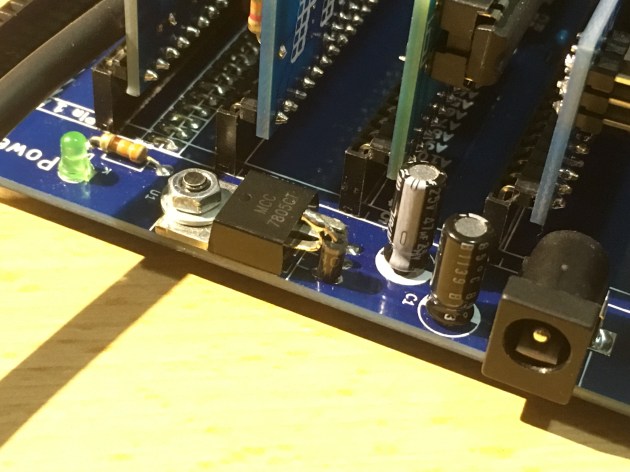
7805 Regulator with 1A linear diode in Vin.
2. Reset
I have used the new backplane Reset function. Let’s test that it is effective in providing 5V pull up normally, and pull down to GND when the reset button is depressed.
3.Clock Function
The CPU requires a Clock, and that is provided by the small PCB containing the crystal and the buffer amplifiers. I didn’t equip the Reset button or resistor on my build, because 2x resistors is not required, and only one switch was included in the materials provided.
Using an oscilloscope to watch the signal, the performance of the Clock and its crystal can be measured. So the crystal is oscillating and produces 7.353MHz with a good strong signal. And it is available across the backplane to all the slots.
[Add picture later. I’ve lost the USB stick.]
4. CPU General
Insert the CPU module and check that it has 5V power, GND, and the Clock and Reset lines are working as expected.
On the Address lines, there should be a signal at 1.232 MHz, representing the cycle of CPU running NOPs. With this signal in place, we can move on to the ROM and RAM modules.
[Add picture later, I’ve lost the USB stick.]
5. ROM & RAM
Now we check that there is power and ground at both of the ROM and RAM modules. If that is the case then it is back to the logic analyser to check what is happening on the system now that the CPU has access to instructions to read.
6. Logic Analyser
With an 8 input logic analyser we can’t look at all of the signals at one time, so let’s choose some relevant ones. The lower few address lines are interesting, because they show where the CPU is reading instructions as it starts up. Also, if the Serial I/O port is attached then the Tx and Rx lines can be monitored on the backplane too.
Reset the system to see what happens immediately after the Reset is released. Note the ASCII text message appearing on the Tx line on the backplane, noting the Geoff Seale copywrite, the invitation to choose cold or warm boot, and the memory size. This means that the RC2014 is living, but somehow the Serial I/O board is not functioning properly. So we need to focus attention there.
7. Serial I/O
The Serial I/O card should be connected to the FTDI Basic or other FTDI FT232R equivalent device. As I had a PL2303 based serial cable, I decided to use that, as it is much cleaner than using an FTDI adapter, and it allows the Serial I/O board to be positioned anywhere on the backplane.
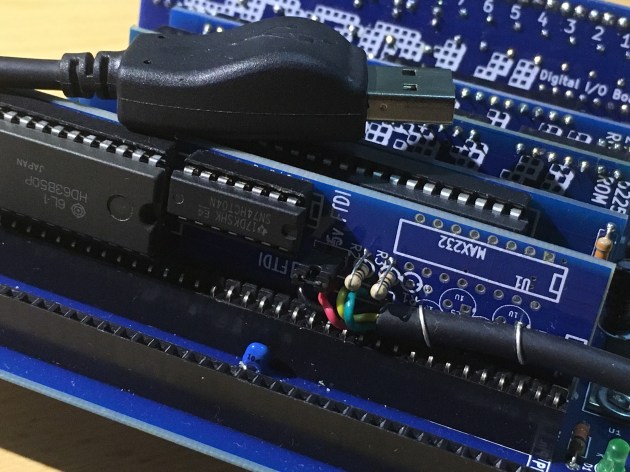
Prologic PL2303 Serial Cable, exits inline with backplane connector.
The Logic Analyser shows that the 63B50P chip is doing its job and producing characters on the Tx line. But we aren’t seeing characters on the FTDI Rx line on the Terminal. That is a problem. Note that there are 2.2kOhm resistors in series with the serial module Rx and Tx lines. That’s a bit more than I’d expect to see. Let’s reduce those resistors down to around 100 Ohm. They could be 0 Ohm, but it is better to be a bit conservative.
Reducing the in series resistance doesn’t allow either the FTDI or the Prologic interface to work either. There’s something else going on here.
With both the Logic Analyser and the FTDI interface attached to the RC2014 the comforting welcome from Greg Searle appears on the Terminal, urging us to cold or warm boot. Yet, when the logic analyser is removed the serial I/O is no longer working.
This looks like some kind of ground loop problem. I don’t know how this can be fixed easily. The RC2014 device only works when there is a ground provided by another source, such as the Logic Analyser.
8. Other issues
The Serial I/O device was delivered one incorrect IC socket (14 pin instead of 16 pin), so I had to solder one chip directly to the board. Not a big issue.
There is no mention of how the ROM system needs to be configured. There are three options available for selection. The right one is with all of the address lines set to 0.
The basic program is described on Greg Searle’s Simple Z80 web page. There is little mention that this this is where to go for additional software support and programming assistance.
Anyway, with the caviet that the device has to be connected with an external earth, the RC2014 is working perfectly.
9. Earth Issues
After asking Spencer for some ideas, and doing some further circuit testing, I found that I had somehow damaged the ground wire near the centre of the backplane. That was allowing the RC2014 to function when GND was provided by both FTDI and Logic Analyser on opposite sides of the backplane, but to fail when only one GND was provided.
I resolved this by soldering an additional wire along the entire GND line. Whilst I could have just bridged the gap, I preferred to improve the GND stability by adding conductor all along its length. I covered the wire with hot-glue to increase its stability. As a side effect it adds a non-slip characteristic to the backplane, and helps to protect my desk from being scratched.
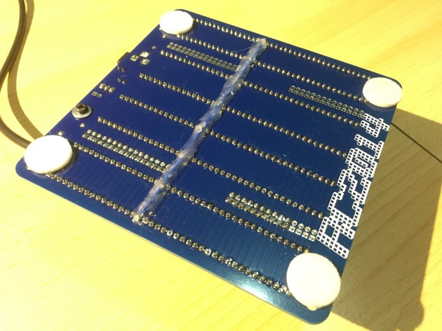
GND wire hidden under a protective hot glue sheath.
Now that I’ve fixed my dodgy soldering on the GND line, everything is much better, and works perfectly
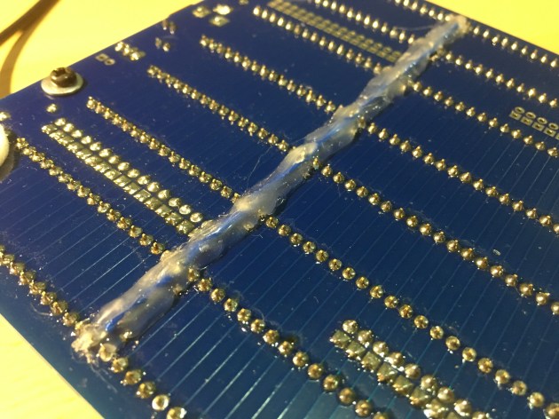
The hot glue sheath helps to hold the solder pins off my desk too. Integrated non-slip.

Pingback: Z80 C code development with Eclipse and z88dk | feilipu
Interesting. Thank you. Don’t forget your images…