Yet Another Z180 (YAZ180 v2)

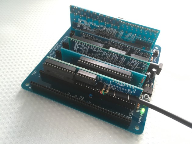
Testing on the YAZ180 v1 , shown below, is now complete. I don’t want to use it for further driver and platform development, because the PLCC socket for the 256kB Flash is becoming worn-out.

It will continue to operate as an augmented Nascom Basic machine, with an integrated Intel HEX loader (HexLoadr) supporting direct loaded assembler or C applications.

img_0626

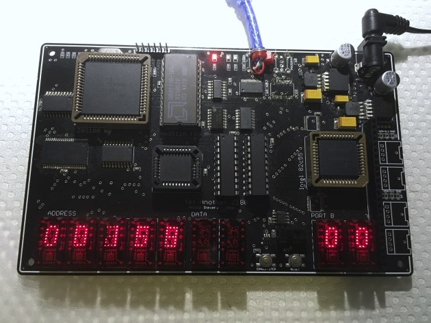
YAZ180 v1 at full configuration.

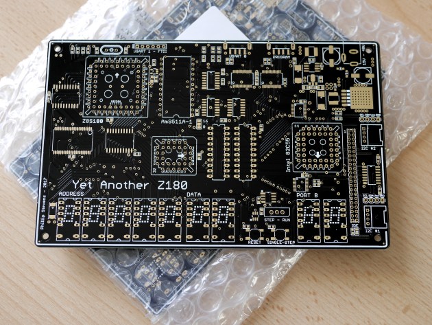
The new PCB for the YAZ180 v2 has been ordered.

These are some screenshots of the new PCB.


Update

Pi Day, March 14 2017.

After dwelling on the fact that the V2 PCB was really just a clean up the V1 PCB, with no additional features, I decided not to build the beautiful new PCBs that arrived today.

But rather, to create a new PCB with additional features.


New Features

When I originally designed the YAZ180 the breakout for the 82C55 was simply an interim design, to enable me to test the board. I was thinking of making an Arduino style pin-out, or something along those lines. But this is something much better.

Recently, after reading Paul’s page on interfacing an IDE drive to an 8051 microprocessor with the 82C55, I decided that adding IDE to the YAZ180 was a must-have feature.

So there is a new connector on the YAZ180 to break out the 82C55 pins, in IDE 44-pin 2mm format. I have not followed the design provided by Paul exactly. I’d note that his design and the earlier design by Peter Fraasse were specialist designs, which don’t support the generalised usage of the 82C55 chip, beyond the IDE functionality.

By the above statement I mean that in Mode 1 and Mode 2 for Port A and Port B, the PC2, PC4, and PC6 pins of the 82C55 device are designated registered strobe input pins /STB in input mode, or peripheral acknowledge /ACK in output mode. If an inverting output buffer is connected on these lines, then the registered input and output mode capability is lost. This would restrict the functionality of the 82C55 to simply Mode 0, being the mode that is used to create the IDE functionality.

As I’ve connected the three IDE address selection pins to PC2, PC4, and PC6, and these pins are not passed through an inverting buffer in the design, it is possible to use the 82C55 in any of its modes, and therefore to use the IDE 2.5″ 44-pin form factor to connect the YAZ180 82C55 ports to extension PCBs of any type or design.

As a connected IDE drive or other extension board may need to interrupt the CPU, I have connected the IDE INTRQ pin to the remaining inverting buffer to provide an input to the CPU on /INT0. As the /INT0 (or actually the INTRQ) input terminates on the IDE header, either a IDE drive through INTRQ, or either of the two 82C55 INTR pins, PC3 or PC0, can originate the interrupt.

I have reconfigured the Am9511A-1 to use the /NMI interrupt, as previously the /INT0 was configured.

The new YAZ180 v2 PCB has been ordered. YAZ180_v2_Schematic.

Happy Pi Day.

Update – RetroChallenge Day 1

I’ve decided to enter the RetroChallenge 2017/04 and my challenge is to read and write to an IDE drive using the newly configured IDE interface on the YAZ180v2. But before I can write the code for the IDE interface, there’s a bit of building and testing that needs to be done.

The new PCBs arrived a few days ago, and they look great. But Arduino Day and the first day of the RetroChallenge 2017/04, 1st April, seemed like a good day to lay them out.

P1080754

New PCBs. 2oz Copper, 2mm thick. Opulent.

I was hoping to lay build several boards at once, but somehow I forgot that there was only one RAM and one FT245 device in my component stocks. That means that I had to satisfy myself with just one board for now.

Note the suitably Retro PowerMac (circa 2001) driving the layout guide screen.
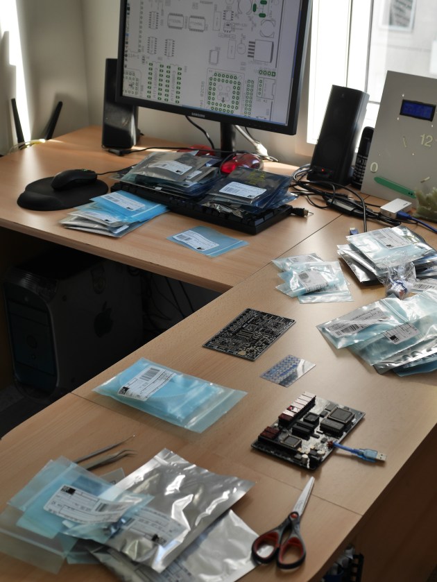
P1080755

Adhoc Workspace

This is the board just before cooking. Respect to anyone who notices the substantial noob layout mistake. Anyway, after a small smokey explosion, everything was rectified.

P1080758

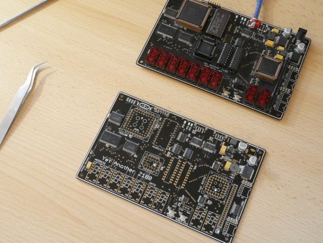
Two YAZ180 versions, side by side.

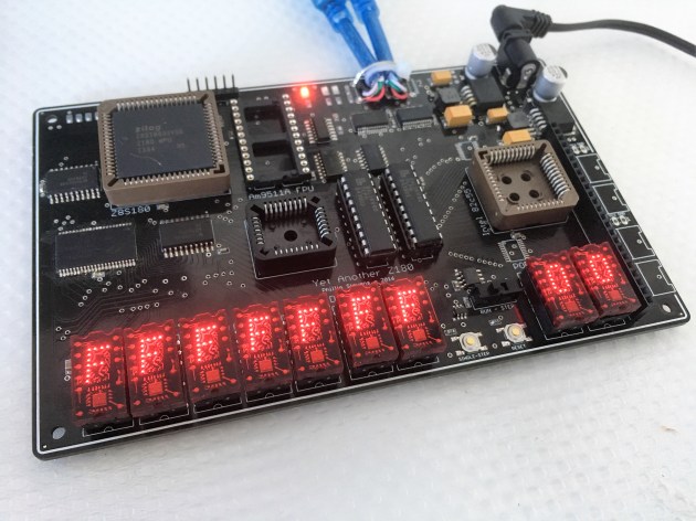
This is the finished build of the YAZ180 v2. Looks very tasty. Retro goodness.

P1080761.JPG

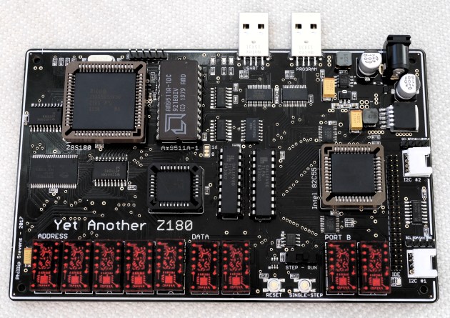
Fully populated YAZ180 v2 PCB.

I’m still working on fixing an issue with my code, which I noticed when experimenting with the Am9511A APU, and inserting an Interrupt Jump Table. Basically, I’m getting jumps to odd or  random locations, which is detected buy filling unused locations with 0x76, the HALT, OpCode. The most common address where the HALT is executed at is 0x00C3.

Previously, I’d been filling unused locations with 0xFF, the RST 38H OpCode shared with the INT0 location 0x0038, which was causing the APU to be triggered inappropriately. This issue has me snookered. I can’t move on, in the software sense, until it is resolved .


This slideshow requires JavaScript.

Update – RetroChallenge Day 8

Well this week was one of the most frustrating weeks ever, in terms of time spent vs. results obtained.

There are two major projects in hand. 1. Getting the YAZ180 v2 running, and 2. resolving the software issue plaguing my initialisation code.

Hardware issues

Bringing up a new piece of hardware is never easy. Initially, nothing can be trusted to work, and everything needs to be checked against the design, and then even the design checked for correctness. Bringing up the YAZ180 v1 was very time consuming, because I had to develop the PLD design during the process, as well as checking that all the hardware was sorking as it should. I thought that bringing up the YAZ180 v2 would be easy. Just solder it together and win. But it has not been so simple.

Essentially, after a week of working on this every evening, I don’t know why it is not working correctly. All the standard things, volts, clock, stuck address and data lines, etc are all working correctly. But it still doesn’t work. And, it may not be just one thing that is wrong, but if anything is not perfect it just won’t work.

After a few days of testing, I found that I’d programmed the PLD devices with an old version of the CUPL code. Nearly right, but not exactly right. Once I’d isolated that issue, by ensuring the new GAL devices worked perfectly in the V1 board, I thought it would be enough. But no. There’s still something wrong.

My current thought is that somehow, either electro-static damage or heat damage, the RAM is unreliable. But, I’m not sure enough of this to unsolder the RAM device and replace it. I’ll be spending this weekend on resolving this problem.

Software issues

Because of the effort I’ve been putting into resolving the hardware issues, I’ve not been able to solve the software issue apparent in the YAZ180 initialisation and serial code. I’ve documented the issue on Github.

My lesson learned is NOT to fill unused memory with 0xFF bytes. This causes RST 38H jumps to the INT0 location when the PC is incorrectly loaded, and can be very distracting. Best to fill unused memory with either 0x76 HALT bytes, to see where things became broken, or with 0xC9 RET bytes to just float over the underlying issue.

I’ll need to fix this properly, but it has consumed several weeks of effort, and I’m not much closer to resolution.

Update – RetroChallenge Day 10

The weekend was unkind, but today some new eyes (literally) have brought successes.

Hardware Issues

After doing quite a bit of further testing, I’m fairly sure that I’ve damaged the RAM and will need to replace it. So, I’ve ordered a hot-air solder gun. Should have had one for a long time. Finally, I’ve got a round-‘tuit. I’ll have to order some replacement components too, which will result in being able to make additional boards as well.

Software Issues

Finally, I’ve resolved my issue. What we had here was a classic “failure to understand”. Somewhat embarrassed to leave this here for Internet eternity.

  • Z80 vectors are supported by a JUMP table.
  • Z180 vectors are supported by an ADDRESS table.

Insert JP instructions into an address table and you will have a very very bad day.

Or in my case, quite a few of them.

This issue cost so much time. But at least on the up side, I’ve written robust Z80 and Z180 vector tables, improved my ASCI code, and cleaned up initialisation code, in trying to track this down.

Also finally, I now understand. Which is the entire point, anyway.

Update – RetroChallenge Day 17

Following up on the success of last weekend, I was hoping to have a lot of achievement to write about today. Unfortunately, it has been a grind this week too.

I have been distracted back into the original project that unearthed my previous software problem, and led me along the path to getting a much better understanding of the Z180 CPU, and then solving the issue. The original project was building an interrupt driven driver for the Am9511A-1 Arithmetic Processing Unit.

I’ve spent pretty much the past week on this code, and digging through it with a fine tooth comb. I’m now of a belief that my Am9511A driver code is correct, but my hardware is not correct and may never be correct.

The issue lies with the requirement for the Am9511A to have the Address lines and Chip Select signal remain valid for 30ns following raising of the Write signal. Unfortunately, the Z180 only maintains valid address lines for 5ns following Write. This means that writing to the AM9511A APU is very much a hit and miss affair, with miss being the most likely outcome. I’m still thinking about ways to bodge this to work. But, I think that it may just be too hard to get the old APU to work with a modern CPU. More on this later.

This week I’ll be working on the PaulMon IDE code, and migrating it from 8051 to Z80 nomenclature, and trying to get it to compile.

Update – RetroChallenge Day 21

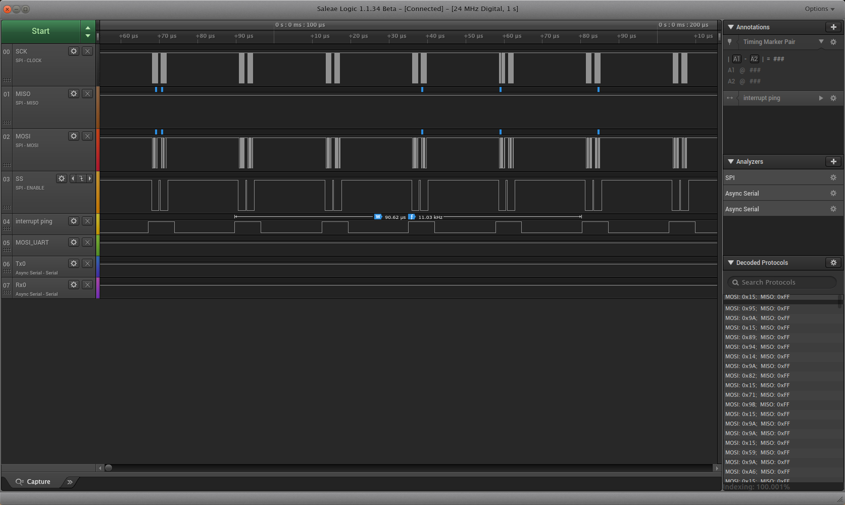
Well the last couple of days have been exciting, as I found a way to make the Am9511A APU work. A hint from a fellow competitor (on working with the MC6809 CPU) inspired me to look further for information on options to fix the hardware interface.

The Z180 E CLOCK

The Z180 has an almost undocumented feature, called the E Clock. Yes, it is documented in datasheet that it exists, but there’s no real background that I can find as to why it exists, except that is for a Secondary Bus Interface. This pin and signal doesn’t exist on the Z80, for example. Anyway, since it has the same name as a signal on the MC6809, I thought it might be worth looking at it. It turns out that the E Clock provides a shortened version of the WR and RD cycles. Which is exactly what we need.

One caveat however, when running at doubled PHI rates (i.e. 1:1 PHI – CLK) the shortening of the E Clock signal is not sufficient to drive the APU successfully. At 18.432MHz, the PHI/2 timing is 27ns. Therefore, the minimum of 30ns between release of WR and CS is not always held. This means that we’ll need to keep the PHI at half CLK whilst using writing data into the APU. In practice this means that using the APU requires we cut the CPU clock by 50% or PHI/2 being 57ns, to ensure the trailing 30ns is provided.

Anyway. Good news. With the revised timing, the Am9511A-1 is working.

Am9511A FDIV

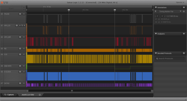
Am9511A APU Floating Divide in 115us

The E Clock is not an inverted signal, so to generate the active low APU_WR signal we have to first invert it, then OR it with the WR signal. For the purposes of testing, I’ve got a little breadboard with a GAL on the side, but later I’ll build a new PCB and add in a SN74LVC1G97 little logic device to provide the APU_WR signal.

Am9511A FDIV PUPI

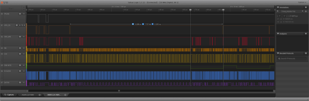
Am9511A APU FDIV PUPI command interval 128us

Am9511A FDIV PHI6 Cycles

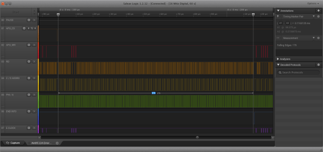
Am9511A APU FDIV in 179 Phi/6 Clock cycles

So now we see the Am9511A APU FDIV floating point divide takes about 101us to 115us when running at 1.536MHz, or from the datasheet 154 to 184 clock cycles. In 101us, the Z180 CPU at 36.864MHz produces 3,723 cycles. To produce a floating point divide using the Lawrence Livermore Library requires about 13,080 cycles, according to the AM9511A Floating Point Processor Manual by Steven Cheng. Therefore, we are still substantially faster than antique software on a modern Z180!

Update – RetroChallenge Wrap Up

Well the month of RC2017/04 didn’t go quite as planned. My original intention was to have the YAZ180v2 working very quickly, then get straight down to porting Paul’s IDE code from 8051 to Z180 to get the new IDE interface working. But, there were several speed bumps along the way.

Gaining an education

Since I just started on this whole Z80 processor and assembly language programming thing a few months ago, I don’t have a long history of coding to fall back on. I had written some code for the Z80 in the RC2014 hardware, which I then tried to use on the Z180 in the YAZ180. But, there is a subtle difference in “generation” between the way the interrupt vectors work across the two machines. Obvious, once you know about it but a real “time killer” if you don’t.

Firstly, filling unused space in your assembly program with 0xFF is a very dangerous thing to do in Z80 assembler, particularly if you don’t understand that 0xFF is the op code for RST38, which is a single byte jump to the same location as the Interrupt 0 in IM1 mode. It would make more sense to fill the unused space with 0x76, which is the HALT instruction, to trap an unexpected program counter value.

Look before you leap

Secondly, the interrupt vectors on the Z80 were designed to contain code, and the PC is just loaded with the address of the vector, and execution begins from there. So for an INT0 (or RST38) execution begins from 0x0038. But, the interrupt vectors on the Z180 are designed to hold an address. The difference being that an interrupt will load the PC with the contents of the two bytes at the vector, and then begin execution from there. I think this difference is a sign of the generational difference between the two implementations. One of the clearest differences I can find, anyway.

Timing is everything

One of the goals for the YAZ180 is to bring some old chips back to life, in a modern platform. Along with the TIL311, GAL16v8, and 82C55 devices, the Am9511A holds pride of place as the very first arithmetic processing unit ever made. I’ve invested far too much time in getting the Am9511A to work, but it is important to me that my project can make it work.

I believed that I had devices that were specified to run at 3MHz but which in fact didn’t. That may be incorrect. More likely was that I wasn’t driving them properly, because my timing was out. I will need to go back and test them all again.

Here the issue is that the Am9511A requires extended validity of data and chip select signal, following the validity of the write signal. At least 30ns is required. This is not provided by the Z180 in its normal timing, although in the configuration I have it, coincidentally because I’d buffered the data bus, it is nearly right. Only the chip select line was being incorrectly handled.

I was nearly giving up but then a tweet from a fellow RC2017/04 competitor gave me the inspiration to look further. It turns out that the Z180 has a secondary I/O timing signal called the E Clock. This signal is not present on the Z80, and as I didn’t understand its purpose I’d left it unconnected in the YAZ180.

Whilst the Zilog datasheets on the Z180 completely gloss over the purpose of the E Clock signal, by simply not mentioning it, the original Hitachi 64180 datasheets do mention it. The original purpose of the E Clock signal was to provide timing for “a large selection of 6800 type peripheral devices” including the “Hitachi 6300 CMOS series (6221 PIA, 6350 ACIA, etc) as well as the 6500 family devices”.

In summary, the E Clock provides a signal that is half a T cycle shorter than the write signal. It means that gating the write signal with the E Clock would allow me to release the APU write signal sufficiently early to maintain the extended chip select timing required. Basically, the APU won’t operate with a Z180 T Cycle any less than 60ns, or 16.6MHz. So in my implementation, the PHI clock will need to run at half speed or 9.234MHz, whilst the Z180 is using the Am9511A. Unless I cook up another plan.

Zapped

And the final note from this month is that I believe my very poor ESD protocol has led to the destruction of the SRAM on my YAZ180v2. Therefore I had to desolder it (and it looked so nicely done) to remove it, and order some new components.

Ordering new components is always a bit of a hurdle for me. I’ve collected quite a few things that I don’t use, so I tend to ration myself on purchases vs. progress. Finally, at the end of the month I ordered more components to build further YAZ180 boards, and some spare SRAM to enable me to repair the one I have made already.

It continues to amaze me just how much difference there is in the cost to build an Arduino AVR board (basically just a chip at the most essential level), vs something like the YAZ180. The YAZ180v2 bill of materials, excluding specials like the GAL16V8D, TIL311, and Am9511A devices that I have to find of eBay, comes to over $150 Australian!!! We need to export more coal, to get the AUD dollar back up there!

And that’s it for my RC2017/04 month. Soon as the parts arrive I’ll be completing the YAZ180v2, and then testing the IDE interface. I hope that will be done before the end of 2017/05.

Update – Post RetroChallenge

Well good news. The only issue was a bad solder joint on the new SRAM chip. Now the YAZ180v2 is running, and I can get onto translating the IDE code from 8051 to Z80.

IMG_0698

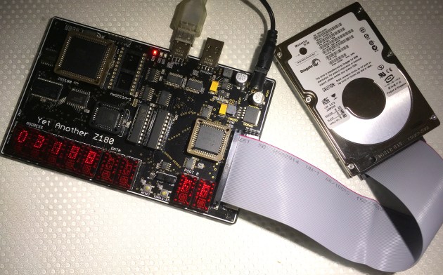
YAZ180 with IDE drive attached.

I’ve sourced code from both PJRC in 8051 mnemonics for an 8255 PIO and from Retroleum in Z80 mnemonics for an 8 bit interface. Between the two of them, together with the examples from the OSDev Wiki, it should be easy to make a fairly robust implementation. And, on May 18th, the driver code was finally working.

Next activity is to integrate this into the z88dk, and then using the FAT-FS code from Elm ChaN, get the disks properly working.

Update – August 2017

Over the past few months progress has been made on various fronts with the YAZ180v2. Firstly, the IDE interface is fully working, and has been integrated into z88dk. Also, the issues with the Am9511A-1 APU have been resolved, and a working driver has been integrated into z88dk. While I still have to revise the C interface for these two pieces of code, because I’m still learning this, the development work is now done.

I am particuarly happy about getting the Am9511A APU working, as this was causing me the most technical difficulty, and stretched my understanding the most. I’m also happy that the capability in the Am9511A seems to be realised through performance improvements in arithmetic computation.

Over the coming months, I hope to resolve the remaining untested components in the YAZ180. These include the parallel programming interface, to allow the YAZ180 to be “cold loaded”, to protect against bricking the system, if a user doesn’t have a EEPROM or Flash writer. I’m still in two minds abou this feature, as the cost of the FT245 device and USB socket is about the same as a stand alone EEPROM writer, and the parallel programming interface consumes space that could be otherwise used for an SPI or USB interface, for example.

I also need to test the I2C interfaces, and debug the driver that I wrote back in May (still unused) to complete the feature set.

With this done, I’ve now done a new minor revision of the hardware, to clean up the issues that have been noted over the past months.

Open Issues

  • APU – Gate E clock with WR to produce shortened APU WR
  • NMI – remove this from the APU, and terminate high. Not CP/M compatible.
  • INTO – reconnect it to the APU.
  • 5V – Power inductor spacing.

Update – October 2017

Well, I fixed the issues and then convinced myself that there needed to be Yet Another feature added to the YAZ180, before I signed it off. So now, the v2.1 board has access to the Internet through an ESP-01S AT interface.


This slideshow requires JavaScript.

I sell on Tindie

Building up this new board will be November and December’s activity, together with building a complete YABIOS (Yet Another BIOS) to make use of all of the features packed into the YAZ180 board. I’ll be picking the best bits, IMHO, from the Cambridge Z88, ZX Spectrum, and CP/M 2.2 – ZSystem to build a banking capable YABIOS, supporting 1MByte of address space.

Update – August 2018

I seriously need to write another blog on the YAZ180. But I guess the Github commits just speak for themselves. There are only three things left on the to-do list. 1. finish the firmware loading program. 2. rewrite the I2C interface. And 3. implement FreeRTOS as a hypervisor allowing multiple 60kB applications to run simultaneously.

Here’s a picture of an application, which was one of the early drivers for building the YAZ180, a mass-storage platform for my HP48 calculator.

IMG_1572

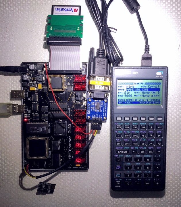
YAZ180 communicating with HP48 using Kermit on ASCI1 (TTY).

Z80 C code development with Eclipse and z88dk

I’m building a Z180 based development board called the YAZ180 for the 40th anniversary of the Z80 processor. As part of that process, I need to have a development environment that supports the Z80 and the Z180 processors. As I haven’t finished building the YAZ180 yet, I’ll be testing the development environment on the RC2014 platform in the interim.

IMG_0084

RC2014 Serial I/O & CPU

There are a couple of major differences in the workflow required to program the YAZ180 from the RC2014. The RC2014 requires an EEPROM programmer to burn the resulting HEX file into its ROM. Eventually, the YAZ180 will use a PERL program to manipulate a parallel port to programme FLASH memory. However, for the purposes of setting up a development environment they are essentially the same.

img_0404

YAZ180 Prototype

To set up the required environment, we’ll need to have:

  • A C compiler suite capable of generating HEX or BIN files for burning onto the hardware.
  • Applicable .CRT files to initialise the CPU and RAM, either Z80 or Z180 specific, so that the C environment can be properly launch.
  • Suitable library files for USART, and other interfaces, appropriate for the hardware in use.
  • Configuration to allow the correct tools and libraries to be found from within the Eclipse IDE.

A C Compiler Suite

There are only a few options for C compilers for the Z80 processor. There is a the Zilog development environment, and the SASM Softools. On the open source side there are two options worth mentioning, being the Small Device C Compiler (SDCC) and the Z88DK Small C Compiler.

There are a few reviews on the Internet of the various options, but in summary the best outcome seems to be to use the Z88DK together with the SDCC Compiler, and the “new library”.

The Z88DK team contributed this information to the RC2014 forum, which gives an overview of the options.

There are two C compilers. One C compiler is sccz80 which is derived from small C but z88dk’s version has seen continuous development over the past 30 years so it’s had most of the limitations of small C removed. For example, floating point is supported, ANSI C declarations are supported, 8/16/32-bit integers are supported and so on. It is a little short of C89 compliance with a few notable non-compliances being multi-dimensional arrays and function pointer prototyping.

The other C compiler is a patch of sdcc, another open source compiler that attempts to implement subsets of C89, C99 and C11. sdcc is an optimizing compiler and z88dk’s patch improves on sdcc’s output by supplying some Z80 bugfixes not yet incorporated into sdcc itself and by supplying a very large set of peephole rules to further improve output.

You can choose which C compiler you use by selecting the appropriate switch on the command line. In your makefile you are using sccz80. To use sdcc, “-clib=sdcc_ix” or “-clib=sdcc_iy” would appear in the compile line.

And then there are two C libraries.

The classic C library is the C library that has always shipped with z88dk. It has many crts available for it that allows compiling for a lot of target machines out of the box. The level of library support varies by target with the best supported having sprite libraries, sound, graphics, etc supplementing the standard c library. It is mostly written in machine code and has a small stdio implementation. However, at this time it cannot be used to generate ROMable code as it mixes variables with code in the output binary. It’s also not compatible with sdcc at this time. Both of these issues are being addressed now.

The new C library is a rewrite from scratch with the intention of meeting a subset of C11 compliance. It is 100% machine code, is written to be compatible with any C compiler, and can generate ROMable code with separation of ROM and RAM data. The stdio model is object oriented and allows device drivers to be written using code inheritance from the library. Although it’s not finished (it’s missing disk io and non-blocking io), it is in an advanced state.

The choice of C library is made on the compile line. “-clib=new”, “-clib=sdcc_ix” and “-clib=sdcc_iy” all use the new C library. Anything else uses the classic C library. In order to generate ROMable code, you should really be using the new C library.

The sdcc_ix and sdcc_iy libraries are chosen when sdcc is the compiler and are selected between by either ”-clib=sdcc_ix” or ”-clib=sdcc_iy” on the compile line. The difference between the two is which index register the C library uses. “sdcc_ix” corresponds to the library using ix and “sdcc_iy” corresponds to the library using iy.

It’s always preferable to use the “sdcc_iy” version of the library because this gives sdcc sole use of ix for its frame pointer while the library uses iy. If “sdcc_ix” is selected, sdcc and the library must share ix which means the library must insert extra code to preserve the ix register when it is used. This means the “sdcc_iy” compile will be smaller.

z88dk’s C library is different from other compilers in that it is written in assembly language, so it is more compact and faster than other z80 C compilers.

Installation instructions for z88dk here and I’d recommend using a nightly build rather than the last release. z88dk is an active project and it changes quite quickly. If you run on windows or mac there are binary packages available from the nightly build. For linux or other targets there are instructions for building from source and for patching sdcc to create zsdcc, z88dk’s version of sdcc.

Just to add for the ROM target: the new C lib allows the stored data section to be lz77 compressed so this should save a few bytes in the stored binary in ROM. Another thing you could do is compile a program for RAM and store a compressed copy in ROM that gets decompressed into RAM at startup.

Z88DK & SDCC Installation

I’m installing Z88DK and SDCC onto Ubuntu 16.04 AMD64 and, since the machine has recently been refreshed, many packages that were required for the install were missing.

Clone the latest nightly checked Z88DK Github package:

git clone https://github.com/z88dk/z88dk.git

sudo apt-get install expect texinfo libxml2-dev flex bison gputils libboost-dev

This will create a populated z88dk directory in the current working directory.

To succeed in building the ‘z80svg’ graphics tool you need the ‘libxml2’ library to be previously installed, although its absence will not prevent the rest of the kit from building.

Then, just type:

cd z88dk
git submodule update --init --recursive
chmod 777 build.sh (just in case)
./build.sh

You can run z88dk keeping it in the current location, all you need to do is to set the following environment variables.

Supposing you have bash (most likely it is your system default shell) and you want to keep z88dk in your home directory, you can configure it permanently in this way:

vi ~/.profile

Modify the configuration by adding these lines (with the appropriate paths).

export PATH=${PATH}:${HOME}/z88dk/bin
export ZCCCFG=${HOME}/z88dk/lib/config

A system install is not supported in this release of Z88DK.

Then to install the SDCC compiled specifically for the Z80 and Z180 these are the instructions.

Check out the current development version of sdcc. If you already have the sdcc-code tree available from a previous checkout you can instead perform an update.

svn checkout svn://svn.code.sf.net/p/sdcc/code/trunk@14210 sdcc-code
# or if you're doing this to refresh your sdcc installation...
cd sdcc-code
svn update -r 14210

You will have to apply the svn patch found in sdcc_z88dk_patch.zip and build sdcc from source. Copy “sdcc-z88dk.patch” from inside sdcc_z88dk_patch.zip into the sdcc-code directory.

The supplied configuration options disables all ports other than the Z80 family ports, and turns off compilation of many libraries. This will prevent errors from completing the build process, and results in a smaller binary.

cd sdcc-code/sdcc
patch -p0 < ../sdcc-z88dk.patch
cd sdcc
./configure --disable-ds390-port --disable-ds400-port --disable-hc08-port --disable-s08-port --disable-mcs51-port --disable-pic-port --disable-pic14-port --disable-pic16-port --disable-tlcs90-port --disable-xa51-port --disable-stm8-port --disable-pdk13-port --disable-pdk14-port --disable-pdk15-port --disable-pdk16-port --disable-mos6502-port --disable-mos65c02-port --disable-r2k-port --disable-non-free --disable-device-lib --disable-ucsim --disable-packihx --disable-sdcpp --disable-sdcdb --disable-sdbinutil --prefix=`pwd`/sdcc-install
make all

Copy the patched and compiled sdcc executable from the src directory to {z88dk}/bin and rename it “z88dk-zsdcc”.

cp src/sdcc {z88dk}/bin/z88dk-zsdcc

Undo the patch.

cd ..
patch -Rp0 < ../sdcc-z88dk.patch

You can stop here and verify the install was successful below. Keeping the sdcc source tree in an unpatched state can allow you to update the zsdcc binary by repeating the steps above as sdcc itself is updated. Both z88dk and sdcc are active projects that see frequent updates.

To verify that sdcc is usable from z88dk, try compiling sudoku.c for the rc2014 target using sdcc:

zcc +rc2014 -subtype=rom -v -m -SO3 --max-allocs-per-node200000 --c-code-in-asm --list sudoku.c -o sudoku -create-app

Using the C compiler

Assuming we have a source code called test.c

#include

main()
{
return(0);
}

We can compile it and produce binary CODE and DATA sections. The CODE and DATA sections need to be concatenated, and then assembled into an Intel HEX file by appmake.

zcc +rc2014 -subtype=rom -v -m -SO3 --max-allocs-per-node200000 --c-code-in-asm --list test.c -o test -create-app

The binary code can be checked by installing and then using a disassembler z80dasm

sudo apt install z80dasm
z80dasm --address --labels --origin=0x0 test.bin

Loading the Code

Eventually the YAZ180 will have a hardware USB interface, and Perl based loading mechanism to load both RAM and Flash storage. But, since I broke the only extant hardware interface, getting this function working will have to wait.

In the interim, I have to load assembled machine code into the YAZ180 via a back door, being via the YAZ180 Nascom Basic which I also have running. The back door is opened because the Basic interpreter has the capability to 1. insert or POKE arbitrary bytes into RAM located at any address, and 2. via a Basic instruction USR(x) jump into any location in RAM and begin executing code.

Because of these POKE, PEEK, and USR(x) instructions we can load our own program in two different ways. Firstly, we can encode our program as a series of poke instructions, and then let the Basic interpreter load the program code byte by byte. Whilst this is a practical way of loading smaller programs, it is quite inefficient and also somewhat difficult to confirm that the program is loaded into RAM correctly. Also, this method cannot handle writing to Flash, as the POKE command is only designed for RAM.

The second method is to take a two step approach. Use the previous method of generating POKE instructions to insert a small Intel HEX format capable program, or HexLoadr, into the RAM, and then use the USR(x) instruction to launch the HexLoadr which also reads the serial port, and inserts the read HEX formatted bytes into RAM or Flash. The first advantage of this method is efficiency because the density of program bytes is substantially higher in Intel HEX than it is in POKE instructions. Also, because we can craft the HexLoadr with any functions we choose, we can also enable it to configure the Z180 MMU using the Intel HEX Extended Segment Address, and program the entire physical address space of the YAZ180, and we can deploy capability to write Flash memory making changes written then permanent.

HexLoadr

The goal of the HexLoadr program is to load your arbitrary program in Intel HEX format into an arbitrary location in the Z80 address space, and allow you to start the program from Nascom Basic.

There are are several stages to this process.

  • The HexLoadr.asm loader program must be compiled into a binary format, HEXLOADR.BIN.
  • HEXLOADR.BIN must then be converted to a series of POKE statements using the bin2bas.py python program.
  • These POKE statements are then loaded through the serial interface into Nascom Basic to get the HexLoadr program placed correctly into the RAM of the RC2014 or YAZ180 machine.
  • The starting adddress of the HexLoadr program must be inserted into the correct location for the USR(x) jump out of Nascom Basic.
  • Then the HexLoadr program will initiate and look for your program’s Intel HEX formatted information on the serial interface.
  • Once the final line of the HEX code is read, the HexLoadr will return to Nascom Basic.
  • The newly loaded program starting address must be loaded into the USR(x) jump location.
  • Start the new arbitrary program by entering USR(x).

Important Addresses

There are a number of important Z80 addresses or origins that need to be modified (managed) within the assembly and python programs.

Arbitrary Program Origin

Your program (the one that you’re doing all this for) needs to start in RAM located somewhere. Some recommendations can be given.

For the RC2014 with 32kB of RAM, and the YAZ180 with 56kB of RAM available, when Nascom Basic initiates it requests the “Memory Top?” figure. Setting this to 57343 (0xDFFF), or lower, will give you space from 0xE000 to 0xFFFF for your program and for the hexloader program.

The eXit option on my initiation routine for Nascom Basic is set to jump to 0xE000, Under the assumption that if you are jumping off at restart you are interested to have a large space for your arbitrary program.

For the YAZ180 with 56kB of RAM, the arbitrary program location is set to 0x2900, to allow this to be in the Common 0 Space for the MMU. Further for the YAZ180, the MMU Bank Space is configured from 0x4000 through to 0x7FFF so that the entire address space can be written by configuring the physical location at which the HexLoader operates.

HexLoadr supports the Extended Segment Address Record Type, and will store the MSB of the ESA in the Z180 BBR Register. The LSB of the ESA is silently abandoned. When HexLoadr terminates the BBR is returned to the original value.

HexLoadr Program Origin

For convenience, the HexLoadr program is configured to load itself from 0xFF00. This means your arbitrary program can use the space from 0xE000 to 0xFEFF without compromise. Further, if you want to use a separate stack or heap space (preserving Nascom Basic) the HexLoadr program space can be overwritten, by setting the stack pointer to 0x0000 (which decrements on use to 0xFFFF).

This can be changed if substantial code or new capabilities are added to the HexLoadr program

RST locations

For convenience, because we can’t easily change ROM code interrupt routines already present in the RC2014 or YAZ180, the serial Tx and Rx routines are reachable by calling RST instructions.

* Tx: RST 08H expects a byte in the a register.
* Rx: RST 10H returns a byte in the a register, and will loop until it has a byte to return.
* Rx Check: RST 18H will return the number of bytes in the Rx buffer (0 if buffer empty) in the a register.

Program Usage

  1. Select the preferred origin .ORG for your arbitrary program, and assemble a HEX file using your preferred assembler.
  2. Confirm your preferred origin of the HexLoadr program, and adjust it to match in the hexloadr.asm and bin2bas.py programs.
  3. Assemble hexloadr.asm using TASM to produce a HEXLOADR.BIN file using this command line.
    c:> tasm -80 -x3 -a7 -c -l -g3 d:hexloadr.asm d:hexloadr.bin
  4. Produce the “POKE” file called hexloadr.bas by using the python command.
    $ python bin2bas.py  HEXLOADR.BIN > hexloadr.bas
  5. Start your RC2014 or YAZ180 with the Memory top? set to 57343 (0xDFFF) or lower. This leaves space for your program and for the HexLoadr program.
  6. Using a serial terminal (assuming your machine is located at device /dev/ttyUSB0) either copy and paste all of the POKE commands into the RC2014, or upload them using a slow (or timed) serial loading program. If desired the python slowprint.py program can be used for this purpose.
    $ python slowprint.py /dev/ttyUSB0
  7. From the ok prompt in Basic, start the HexLoadr program with PRINT USR(x).
  8. Using a serial terminal, upload the HEX file for your arbitrary program that you prepared in Step 1. If desired the python slowprint.py program can also be used for this purpose.
    $ python slowprint.py /dev/ttyUSB0
  9. Using POKE commands relocate the address for the USR(x) command to point to .ORG of your arbitrary program.
  10. When HexLoadr has finished, and you are back at the Basic ok prompt start your arbitrary program using PRINT USR(x), or other variant if you have parameters to pass to your program.

Credits

HexLoadr is derived from the work of @fbergama and @foxweb.

Implementing NASA EEFS on AVR ATmega

I am building a variant of the Arduino platform which will have an analogue output capability in the form of a dual channel DAC, called Goldilocks Analogue. The DAC can be used to generate variable DC voltage levels that might be used as part of a PID control system, and it can also generate AC voltages up to about 50kHz if it can be fed with sufficient samples to produce the required signal. To generate a 44.1kHz audio signal the DAC has to receive a stream of data, with a new sample every 22us without fail.

44.1kHz samples using USART MSPI output.

44.1kHz samples using USART MSPI output.

Finding an answer to the question of how to reliably stream data to the DAC is the background to this post.

Looking for a way to structure and assemble a combination of many WAV files on a host PC for storage onto to the AVR ATmega MCU, I needed a system that would support:

  • Editing and assembly of files on a host PC (Linux, Windows, Mac), in to a package.
  • Transferring a package of files to the AVR ATmega (Arduino) device very simply.
  • Can read and write files to the storage medium very quickly, and without jitter.
  • Simple implementation in the avr-libc environment.

Initially I was looking at using the FAT File System on a SD Card to provide the required capability, but I found that SD Cards are quite slow when writing data to their FLASH medium. Often taking 100ms or more to complete a write cycle. A SD Card read cycle also takes quite a long time, when the FAT file system must be inspected prior to reading or writing a specific block of information. The SD Card is great for storing Mega Bytes of information, but is not optimal for jitter free read and write applications.

So I started looking at chip storage based on the SPI bus as a mechanism to store large numbers of samples for playback, or to store large amounts of acquired data samples. There are many alternatives using different technologies for SPI storage devices. These range from EEPROM storage, through to SRAM and also newer FRAM technologies. Storage capabilities with up to 1Mbit seem to be quite good value. For my application 1Mbit of storage would allow about 16 seconds of reasonable quality audio to be retrieved with minimal issues for complexity, jitter, and delay.

So I redesigned the Goldilocks Analogue to incorporate space to have two SPI memory (EEPROM, FRAM, SRAM) devices on the board.

Goldilocks Analogue - 2x SPI Memory Devices

Goldilocks Analogue – 2x SPI Memory Devices

Goldilocks Analogue

Goldilocks Analogue

Implementing a method to read and write bytes to these storage devices is very straightforward. There are many libraries available supporting the SPI storage devices of various types. But none of them supported assembling a package of files on a host PC, and then transferring this to the AVR device in a simple manner. So the hunt for a solution to this issue brought me to the NASA EEFS solution.

NASA EEFS

NASA has been releasing their Core Flight System with Open Source licencing over the past few years. The Core Flight System (CFS) is a recognition that many satellite and deep space missions have very common core requirements and that successive missions were simply cloning previous mission software and then owning changes going forward, with learning being improved in a serial manner. The CFS enabled missions that were developing in parallel to push improvements in the platform CFS code back into the general solution for peer and successive missions to benefit from.

The CFS is layered and each layer hides its implementation, enabling the internals of the layer to be changed without affecting other layers’ implementation. Within the CFS Platform Abstraction Layer there is a module designed to support the management of flight software packages on non-volatile storage, called the EEPROM File System (EEFS).

The EEFS is a very small (approximately 2% of the flight software) piece of code that implements the storage and retrieval of all flight system software from flash storage devices. It was designed by NASA GSFC to support similar outcomes as what I needed for my application:

  • Generate a flight software (or general embedded system) executable image on the development workstation. This feature allows the embedded file system to be generated with a known CRC and loaded on to the target processor as a single image. This is a big advantage over formatting a file system on the image, then transferring each file to the file system on the target.
  • Prove that the file system is correct and reliable. Because the EEPROM file system is simple, the code size is small, making it easy to review and find errors.
  • Patch the files in the file system. Due to the simple layout of the EEPROM file system, it is very easy to patch the files in the file system, if the need arises. This can be helpful in deeply embedded systems such as satellite data systems.
  • Dump and understand the file system format. Because the EEPROM file system is simple, it is easy to dump the contents of the EEPROM or PROM memory and determine the contents of each file.

The EEFS is basically a configurable slot-based file system. The file system can be pre-configured with a certain number empty files of known sizes, or known files with specific “spare bytes”, and written with a CRC into an image. The File Allocation Table is a fixed size and contains a fixed number of file slots, together with the location and maximum size for each slot. The File Headers for each slot contain all the information about each File. Changing a file does not impact the FAT, and therefore does not affect other files in the File System.

An EEFS image is created with a tool called geneepromfs, which is a command line tool compiled for the respective host upon which it is used. It reads an input file specifying the files that are to be assembled into the EEFS image, together with the number of empty file slots and their size, and it outputs a complete EEFS image ready to be burnt on the EEPROM, FRAM, or SRAM storage device.

So the EEFS looks like a perfect solution to my requirements. Let’s go to Github and clone the EEFS repository, and get started.

AVR Implementation of EEFS

The EEFS code is supplied for VxWorks or RTEMS platforms, along with a standalone implementation design for bare metal designs. To get the standalone design to work with the AVR ATmega, and my freeRTOS platform of choice, there were two major pieces of work.

Firstly, to develop a generalised SPI interface layer that would allow me to select the actual SPI device installed on the Goldilocks Analogue at compile time. This was necessary because each individual SPI storage device has slightly different command requirements (EEPROM ready check, different address byte numbers), and it made good sense to unify the interface into a single function with compile time options.

Secondly, I needed to revise the pointer calculations inherent in the EEFS code. The NASA GSFC code is based on the availability of 32 bit pointers, and does 32 bit calculations to locate information within the file system. But, on the AVR ATmega platform the inherent pointer size is 16 bits, and many of the advanced pointer arithmetic calculations used in the code would fail.

When I finished the major work, I reduced the return values of most functions to 1 byte error codes, which shaved almost 2,000 bytes of program code off the end result. On the AVR ATmega platform, it is well worth saving 2,000 bytes.

I have built a simple FRAM test program that can write files from a SD Card to the EEFS SPI device, and then edit (read, modify, write) files on the EEFS SPI device for test purposes. This shows how the resulting EEFS library can be best used.

As usual code on Sourceforge AVRfreeRTOS, and also forked on AVR EEFS Github.