Now prepare the SSD, by formatting it in the same way you formatted the uSD previously. I’m now adding an additional linux-swap partition about 2GB in size. Although there are warnings about using SSD for swap, if you’re using a full desktop on your UDOO, your browser won’t respect the memory limitation and you’ll create worse problems.
Although the 8MB free space is not currently used in the SATA SSD, because u-boot is contained on the uSD. My guess is that at some time soon the UDOO team will get the u-boot loadable on the SATA drive, and then this space will be needed.
Once the SSD is prepared, then the fastest way to replicate your already created environment is to copy disk to disk.
setenv bootdev "sata init; sata dev 0; ext2load sata 0"
setenv root root=/dev/sda1
saveenv
boot
And the UDOO should boot as normal, but from the eSATA drive.
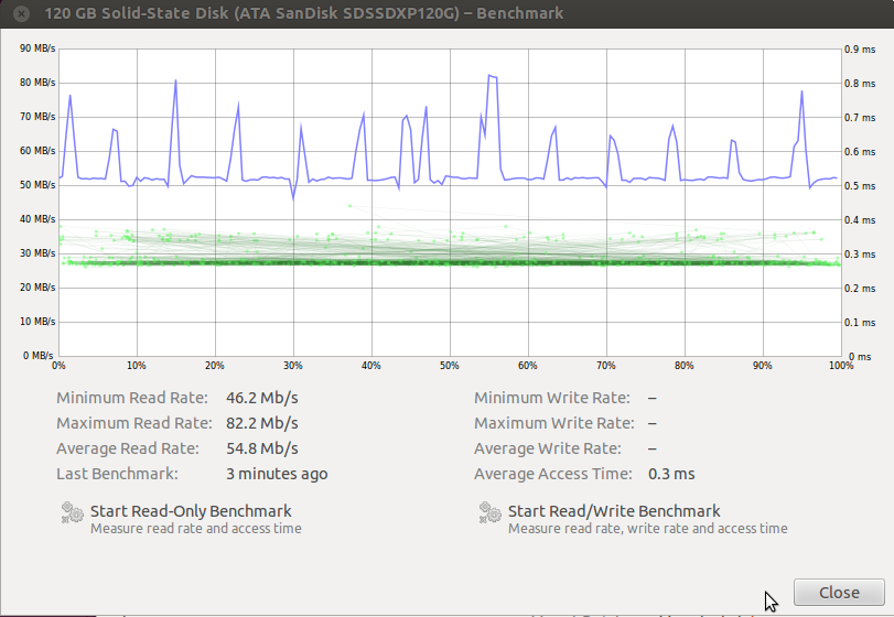
Note that there can be errors with eSATA / USB3.0 casings. I initially chose one which uses the Prolific PL2773, which implements the attachment as a USB Bulk-Only Mass Storage Class. Unfortunately this storage class doesn’t have the capability to pass TRIM commands.
But, although the attachment for the SSD doesn’t have TRIM capability, the SSD reports that it does have this capability, via eSATA, and this confuses the Kernel.
Errors are caused by the Kernel calling for TRIM on the swap space during the boot process.
How to fix this? Well the simplest way is to throw away the disk casing and connect the SSD drive directly. So, this is what I did. The disk performance also increases markedly too!
UDOO SSD speed testing
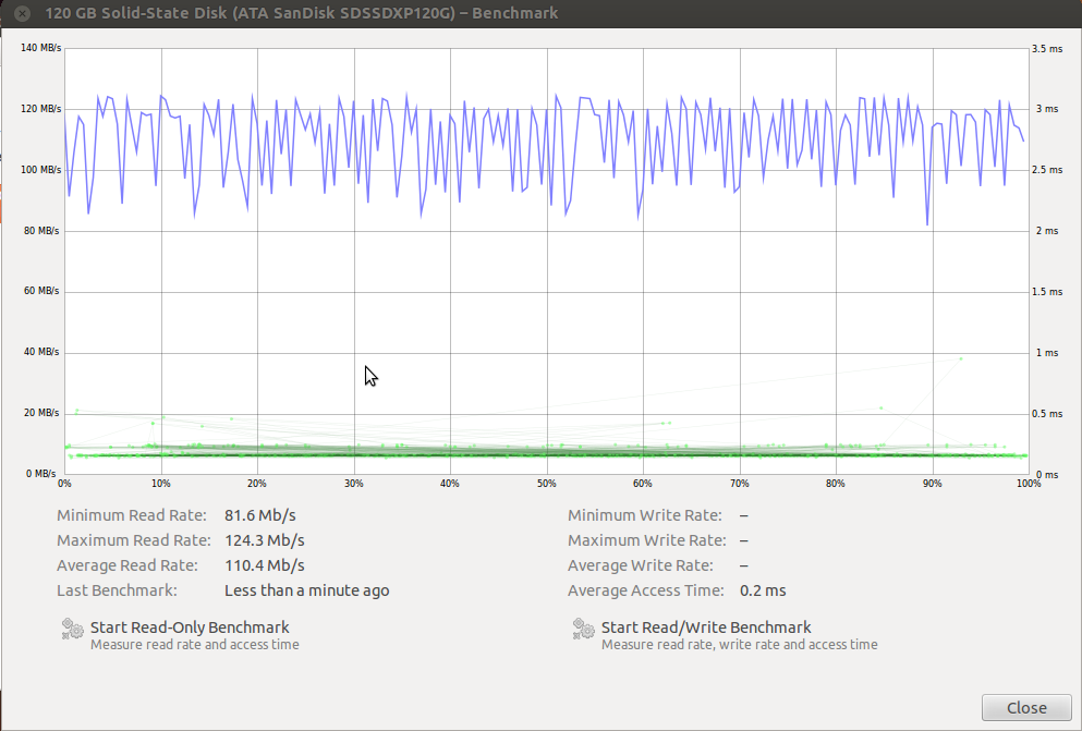
The UDOO SATA port doesn’t achieve quite the same throughput as the amd64 desktop does over USB3. But the speed increase over the uSD card is significant, and is very noticeable in use. Worth doing, in any case.
After removing the SSD drive from the housing, and driving it directly, the performance increase can be seen. The average read rate has doubled to over 110MB/s and the access time has decreased by a third making it about the same speed as on the amd64 desktop.
In practice the desktop feels even smoother. Great result!
Recently, my Quad core UDOO board arrived in the post. Initially, I tried the two provided uSD cards, with Ubuntu 11.10 and Android 4.2.2. I was a little disappointed that the Android version didn’t seem to work out of the box, but probably I did something wrong. What was more disappointing was that the provided Ubuntu operating system Ubuntu 11.10, is already past End of Life. Releasing a brand new device with an EOL operating system; I’m not sure what the UDOO team (or actually Freescale) are thinking.
Ok, so It is time to go my own way to get something that will remain viable for the long term. I use Ubuntu 12.04 LTS on my machines that aren’t running debian. So it is natural that I’d try the same Ubuntu Precise LTS solution, which is supported through to 2017, on my UDOO board too.
A bit of searching found Dave Cheney, who has written about installing Precise on his UDOO quad. However, Dave assumes that there is a working UDOO Linaro system from which to derive the result. I didn’t have that starting point, so I needed to find a solution from the uSD card inserted into my amd64 (Intel) machine, and build from a chroot armhf on amd64 solution. Fortunately, there are some references for how to take this path too.
Following this initial process, there are quite a few steps to get to a desktop GUI from the very simple Ubuntu core file system starting point, none of which are documented clearly. So, knowing that I’d need to take this path again (after I break something) it is time to write the steps down.
Get all the pieces of code necessary
From the UDOO Downloads page, get the latest versions of U-boot, Kernel, and Kernel Modules, relevant for your UDOO. Either the Quad versions or the Dual versions.
From the Ubuntu Core page, download the ubuntu-core-xx.xx.xx-core-armhf.tar.gz latest version that is there when you read this. At the time of writing it is 12.04.3. I’m led to believe that any recent version of Ubuntu Core would also work (see comments). There’s plenty of opportunity to experiment.
Prepare the uSD Card
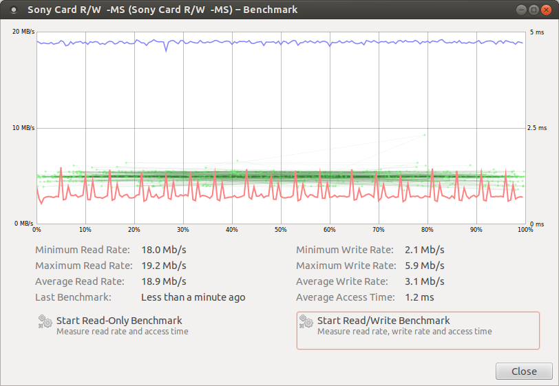
Use the largest uSD card that you can find. Also, get the fastest one available at a reasonable price. I have now loaded the system on to a Sandisk Ultra uSD card, and compared the speeds to a Sandisk “Black” card. It is worth getting a “faster” uSD Card for the operating system, but perhaps not especially the “fastest”. The Black card’s performance is quite variable, and particularly the Average Access time ranges from 1.4ms up to 3ms, whereas the Ultra card’s Average Access time is consistently 0.9ms to 1.0ms after repeated testing. The other parameters seem consistently similar.
Black (Class 4 ) Minimum 19.5Mb/s Maximum 22.4Mb/s Average 21.0Mb/s Access 1.5ms
Ultra (Class 10) Minimum 19.6Mb/s Maximum 22.5Mb/s Average 21.0Mb/s Access 0.9ms
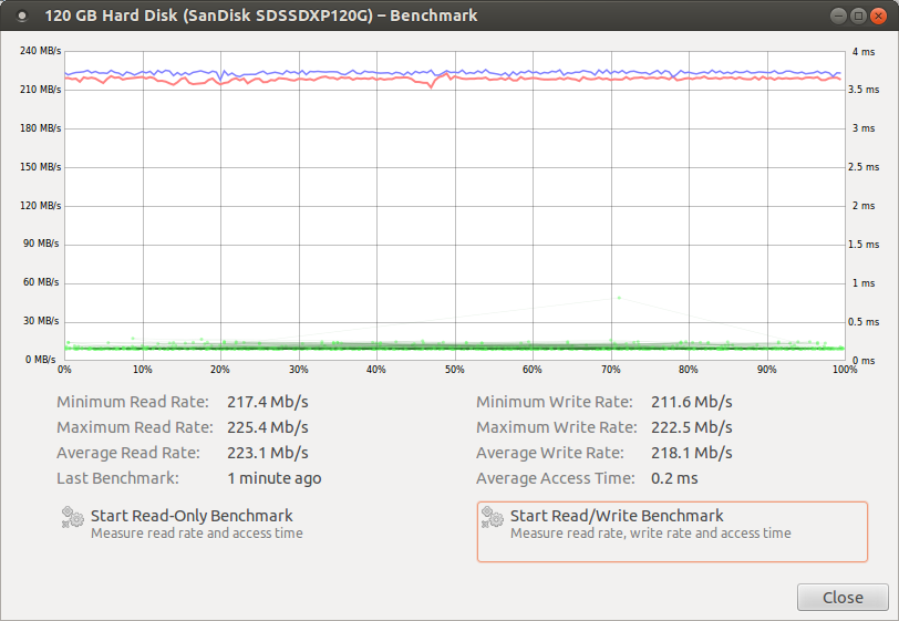
I have done some testing with a SATA SSD to compare it with these uSD Cards. If you can use a SSD as the root disk, then you’ll have a much more responsive experience.
Extreme ii SSD Minimum 81.6Mb/s Maximum 124.3Mb/s Average 110.4Mb/s Access 0.2ms
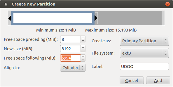
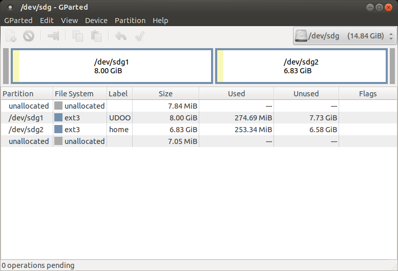
The elinux wiki has instructions for creating a bootable uSD card for UDOO. These are easy to follow, so I’ll not repeat all the details here. Using GParted I only left 8 MByte space before the start of the primary partition, and I labelled it “UDOO”. I also split the card in half, creating a secondary partition for the /home partition. This may take some time to complete, if your uSD is slow…
Before mounting the newly created filesystems, install the U-boot file into the first 8 MByte of the uSD card. Be sure to pick the descriptor for the root of the card (not the first partition). For me <MICROSD_DEVICE> is /dev/sdg.
Be very sure you’ re using the correct device; using the wrong device identifier will result in the loss of all data on the Hard Drive of the host PC used as you will overwrite the MBR.
Mount the just-created root partition on the uSD card. It will appear at /media/UDOO if you chose the same label as suggested. Then extract the tar.gz file containing the file system onto the uSD card with the following command, where <NAME_OF_TAR_FS> is the Ubuntu Core file downloaded previously.
sudo tar -xzvpf <NAME_OF_TAR_FS> -C /media/UDOO/
First, extract the Kernel Modules to the same current folder, and then copy the Kernel file and the Kernel Modules to the uSD.
So, now the uSD card is complete, and the new Precise UDOO should boot.
But wait,… there’s more. The Ubuntu Core is absolutely the minimum required to get started. There’s not even a user defined, so if we want to log into the new system we have to do a little more to get ourselves started.
Chroot from amd64 into armhf
To be able to execute armhf commands from an amd64 platform we need to use qemu. So for that to work we need to make sure we’ve got qemu installed on the host platform. Check using dpkg.
dpkg -l qemu-user-static
Have your SD Card mounted on your Linux PC and go to your Ubuntu Core folder:
cd /media/UDOO
Copy the qemu for arm file:
sudo cp /usr/bin/qemu-arm-static usr/bin/
Make sure you have your network settings properly configured:
The UDOO serial port (the uUSB connector closest to the corner of the board) operates at 115200 baud, but by default the Ubuntu Core image is not configured to take over on /dev/console at the correct baud. The simplest solution to fix this is to copy the tty1 configuration to the console configuration, and then adjust to the correct baud rate.
cp /etc/init/tty1.conf /etc/init/console.conf
vi /etc/init/console.conf
change the last line to
exec /sbin/getty -8 115200 console
Enabling the Ethernet
The wired Ethernet port is not automatically enabled. Edit the interfaces file and add two lines.
vi /etc/network/interfaces

auto eth0
iface eth0 inet dhcp
Other Niceties
Obtain the Ubuntu universe packages. The /etc/apt/sources.list file has most of the sources commented out. These comments should be removed, before installing a GUI.
vi /etc/apt/sources.list
Leaving the ‘chroot’
If you want to get out of the ‘chroot’ just type:
exit
Un-mount the target filesystem: Make sure you stay at the UDOO root point /media/UDOO/ and run the following commands. Go back to the original network settings. And the qemu can be removed too.
for m in `echo 'sys dev proc'`; do sudo umount ./$m; done
sudo mv etc/resolv.conf.saved etc/resolv.conf
sudo rm usr/bin/qemu-arm-static
sync; sync
Booting into UDOO Precise LTS
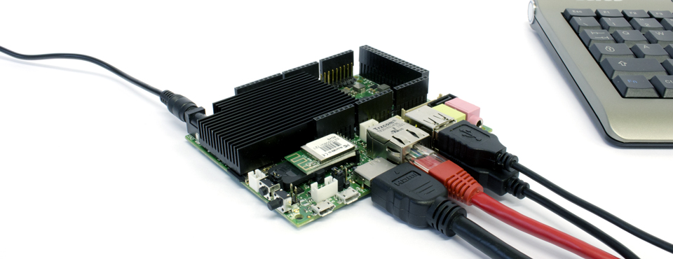
Insert the new UDOO Precise LTS file system uSD into the appropriate place, and then start up the serial console to watch the system boot. The serial port uUSB connector is the one closest to the RESET button, and should be connected at 115200 baud 8n1. It will appear on an amd64 Ubuntu machine as /dev/ttyUSB0.
When the system is booted the hdmi interfaced terminal should work successfully too. Use the login details you created above to log in, and profit!
Building the Desktop
From this point it is possible to install the GUI of choice. I have tried with LXDE, but given this is a Quad Core device, it may well run well with the standard Unity Desktop.
Installing LXDE or Unity (the standard Ubuntu desktop) can be done once you’re logged into the UDOO board, by either of these commands.
sudo apt-get install lxde-desktop
# OR
sudo apt-get install ubuntu-desktop
Once you have rebooted into your new desktop, it is useful to move the home directories over to the second partition that was prepared. The full desktop environments identify the second uSD partition and mount it automatically as /media/home.
sudo cp -rp /home/* /media/home
Edit the /etc/fstab file to get the partition to mount at /home, and reboot.
One thing missing (in a short amount of testing) is the firmware for the WiFi device. The best place to find the latest firmware-ralink is in the debian Sid repository. It is the same file for all architectures.
sudo dpkg -i firmware-ralink_0.43_all.deb
Final Thoughts
Compared to the Raspberry Pi the UDOO environment certainly runs very hot. The large heat sink on the UDOO is very necessary, whereby the Raspberry Pi doesn’t even need a heatsink. I guess that Freescale has packed a lot more (4x more?) into the same space that Broadcom used for its design, and that consumes more energy. Certainly, the lack of a GPU driver module and user space tools for the display, forcing software rendering doesn’t help. Hopefully Freescale will get their act together soon and Open Source the Vivante GC2000 driver code, or at least the hardware definitions to allow the Etnaviv team to progress quickly.
Neither Raspberry Pi nor UDOO are capable of being battery powered devices, which makes them pretty useless for any Internet of Things sensor project, IHMO. So, I’m not sure what kind of applications they’re really trying to address? Doesn’t matter, they’re still pretty cool devices and I’m going to be using the UDOO often.
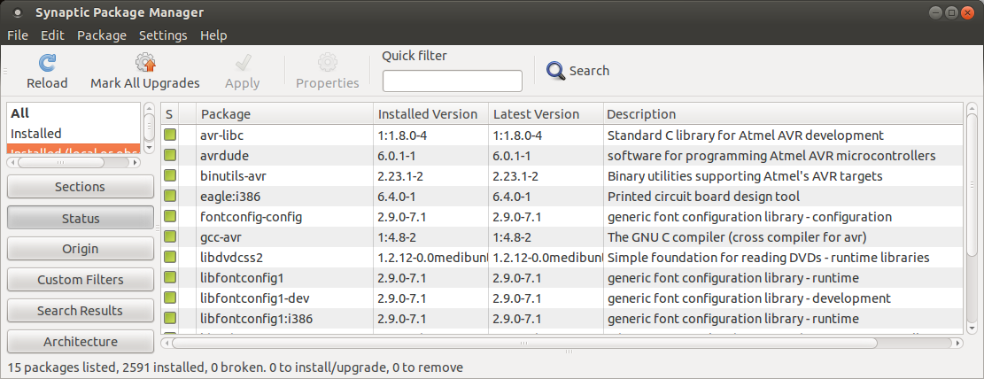
Always looking for the latest and greatest code for AVR, I scan the debian Sid repositories every few months for updated packages to use. Recently debian Sid included the latest gcc-avr 4.8 package, binutils-avr and the new avrdude 6.0.1 package. So I had to install them all to test.
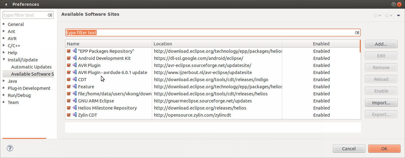
Unfortunately, there is a new device format used in the avrdude.conf file which breaks the standard Eclipse AVR Plugin, rendering the MCU choice ineffective.
Asking a question on avrfreaks.net found the answer. keestux has fixed the problem and has released an interim AVR Plugin 2.4.1 which incorporates a fix for the change in avrdude.conf file format.
I guess it is no secret, the reason why I’ve put so much effort into getting the Goldilocks 1284p board built. I was looking for a platform that would allow me to experiment with the uIP TCP/IP and UDP/IP stack with the most performance and flexibility possible while still being compatible with the huge range of sensors and actuator Shields that form the Arduino legacy. From the microprocessor view, the ATmega1284p used in the Goldilocks certainly achieves that goal.
I’ve written in a previous post about the theoretical performance difference between the common Wiznet (or IINChip) W5100 used in almost all Arduino Ethernet shields and the component I have selected that uses the W5200 to provide the Ethernet interface. This post demonstrates the real world performance differential with a simple example.
But first, I am happy with the result of the uIP port to the Wiznet platform within freeRTOS. I’ve taken some of the old uIP v0.9 and v1.0 files from many sources, and updated them with the latest snapshot status from Contiki 2.7, to try to bring the last 5 years of experience into the result. Whilst the resulting codebase has not as yet been extensively tested, it seems to work as expected.
Results
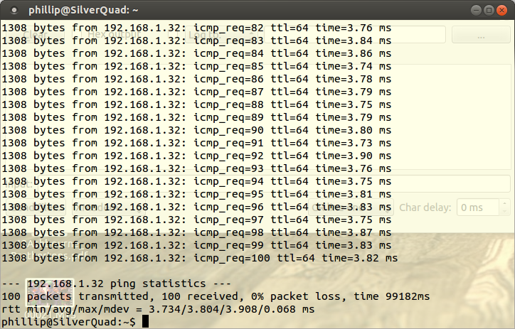
This is a simple test, sending 1300 byte PING packets to the MACRAW interface on the IINChip to be handled by uIP. After 100 PINGs the W5200 takes on average 3.804 ms, whilst the W5100 takes on average 22.109 ms for each round trip.
This means the W5200 is nearly 6x faster than the W5100 in real world performance.
Of note, this real world result is achieved whilst over-clocking the W5100 SPI bus out of specification at 5.5MHz (being SCK/4), rather than at 4MHz which is the specification. The W5200 SPI bus can, of course, run up to 30MHz or faster, so its limits are not even being tested by the Goldilocks ATmega1284p MCU.
W5200 SPI bus
The key differential which provides the W5200 its performance advantage is the use of multi-byte burst transfer mode for moving payload data into and out-of its controlling MCU. In theory the entire 32 kByte Address space of the W5200 could be transferred in one transaction. In practice, a full Ethernet frame can be transferred in just over 1 ms.
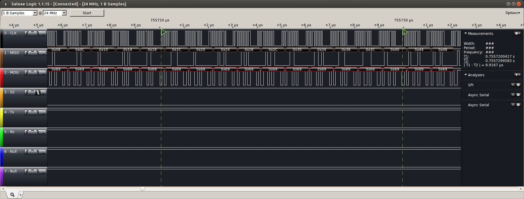
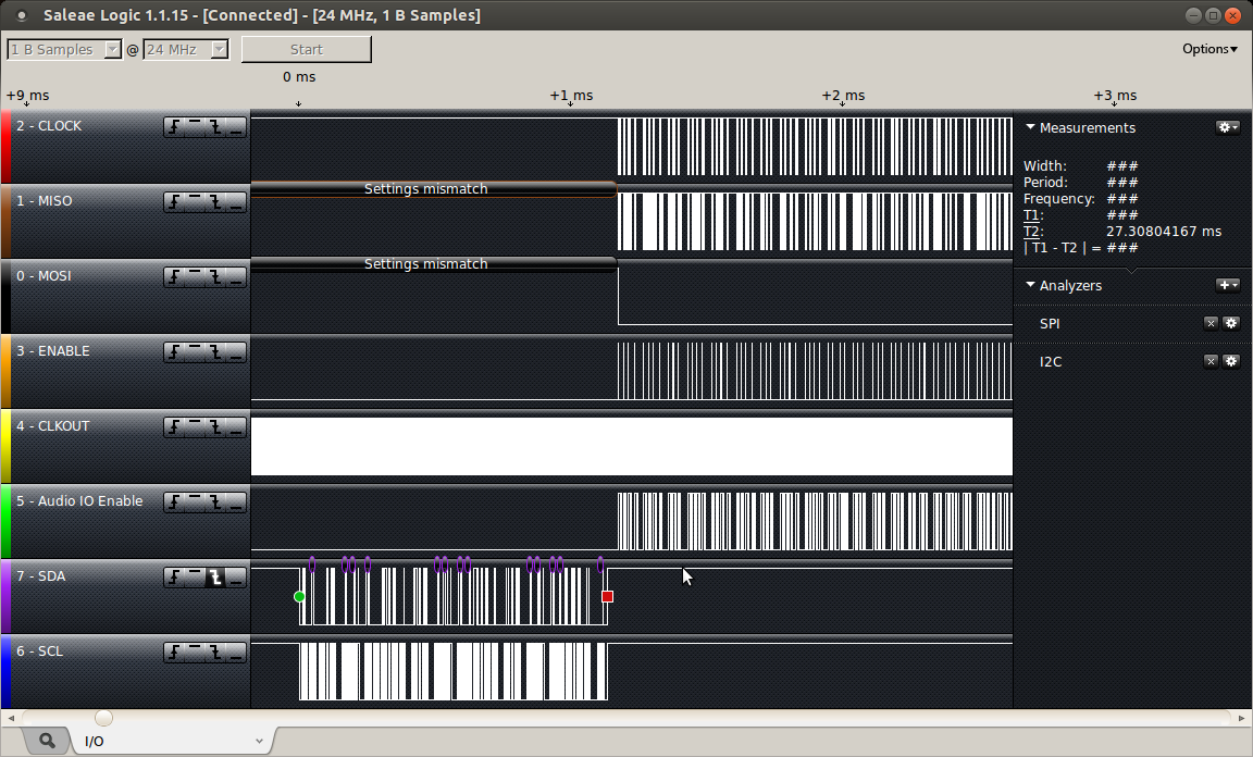
These shots show how the W5200 SPI multi-byte transfer works in practice.
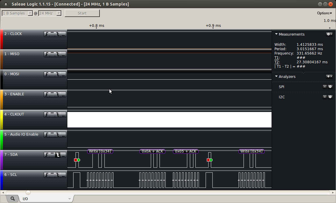
The W5200 supports multi-byte burst mode transfers on the SPI bus. This is a 1300 Byte PING frame transfer out of the W5200, and returned by the AVR.
This screenshot shows an entire received 1300 Byte payload PING frame being transferred in 1.34ms.
The AVRmega1284p generates a PING response frame, and transfers it back to the W5200 in one burst mode transfer.
The Goldilocks AVR1284p takes 0.29ms to generate the response PING, and then it is transferred back to the W5200 for transmitting on the wire.
Detail of the burst mode multi-byte SPI transfer capability of the W5200.
This screenshot shows the detail of the transmission of the PING frame to the AVRmega1284p. Note that each Byte takes less than 1 us to transfer.
W5100 SPI bus
The W5100 SPI bus uses a 4 byte transaction to transfer a single payload byte, and it is not capable of a multi-byte burst mode.
The Wiznet 5100 uses a 4 byte protocol to transfer a single data payload byte.
This screenshot shows the detail of the transmission between the AVRmega1284p and the W5100. It shows that to transfer 1 payload byte it takes about 0.036 ms (which is 36 us or 36x longer than the equivalent transfer on the W5200).
Conclusion
If you’re planning on building anything that relies on wired Ethernet, then go out of your way to find a Elecrow W5200 Shield or Seeed W5200 Shield. It is about six times faster than the common W5100 in the real world testing, and has many other great features.
uIP works well on the Goldilocks and provides a great platform for developing TCP/IP and UDP/IP stack applications.
Next steps are to implement CoAP and MQTT clients on this platform, to increase my understanding of both of these important IoT protocols.
For a long time the standard Arduino Ethernet Shield has been driven by the Wiznet W5100 Internet Processor. This shield and the chip upon which it is based forms the basis of just about every IP enabled networking project in the Arduino world.
The Wiznet W5100 chip has some interesting features, such as direct and indirect memory access, but it has some severe limitations in its SPI bus capabilities . Also, the W5100 can support only 4 ports within its hardware IPv4 engine. Unlimited software ports can be added, by providing your own IP stack in MACRAW mode using Port 0, but that is not the road well travelled.
There are two major issues with interfacing with the W5100. First, the SPI interface is only specified to run at 4MHz. And second, the SPI interface supports only a byte mode transmission.
The limitation in SPI rate to 4MHz means that the standard 16MHz Arduino board SPI bus cannot be driven at any speed greater than SCK/4, if it is to remain within specification for driving the W5100. 20MHz boards, such as the Goldilocks, it must drop to SCK/8 if they are to remain within specification.
Also, the W5100 byte mode transmission requires a 4 byte SPI bus transaction for each byte of data to be transferred into and out of the network interface.
Counting the (unachievable) theoretical best case rate for the W5100, it means that 4 * 8 * 4 = 128 system clocks elapse to transfer a single byte of data. Ugh! Slow.
What to do?
I guess Wiznet must have realised this performance issue (which is more apparent with more capable 32 bit MCUs which run at higher system clocks than the slow old 8 bit AVR ATmega range) and they’ve recently released the W5200 as a replacement (specific to SPI bus interfacing) for the W5100 chip.
Wiznet 5200
The W5200 brings a number of new performance features to the game, based on the well known and understood IPv4 network engine of the W5100. The table below contrasts the two chips.
Key features comparison W5200 vs W5100
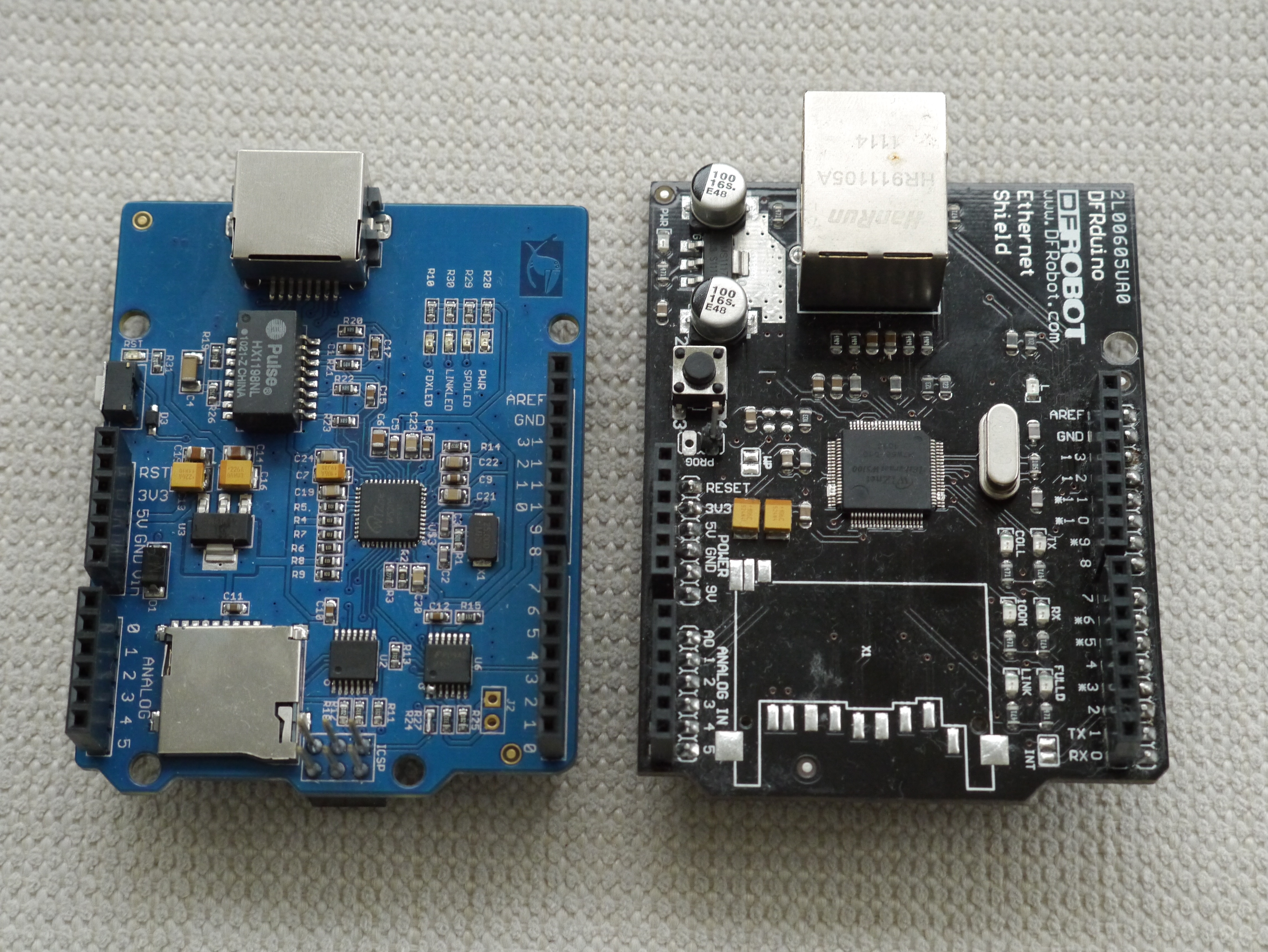
The W5200 is a much smaller and simpler chip to locate on the board, and it is easier to solder for those interested in private SMD constructions. Importantly for networking performance, the W5200 has twice as much Tx/Rx buffer memory for IP packets, and supports 8 simultaneous hardware IP sockets. These features make the W5200 a great performance increment on the W5100, and already sufficient to make a switch. An example of the size of the two chips compared can be found below, with the Elecrow W5200 on the left and an old DF Robot W5100 v1.0 on the right.
Elecrow W5200 and DF Robot W5100 v1
However, the greatest improvement in the W5200 lies in the area of the SPI bus interface. Wiznet has ditched the Direct addressing mechanisms (that took all the pins) on the W5100, and made the W5200 a SPI specialist, capable of running at up to 80MHz clock. That is a 20x increment.
Additionally, the W5200 supports SPI burst mode transmission. This means that up to the full Tx/Rx buffer (32kByte) could be read or written written in one transaction.
In the Arduino situation the W5200 can be driven at SCK/2, the maximum SPI speed achievable on an AVR ATmega MCU, and each byte takes one SPI byte to transfer. This means we can achieve a rate of 2 * 8 * 1 = 16 system clocks to transfer a byte of data.
This means the W5200 is 8x faster for the Arduino, and for Goldilocks 20MHz boards it will be 16x faster than the W5100 – fast as a leopard!
A practical analysis of the speed difference between the two Wiznet chips is here.
Easy to use.
The W5200 is easy to use, and easy to get.
Wiznet have provided some ready made W5200 driver files to include into the Arduino IDE. These replacement drivers for the existing W5100 driver files provided within the IDE just have to be substituted (or overwritten) to enable the slightly different SPI interfacing requirements of the W5200. They also provide C code drivers, which I used as a basis for my AVR freeRTOS code.
The Socket API provided by the W5100, and utilised by the Arduino IDE remains unchanged in the W5200. This means that it is only the performance enhanced SPI bus interface that needs to be rewritten to take advantage of the burst mode transmission, and the slightly different register locations associated with the increased Tx/Rx buffer and number of sockets available.
W5200 functional blocks
I was waiting for a long time for the W5200 to be put onto an Arduino compatible shield, so that I could use it easily. Suddenly, there are two on the market. One from W5200 Shield from Elecrow in China, and the other W5200 Shield from Wiznet.
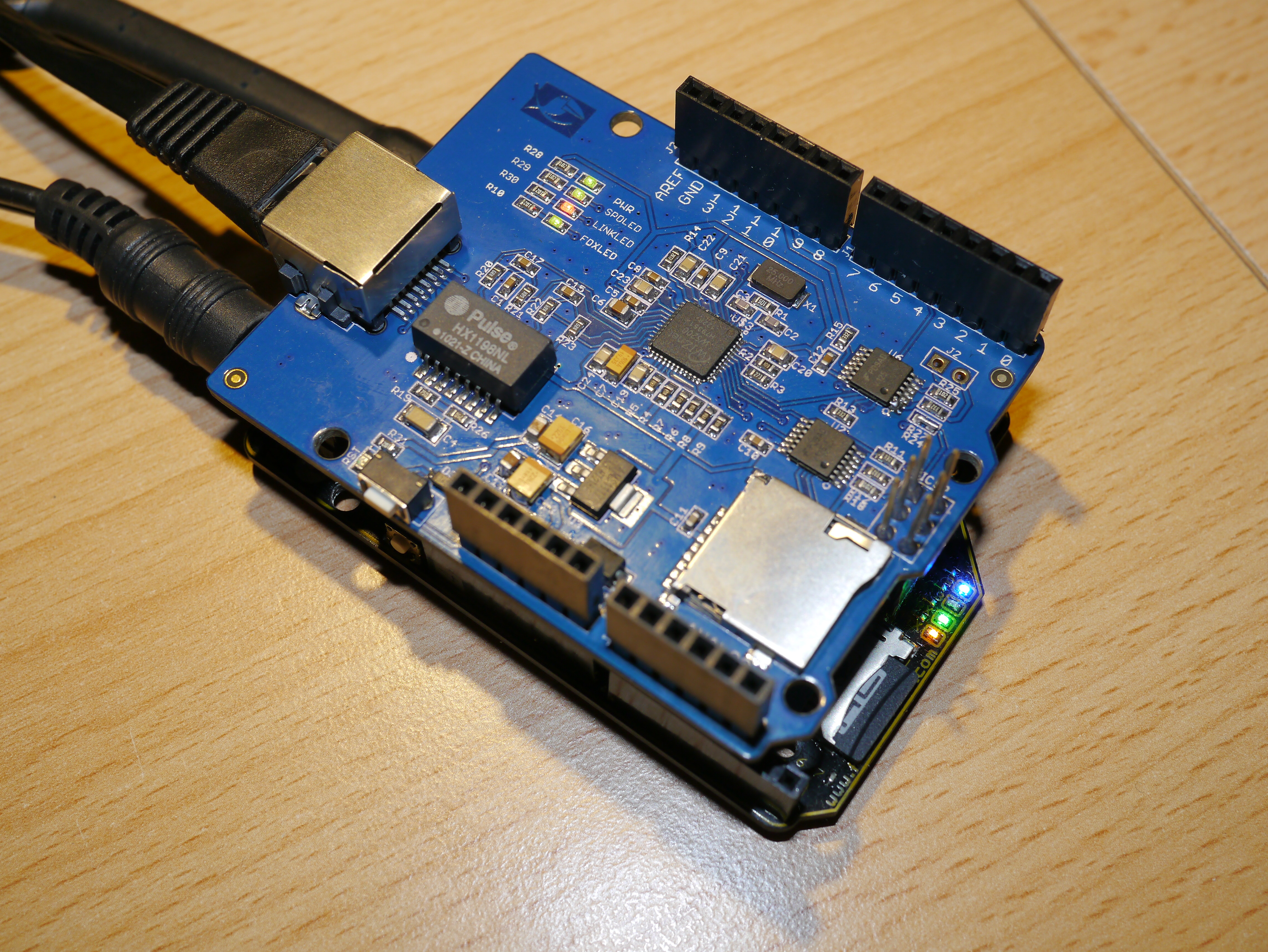
I decided to purchase some of the Elecrow W5200 Shields. They looked to have a much better design than the Wiznet version, because Elecrow have utilised proper 5V to 3.3V buffers to ensure the safety of the on board uSD card, and have designed using the Arduino R3 standard.
The key and unique (afaik) feature of the Elecrow W5200 boards is the use of the lowered RJ45 jack, that allows the Ethernet shield to between other boards with no clearance problems. I have taken some pictures to show the difference between the standard RJ45 jack and the Elecrow W5200 board version, mounted on a Goldilocks board, and a standard Arduino Uno, with a LCD Touch Shield (even with under-slung SD Card cage) mounted over the top.
Some small improvements.
I spent some time working with the Elecrow W5200, and have been in discussion with Richard and David (Tech Support) at Elecrow about the implementation. They have been very helpful in resolving some issues I have found in using their design.
Firstly, they have used quite a high resistance on the PWDN pin (which is intended to allow the W5200 to be powered down to reduce energy consumption). There is insufficient current on this resistor to hold ground, and sometimes the W5200 slips into PWDN mode and can’t be addressed. This can be solved by pulling jumper J2-2 to ground, or (permanently) by bridging Pin 1 and Pin 2 on U6 which is the buffer chip controlling the PWDN line. Check the schematics to see why this is so.
Secondly, the buffer chips used are driven from from 3.3V for Vcc. They are a little slow (100ns/V skew) at this supply voltage, and for the return data path on the MISO line they should properly be driven from 5V Vcc. At 5V Vcc the buffer chips are also much faster (20ns/V skew). The slower buffer chips, the LPF characteristic generated by the sensibly included output resistors, and the lower logic level compared to the AVR 5V TTL levels all combine to reduce the speed at which the SPI bus can work. Whilst the correct resolution is to drive the buffer chip at 5V Vcc for the inbound (AVR point of view) signal lines, I have found it is sufficient to remove and bridge the R24 resistor to achieve the SCK/2 SPI rate we desire.
This view of the Elecrow W5200 board shows the modifications in detail. I believe that later versions of the board will resolve these issues. And, with the Elecrow W5200 Shield’s unique recessed RF45 connector’s advantages and the speed of the W5200 MCU, all other sins are forgiven.
Elecrow W5200 showing R24 delete and U6 Pin 1-2 bridge.
TL;DR
The Elecrow W5200 is a very speedy and easy to use alternative to the standard Arduino W5100 based solution. It is a great addition to my collection of IPv4 networking shields.
A practical analysis of the speed difference between the two Wiznet chips is here.
There’s a great new Arduino Uno (pre-R3) Shield available from Open Music Labs. Their Audio Codec Shield is an Arduino shield that uses the Wolfson WM8731 codec. It is capable of sampling and reproducing audio up to 88kHz, 24bit stereo, but for use with the Arduino it is practically limited to 44kHz, 16bit stereo. The Audio Codec Shield has 1/8″ stereo input and headphone output jacks, a single pole analogue input aliasing filter, and 2 potentiometer for varying parameters in the program on the fly.
The Open Music Labs provides a some libraries and code examples for use with the Arduino IDE, and also with the Maple IDE. But, rather than just use the existing code, I thought it would be fun to develop some freeRTOS libraries from their basis code.
I spent quite some time understanding exactly how the WM8731 worked, and what was needed to make it perform, in a RTOS environment. It is clear, that to work at the audio rate of 44.1kHz, that the Arduino needs to be clocked by a hard interrupt, rather than by a soft timer. So, I spent some time designing and playing with different methods of driving the board.
Initially, I thought it would be good to limit the interrupt processing to constant clock in and clock out of data, that MUST happen every sample (at 44.1kHz) or the sound sampling or playback is simply broken, and allow the interrupt to semaphore a further processing task to wake it up. However, once I understood just how limited the time available is for processing, it became apparent that (at least for the 16MHz Arduino) there is no time left to muck about with a RTOS, and everything has to be kept as simple and regular as possible.
Never the less, the freeRTOS code is useful to provide serial and I2C libraries to set up the board, and possibly to do some other tasks where possible.
The resulting code consists of just one freeRTOS Task, that initialises the Shield, and then suspends itself indefinitely. The freeRTOS Scheduler keeps on running, but finding no available task will just pend itself until its next timer tick.
  AudioCodec_ADC_init();    // initialise the potentiometer sampling.
  AudioCodec_SPI_init();    // initialise the SPI bus for special purpose Audio Codec use.
  AudioCodec_init();        // initialise the Audio Codec using I2C bus.
  AudioCodec_Timer1_init(); // set up the sampling Timer1, runs at audio sampling rate.
  vTaskSuspend(NULL);       // well, we're pretty much done here...
First the Arduino ADC is initialised into free running mode, to provide inputs from the two potentiometers on the Shield. The Open Music Labs have provided an analysis of the Arduino ADC, and they show that the free running mode provides the lowest noise floor. Not that it is important to have a low noise floor for this purpose, as it is just potentiometer sampling. However, they missed the trick of using decimation to improve the sampling resolution, choosing instead to use a dead-band for the sampling. I’ve changed the ADC initialisation to do variable sample decimation, depending on the bit depth desired.
This is the example code for a single potentiometer.
static inline void AudioCodec_ADC(uint16_t* _mod0value)
{
  if (ADCSRA & (1 << ADIF))     // check if sample ready
  {
    _mod0temp += ADCW;  // fetch ADCL first to freeze sample is done by the compiler
    ADCSRA = 0xf7;      // reset the interrupt flag
    if (--_i == 0)      // check if enough samples have been collected
    {
      _mod0temp >>= DECIMATE;   // Decimate the summed samples
                                // (to get better accuracy), see AVR8003.doc
      *_mod0value = _mod0temp;  // move temp value to the output
      _mod0temp = 0x0000;       // reset temp value
      _i = _BV(2 * DECIMATE);   // reset loop counter
    }
  }
}
Then the SPI bus is configured to sample the data from the ADC on the WM8731, and to write data back to the DAC. Since we’re using the DSP interface, which is very similar to the SPI bus interface, with 16 bit transfers, the SPI mechanics can be used effectively, removing the need to bit-bang the interface. I found that although SPI Mode 0 nominally looks to be correct, it would lose the most significant bit of most transactions, being the left channel input values. I needed to use Mode 3 to get effective transactions.
The I2C bus is used on pins A4 and A5, which is pre-R3 format. I would digress to say that decision not to continue to support the SDA/SCL pins being available on A4 and A5 is a very bad one, in my opinion. There are many old, and this quite new, Shields that will simply be broken by this decision. Simply, bad for the Arduino legacy.
I have completed the register and pin definitions in the header file, to allow simple selection of the configuration, by adding the appropriate bit values into the register settings.
The initial I2C command transaction looks like this.
Here is a bit more detail on the DIGITAL_PATH_CONTROL command.
The true heart of the project lies within the use of Timer 1 to signal the 44.1kHz timing required to produce the sound samples. An interrupt driven by the Timer 1 counter signals the transfer of data, performing any audio processing required on the incoming data, and writing it to the output ready for the next transfer, and sampling the analogue potentiometers to use them as as mod inputs on the signal. The Timer 1 counter is incremented by counting the CLKOUT line coming from the Shield.
ISR(TIMER1_COMPA_vect)
{
  // WM8731 data transfer routine
  // move data from and to the WM8731 - done first for regularity (reduced jitter).
  AudioCodec_data(&left_in, &right_in, left_out, right_out);

  // audio processing routine - do processing on input - prepare output
  AudioCodec_dsp();

  // adc sampling routine
  // sampling the potentiometers (no sound here)
  AudioCodec_ADC(&mod0_value, &mod1_value);

  // end mark - check for end of interrupt - for debugging only
  PORTD |= _BV(PORTD6);   // Ping Audio Shield buffer line.
  PORTD &= ~_BV(PORTD6);
}
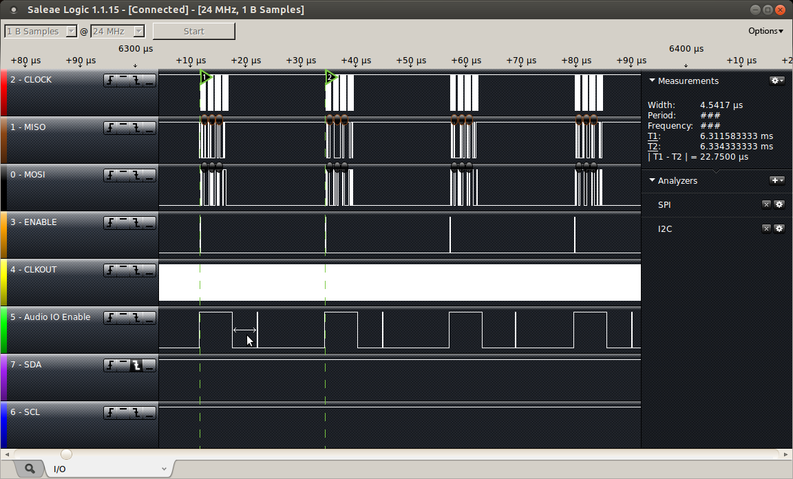
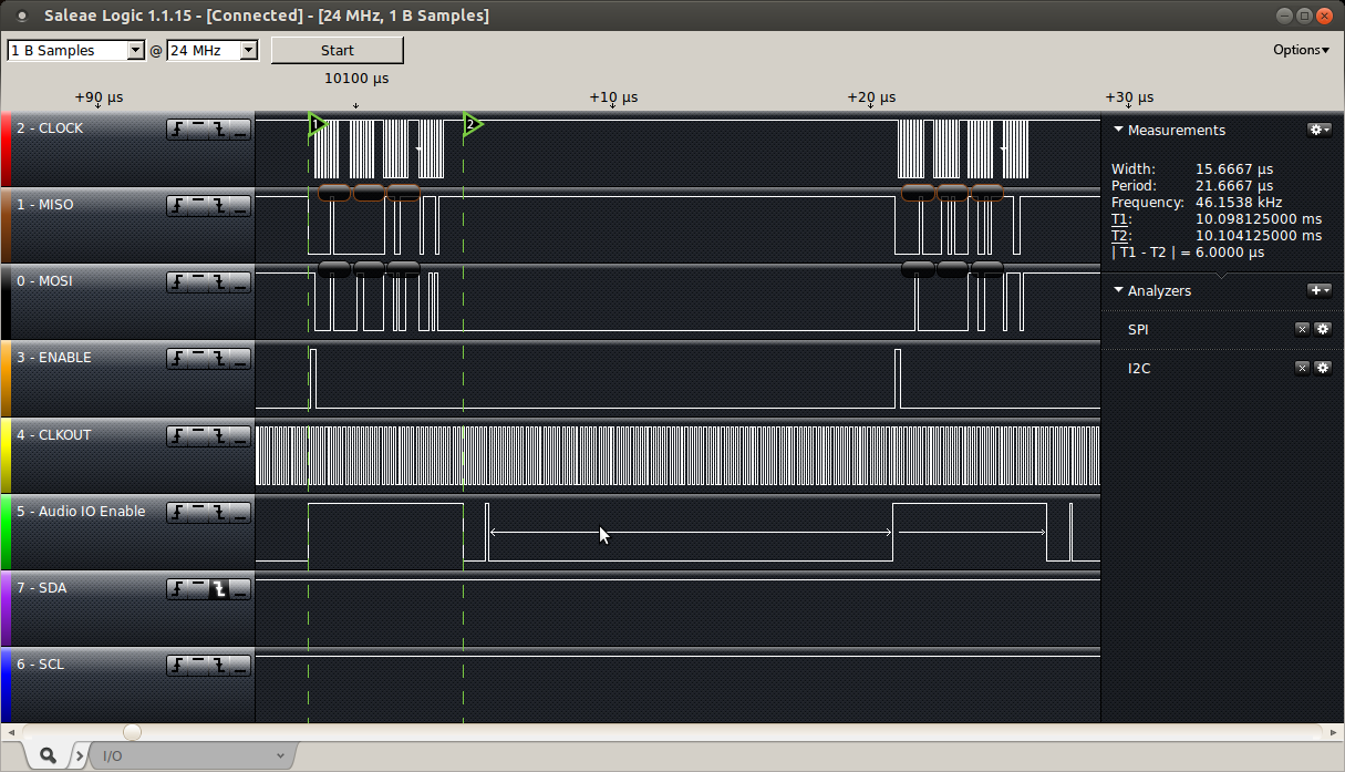
As I noted above, timing is everything. Based on the plots below, it takes exactly 6us for the AudioCodec_data() function to transfer the data from and to the WM8731. This doesn’t seem like very long, but to maintain a sample rate of 44.1kHz, each transaction must be completed in less than 22.7us, as shown below.
The logic trace below shows the situation with the simplest AudioCodec_dsp() function available. Here the DSP processing is completed with over 15.7us to spare. The actual AudioCodec_data() function takes exactly 6us to complete (T1-T2), and can be used as a scale for other logic traces below.
inline void AudioCodec_dsp(void) // straight through connection I-O
{
  left_out  =  left_in; // put in to out on left channel
  right_out =  right_in; // put in to out on right channel
}
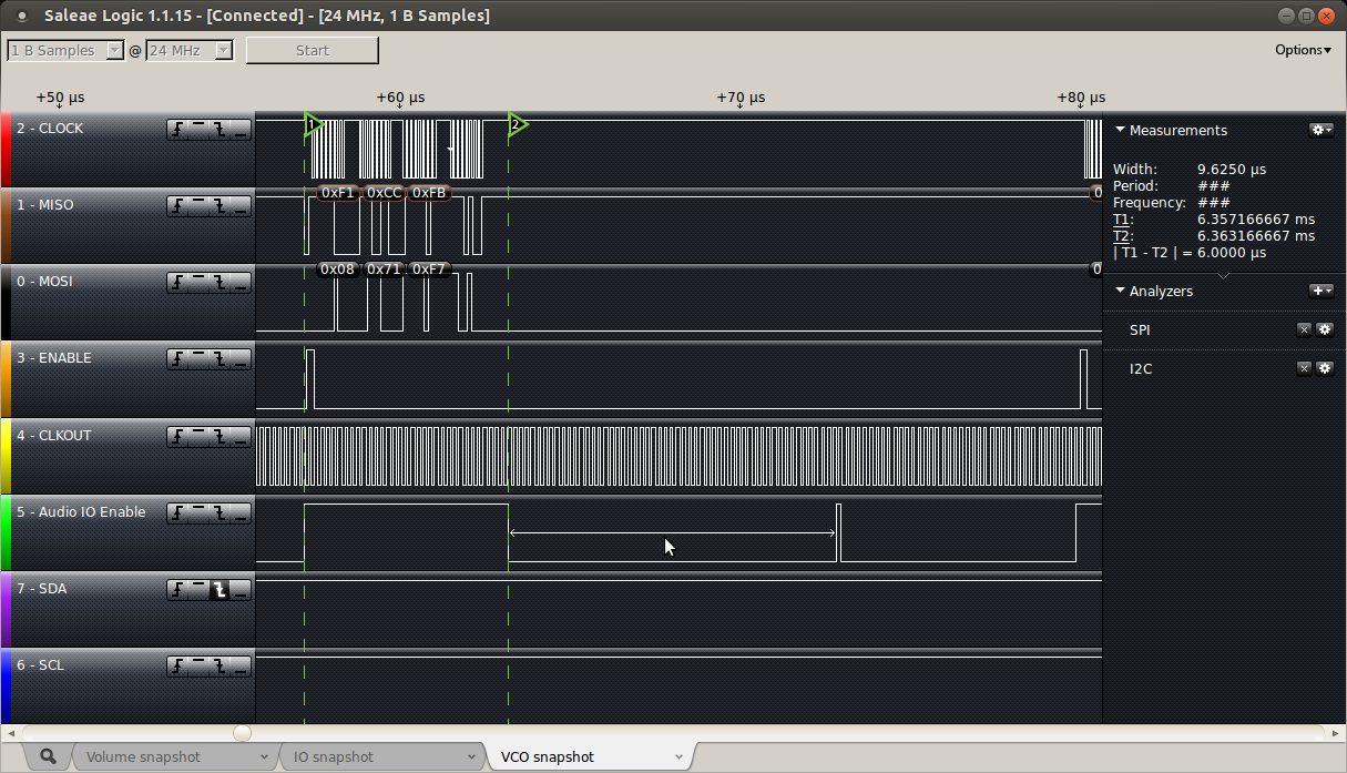
Other more complicated routines, such as a sine-wave Voltage Controlled Oscillator (digital of course) take a little more time from our limited budget, needing 9.6us to complete.
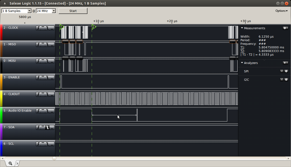
I have used the same code on a Freetronics Eleven, an Arduino Uno clone, overclocked to 22.1184MHz, and as can be seen below, it results in the AudioCodec_data() function taking 4.33us (vs 6us standard) and the VCO code taking 6.125us (vs 9.6us standard). Whilst these savings are relatively small, by comparing the two logic traces, I think they do change the result enough to make it worthwhile for this application.
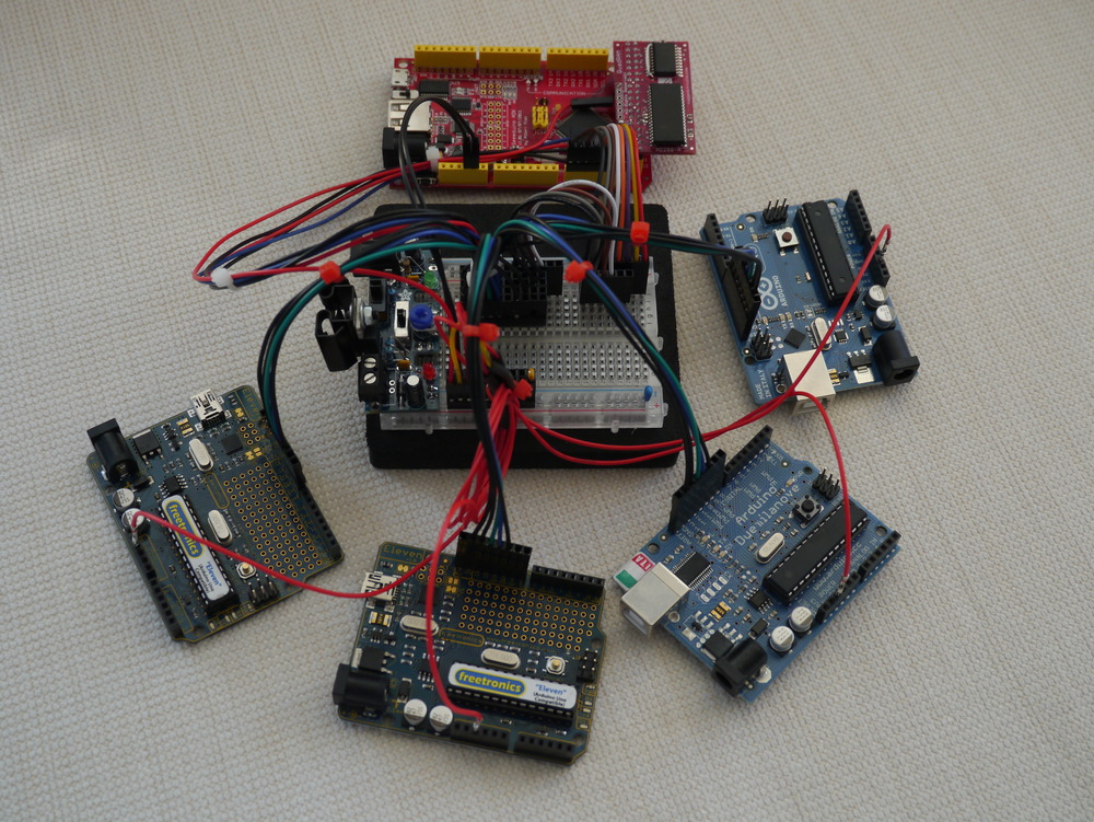
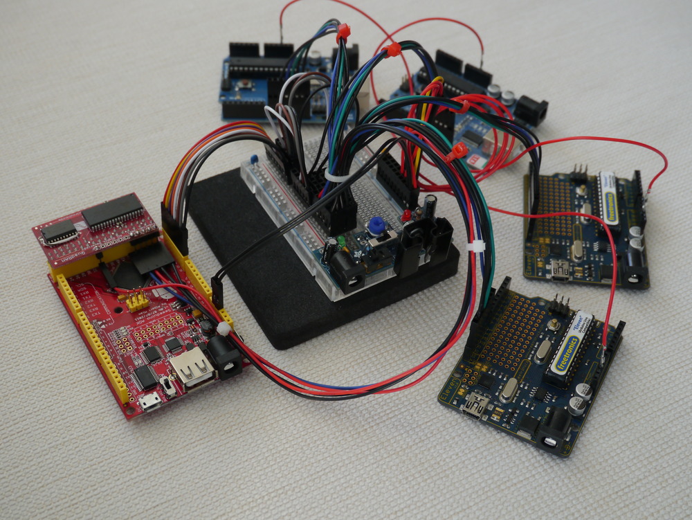
Since my last post on the ArduSat and the idea I had to use the Supervisor node, an ATmega2561, as the core of a centralised eXtended RAM system for the Client nodes, ATmega328p “Arduino” devices, I’ve been thinking and working on a solution for building a centralised non-volatile SD Card based storage solution.
With design, sometimes it is necessary to let an idea stew for a while before the right answer just sort of distils out of the soup. For the solution for this problem, this was the case. There was some thinking space required…
The Question
There are 16 Client nodes in the ArduSat platform. Each and any of them may wish to use the central SD Card to store information at the same, or at different times. How would it be possible to allow more than 16 files to be open on the one SD Card (connected to the Supervisor node) whilst maintaining consistency in the file system? How would access to the file system be scheduled?
The Tools
I have been using the ChaN FatFs file system libraries now for some time. They are fully featured and have a very clean design, fully separating the file system layer from the underlying physical media access layer (the drivers). This means that the file system tools can be implemented on many different architectures, with only changes to the driver layer (DiskIO) needed for each platform.
The Thought Process
My initial thought was that the Supervisor node should maintain the file system, and that I should write packaging for the FatFs file system commands to allow them to be remotely implemented across the SPI bus, in a similar manner as described in the XRAMFS post.
The idea of writing these “remote controls” for the file system commands was scary, as I recognised that there are 33 commands in the interface, and each of them has their own characteristics. Also, maintaining these interfaces would likely be problematic, as I would have to test each command extensively to ensure that there were no “thick thumb” errors introduced into the stable and proven FatFs library.
Some weeks passed…
Then at about 3am, I realised that the right answer was to write a “shim” between the standard FatF file system commands and the standard physical media drivers, and to have this shim operate across the SPI bus in exactly the same manner as the XRAMFS solution.
So, I wrote it.
The Solution
The solution separates the ChaN libraries into two parts. The file system part is resident on the Client node. Each Client node maintains its own view of the file system on the Supervisor SD Card. As the ChaN FatFs library is written for low memory devices, the file directory tree is refreshed each time a change in the working file is done. The Supervisor node only does the DiskIO under the command of each of the Clients.
There are only 5 relevant driver layer DiskIO commands. These commands are used in the Supervisor node to execute requests sent over the SPI bus from the individual Clients. Since there are only a small number of commands, and they are static and dependent on the architecture of the machine they’re running on, their functionality is quite constant. The Supervisor has no knowledge of the file system at all. It simply implements DiskIO commands on sectors of the SD Card as requested, one a time, as requested by Clients.
The Supervisor implementation simply expands on the existing Task loop established for the XRAMFS system, by adding in the 5 additional DiskIO commands. The added complexity, that the SD Card is accessed over the SAME SPI bus as the communications between Client and Supervisor, means that I had to introduce an interim “Pending” state for commands to allow the Client to wait for confirmation that a task has been completed or, in the case of disk_read or disk_ioctl, to recover the waiting data from the Supervisor.
The Client implementation inserts different shim DiskIO commands for the FatF system to call. These commands use the SPI bus to call the Supervisor, and enter a request. Some commands return immediately, allowing the Supervisor to continue with the command, once the command and any required data has been transferred. Other commands wait until they can retrieve information from the Supervisor, before returning to the FatF file system layer of the library.
In this solution, the XRAMFS was instrumental in simplifying the transfer of information. The exclusive availability of 16kB of RAM for each Client meant that disk_write or disk_read commands could cache their data in XRAMFS whilst it was actually written to or read from the SDCard. Because the RAM is available exclusively, there is no consideration that another Client may overwrite the results of a command, or that memory exhaustion may corrupt data.
When a Client program calls one of the FatFs library commands, it in turn calls one of the special ArduSat SPI DiskIO shim routines. These routines signal the Supervisor in the normal manner, and transfer any data associated with the command into the Page of XRAMFS assigned to the Client.
The Supervisor will then undertake the standard DiskIO command, retaining the result of the command and any data resulting from the command in XRAMFS.
Both Client DiskIO routines, and the Task running in the Supervisor are aware of the “Pending” state, which is where a DiskIO command has been completed on the Supervisor and there is data waiting in the XRAMFS for the Client to recover.
Once the Client DiskIO command completes, it returns the normal interface information to the calling FatFs command.
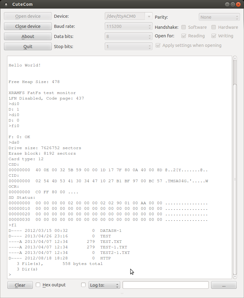
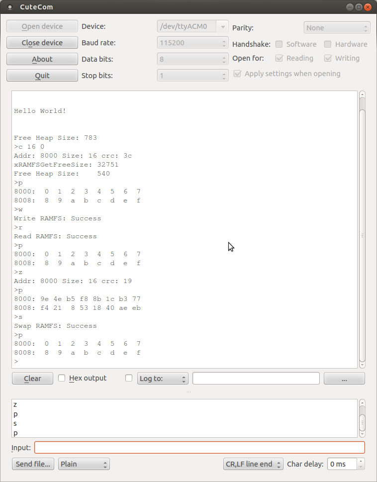
Here a monitor program on a Client is initialising the SD Card. If the Supervisor notices that the SD Card is not initialised, it will return Error, and then undertake to initialise the card. The second call for initialisation will then be successful. This decoupling method ensures that Clients cannot reinitialise the card, whilst other Clients may be using the Card.
The file system (on the Client) is then initialised Then, the SD Card status is read. Finally, the current working directory is read and printed.
In this screenshot, a file is opened for reading, and the file pointer set to the start of the file. A dump of the first 64 Bytes of the file is read and printed. Then the file is closed.
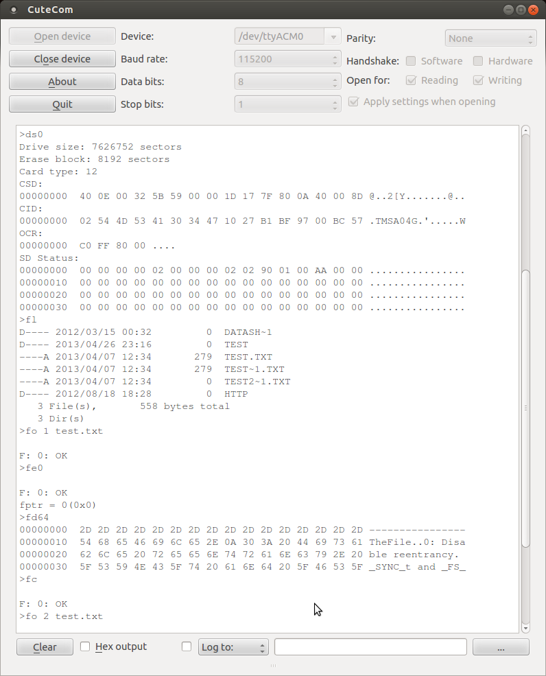
Here, the same file as above is opened for writing, and 45 bytes of 0x10 (16) are being written. The result is checked by opening the file for reading, and dumping the relevant bytes to the screen. Success!
Issues
The Client (Arduino) ATmega328p has so little Flash and RAM that implementing the FatFs consumes a significant proportion of the available resources. From the ChaN FatFs web site, at least 13 kByte of Flash (of 32 kByte on the Arduino), and 600 Bytes of RAM (of 2048 Bytes on the Arduino) are consumed by the library alone. This is excluding the working buffers necessary to prepare or process data for storage.
I was unable to fully test the FatFs solution, because of RAM and Flash limitations. I simply couldn’t turn on all the features. However, I have some confidence that the solution fully works, because the actual FatFs library is unchanged from the working solution that I’ve tested on the Arduino Mega platform. It is only the DiskIO routines that have been tampered with, and since they produce reliable results for some of the FatFs functions, there is every reason to believe they would work for all of the functions.
ArduSat and NanoSatisfi for running a great project, which inspired this thought process. Possibly, this work might be useful for one of the launches over the coming years.
Recently, I’ve been thinking about tools and what to use as my preferred “platform” for this hobby I call hacking. Actually, I’ve been worrying about this since October 2011, when I first wrote the proposal for the Goldilocks, my project for building a 1284p based Arduino Uno clone.
In 2011, I had tried to build several projects utilising uIP and other IP stacks (W5100 Arduino Ethernet), and RFID and uSDCard FatFS support as some of the foundations. I found that the Arduino Uno simply didn’t allow me to do anything requiring complex libraries, because it lacked RAM resources. Because of these issues, I tried two things. Firstly, I started using the Arduino Mega platform, and I also tried to use ARM based platforms with Arduino physical compatibility (e.g. Maple, Teensy, kl25z). Also, people have commented, why not use a RaspberryPi or BeagleBone as the platform for your projects, they are cheap and 50 times more capable than the Arduino Uno.
I wasted a lot of time in 2012 looking at how to achieve what I want to learn, without actually getting much satisfaction. Each one of the noted suggestions has issues, but the key issue is always complexity. I keep on coming back to the AVR ATmega 8 bit platform as the right answer. These notes are my attempt to discuss (justify) why I think that may apply for others too.
My interest lies in working with a soldering iron (hardware) and a compiler, and understanding how software interacts with the physical world. The ability to directly and explicitly influence the state of a pin on a micro-controller, either in C language or in assembler is the point of the exercise. Being able to interact with physical devices, through low level bus protocols, such as SPI or I2C, or standards, such as servo-motor timing or TCP/IP, enables me to understand what the sensors, motors, and actuators of the world really do.
Many platforms attempt to abstract away the “complexity” of dealing with these issues, and give their users the power to achieve much more in short periods of time with high level languages such as Python, or JavaScript. These languages give their users rich platforms which can quickly integrate into web applications. That in itself is a great thing, but it is simply not what interests me.
The key advantage of the AVR ATmega platform is that the platform is absolutely mature, completely open, and is very scalable. The power of the ability to compile and link a simple C program with avr-gcc, and upload it to an AVR with avrdude (either with a bootloader, or SPI interface) cannot overstated. These tools with avr-libc make the AVR ATmega platform very easy to love, and easy to scale with.
In comparison, the ARM based platforms mentioned, as well as others I’ve not mentioned, suffer from a very fragmented approach to library availability, support from the C compiler, and proprietary approaches uploading compiled code. Specifically, each ARM platform seems to need to have its own libraries and linker scripts and, because of the nature of the ARM licencing, each platform may have different capabilities and ways of servicing its hardware interfaces. All very confusing for me at least.
So why not use a RaspberryPi or a BeagleBoard? Well whilst both of these are great platforms (which I also own and use), they are normally used with a full scale Linux based operating system. Having the systematic overhead of a Hardware Abstraction Layer, and device driver interfaces just takes away the purity of simple one machine instruction equals one physical outcome.
I guess what I’m saying that one day I’ll migrate to ARM based 32 bit systems for this kind of enjoyment, but that day is not today.
This proposal is to implement an Arduino clone using the ATmega1284p MCU, as replacement for the normal ATmega328p MCU, bringing significant improvements and longevity into the existing Arduino platform.
The current Arduino Uno and Leonardo devices cater for many applications, but they are becoming limited for some modern applications, such as Ethernet networking, SD Card storage, and USB based systems. The limitation in SRAM in the 328p and 32u4 is the most apparent issue, and this is the most difficult to supplement with external components. The Uno R3 platform is too small for demanding applications, and therefore not the right solution.
Arduino Mega devices are available which provide more RAM (but still less than Goldilocks) and many more interface pins, but unfortunately many of the standard Arduino Shields will not work with the Mega, unless you are prepared to hack them. The Mega platform is too big for the standard Shields, and therefore not the right solution.
Arduino and others are moving towards 32 bit MCU devices, including ARM Cortex based platforms such as the Arduino Due, which brings significantly more resource into play, but these platforms will require a major re-education of users, and may actually fragment the Arduino user group. Also, these ARM processor based devices must be operated at 3.3V and can only supply 4mA per I/O, which makes them incompatible with many of the existing Arduino Shields.
I believe the Goldilocks solution is to use the Arduino Uno / Leonardo R3 physical format, for 100% Arduino Shield compatibility at 5V and with the standard pin layout. But using the ATmega1284p processor to provide significant improvements in RAM, FLASH, EEPROM, interfaces, and other factors.
I’ve been working with Arduino devices now for some years, and have found that my interest remains in fully understanding the way the “bare metal” processor is working. The Arduino platform gives me that opportunity. https://sourceforge.net/projects/avrfreertos/
Whilst many argue that the days of 8 bit processors are numbered, and that devices such as the Raspberry Pi are the future, I would say that there remains a need for very simple, but very capable platforms, such as the “Goldilocks” platform proposed here. Raspberry Pi and others are essentially Linux machines, and are addressing different needs to this platform.
The 1284p MCU has already been used by the RepRap project as a platform in their minimalist Arduino platform, as a result of them experiencing similar resource limitation issues. The RepRap 1284p platform maintains Arduino code compatibility (boot-loader, board descriptions, avrdude) but abandons physical compatibility, as theirs is a special purpose application and has no need to support Arduino Shields.
Similarly Pololu use the 1284p in their Orangutan SVP platform, but again theirs is a special application, which incorporates many robotics interfaces, and deviates from both the Arduino physical and software platform. Pololu also implement an on-board ISP, which removes the need for the Arduino serial bootloader freeing more space for program code.
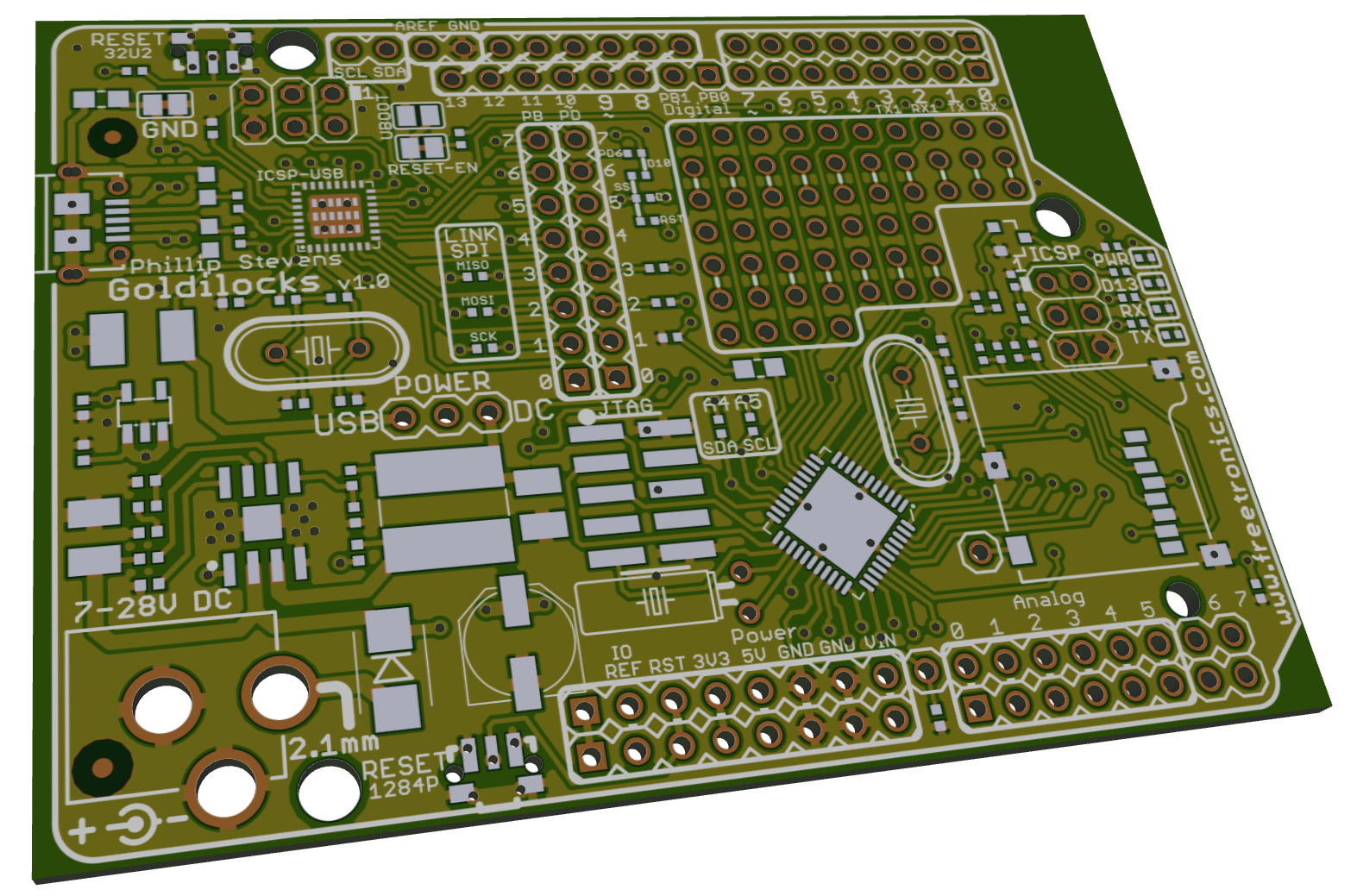
This is the final Goldilocks v1.1 board, that was prepared for Pozible Supporters.
Here are some screenshots of the prototype board design.
Differences between 328p and 1284p
The ATmega1284p has a number of significant differences from the 328p that make it a great MCU for the Arduino platform. Some are listed below, in no particular order.
16kByte SRAM = 8x Uno SRAM
The 1284p has 8x more SRAM than the 328p, and also has double the SRAM of the 2560. There is no other AVR ATmega MCU with this much SRAM.
For Ethernet, video, and USB applications where large frame buffers need to be maintained or manipulated, the flexibility of having 16kByte of SRAM will change the kind of applications that can be implemented.
4x Uno Flash & 2x Uno EEPROM
The 1284p has 4x more Flash and 2x more EEPROM than the 328p and therefore can store larger programs and non-volatile data.
2x Programmable USART
The 1284p has 2 programmable USARTs. These appear on Digital pin 0,1 and 2,3. This allows users to maintain the serial monitor connection with the Arduino IDE, whilst addressing another application, such as a GPS device. For new users and experienced alike having two serial interfaces will be a big improvement.
Independent Analogue Platform (separate I2C bus pins)
Using the SMD package for the 1284p allows the board layout to implement a fully independent analogue platform. This is because the I2C bus pins are on a separate port to the ADC pins, and the ADC pins have no “alternate function” except for the PCINT function. Also separate AVCC and GND pins allow the analogue PA Port to be powered and grounded separately from the digital section of the MCU.
Timer 3 (Extra 16bit timer)
The 1284p has an extra 16bit timer, Timer 3, that is not present on any other ATmega MCU. Timer 3 does not have PWM outputs (unlike Timer 0, Timer 1, and Timer 2), and therefore is free to use as a powerful internal Tick counter, for example in a RTOS. freeRTOS has already been modified to utilise this Timer 3.Timer 3 (Extra 16bit timer)
Timer 2 (Real Time Clock Oscillator)
The 1284p has a 32.768 kHz capable timer, that can be fitted with an accurate watch crystal to enable real time keeping. Use of the avr-libc time.h functionality (present only in upstream release currently) allows an efficient SystemTick to match with advance time and date functions.
JTAG Interface
The 1284p implements a JTAG functionality which will allow advanced developers the option to debug their code.
Better PWM access
The 1284p brings additional 8bit Timer 2 PWM outputs onto PD, which creates the option for 2 additional PWM options on this port. It also removes the sharing of the important 16bit PWM pins with the SPI interface, by moving them to PD4 & PD5, thus simplifying interface assignments.
Extra I/O pins (e.g. for internal SS pins)
The 1284p has additional digital I/O pins on the PB port. These pins could be utilised for on-board Slave Select pins (for example), without stealing on-header digital pins and freeing the Arduino Pin 10 for Shield SPI SS use exclusively.
Design Improvements on “Uno”
Add through-holes for all I/O
The existing Freetronics 2011 has space for prototyping, but doesn’t make any allowance for connecting pins to the prototyping space. Trying to solder jumpers between the I/O pins on the board backside is not very pretty, and also not robust for permanent prototyping. The Arduino Uno or Leonardo doesn’t have any prototyping space at all.
Suggest to include a row of through-holes inside the each of the pin headers to allow a header or jumper to be soldered to the I/O lead effectively.
Align the rows of through-holes to the 1/10” pitch, and to prototyping area pin pitch, to allow “Goldilocks” to have header pins soldered on the bottom, and be inserted into a standard breadboard.
Replicate SPI and I2C to through-holes (with additional 1284p Alternate SS I/O).
The SPI and I2C interfaces are used for many daughter card options (from Sparkfun for example). Some examples include RTC, acceleration & magnetic sensors.
These mini-cards need access to the SPI or I2C interfaces which are shared with I/O pins. Bringing these SPI and I2C pins with Vcc and GND onto through-holes in the standard order (of Sparkfun cards, for example) at the left and right ends (respectively) of the prototyping area would simplify prototyping with these interfaces.
This is now implemented on the Arduino Uno Rev 3. as additional pins for I2C.
But, the additional through-holes remain valuable for the prototyping area.
Add JTAG Interface
Adding a standard JTAG interface at the edge of the card would allow in circuit debugging to be implemented. Whilst there may not be sufficient space to implement a standard JTAG connector, there would be space to bring the JTAG pins onto through-holes for headers.
Add a Micro SD Cage
There is space to add the long term storage capability brought by an integral Micro SD Card cage. Many projects require logging of sensor data, or capturing or playback of information, and the Micro SD card format is the easiest way to get data onto and off of any format of PC or Smartphone. The ATmega1284p also has plenty of SRAM to allow large buffers for reading and writing to the Micro SD card, so it makes sense to include it as a most needed option.
Link ATmega32u2 and ATmega1284p SPI interfaces
The USB-serial interface on the Uno is implemented by a ATmega16u2 device, but its SPI bus is only connected to the SPI programming header, and the SS pin is not even brought out. The Goldilocks will allow the ATmega32u2 MOSI, MISO, CLK, pins to to be easily bridged (solder pads on rear of board), and bring the SS pins of both ATmega devices to a patch pad. This will allow the two devices to work in concert for demanding multi-processing applications, involving USB and other peripherals.
For some applications digital noise and voltage droop (when using servo PWM), can have a significant impact on the accuracy of ADC conversions. Using the SMD 1284p it is possible to completely electrically isolate the digital Vcc and analogue AVcc and GND planes, as well as isolating the ADC converter within the MCU. A separate rectifier, or low pass filter could be used to provide AVcc.
The option to bridge the 1284p I2C pins on SDA and SCL with A4 and A5, where needed for compatibility with Arduino Shields, should be maintained through the use of solder bridges.
Move Reset to edge
It is more common to need to use the Reset button with a shield in place, and if the Reset button is placed close to the edge (even vertically mounted, like the Seeed ADK main board), it can still be reached with a fingernail. Arduino Uno R3 implements this by moving Reset to the upper edge, near the USB connector.
Clock at 20MHz (or 22.1184MHz)
There is little reason to continue to run the MCU at 16MHZ, and given the MCU is specified to 20MHZ, being able to do 5 things, where previously we could only do 4, seems like a worthwhile improvement. Also, the use of a through hole precision crystal (not a SMD resonator) allows the use of after-market timing choices, eg 22.1184MHz for more accurate UART timings.
Design
This is the Goldilocks v1.0 prototype.
This is a proposal to map the ATmega1284p pins to the Arduino physical platform.
Arduino
UNO R3
328p Feature
328p Pin
1284p Pin
1284p Feature
Comment
Analog 0
PC0
PA0
Analog 1
PC1
PA1
Analog 2
PC2
PA2
Analog 3
PC3
PA3
Analog 4
SDA
PC4
PA4
PC1 I2C -> Bridged
Analog 5
SCL
PC5
PA5
PC0 I2C -> Bridged
Reset
Reset
PC6
RESET
Separate Pin
Digital 0
RX
PD0
PDO
RX0
Digital 1
TX
PD1
PD1
TX0
Digital 2
INT0
PD2
PD2
INT0 / RX1
Xtra USART1
Digital 3
INT1 / PWM2
PD3
PD3
INT1 / TX1
Xtra USART1
Digital 4
PD4
PD4
PWM1
16bit PWM
Digital 5
PWM0
PD5
PD5
PWM1
16bit PWM
Digital 6
PWM0
PD6
PD6
PWM2
Digital 7
PD7
PD7
PWM2
Digital 8
PB0
PB2
INT2
Xtra External Interrupt -> ATmega32u2 x-pad
Digital 9
PWM1
PB1
PB3
PWM0
Digital 10
SS / PWM1
PB2
PB4
SS / PWM0
SPI -> ATmega32u2 x-pad
Digital 11
MOSI / PWM2
PB3
PB5
MOSI
SPI
Digital 12
MISO
PB4
PB6
MISO
SPI
Digital 13
SCK
PB5
PB7
SCK
SPI
(Digital 14)
PB0
-> SDCard SPI SS
(Digital 15)
PB1
-> SDCard Card Sense
SCL
PC0
SCL
I2C – Separate
SDA
PC1
SDA
I2C – Separate
PC2
TCK
JTAG
PC3
TMS
JTAG
PC4
TDO
JTAG
PC5
TDI
JTAG
XTAL1
PB6
PC6
TOSC1
Unused
XTAL2
PB7
PC7
TOSC2
Unused
(Analog 6)
PA6
Unused -> Pad / Hole
(Analog 7)
PA7
Unused -> Pad / Hole
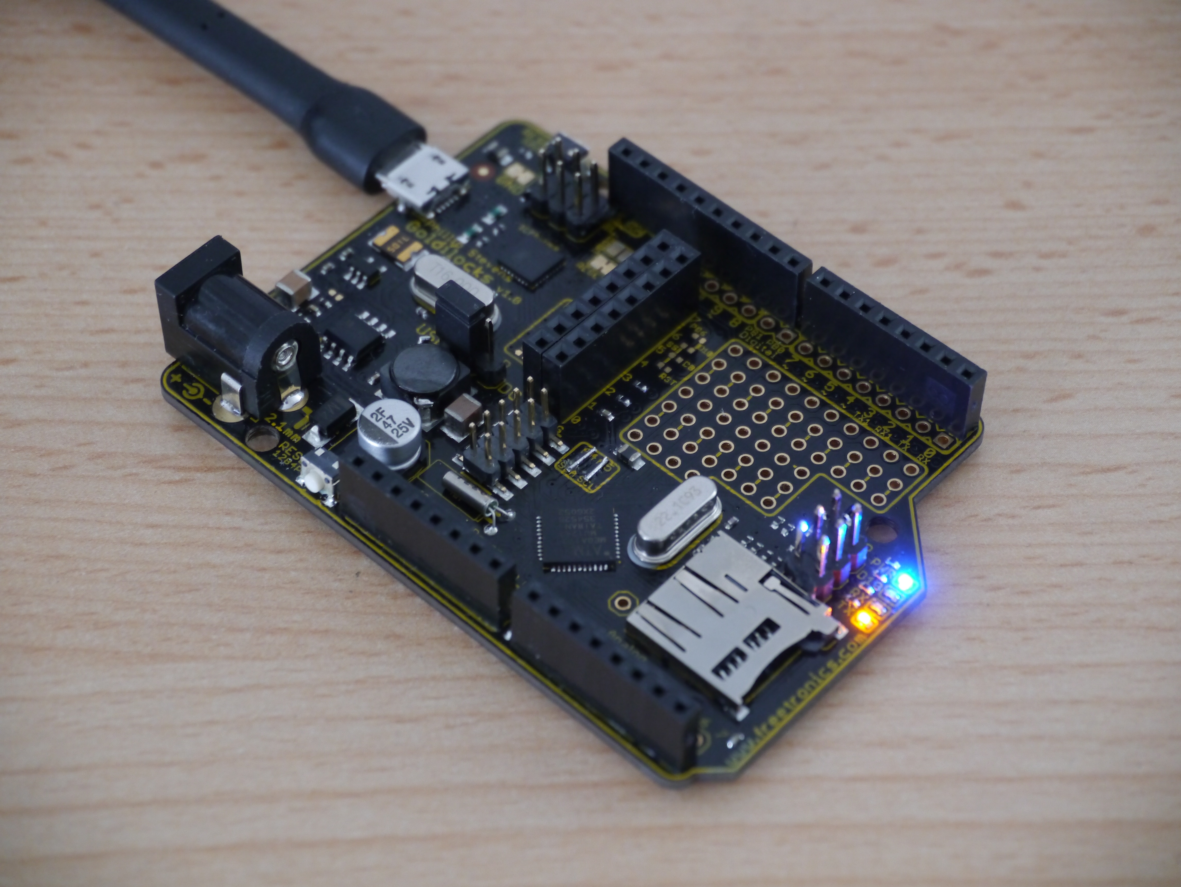
Here’s a picture of one of the two prototype boards, where I have added some additional items. I have changed the 1284p crystal to 22.1184MHz, and added a 5ppm 32kHz watch crystal for testing the avr-libc provided time.h functions.
Also I added header sockets for the 32u2 so that I could test its ability to program the 1284p using the LUFA AVRISP code, and determine how much decoupling should be added to the SPI bus link option. This is to ensure that even if the SPI bus is linked between the two MCU, that the 32u2 can’t lock up the SPI bus for devices trying to talk to the 1284p.
Also, I’ve added bridges for the SCL/SDA pins to the A4/A5 pins for old format (pre R3) shields.
I’ve prepared a preliminary distribution of the entire code set for goldilocks, including the lufa 130313 code used in the 32u2 and the stk500v2 bootloader used in the 1284p. This code is laid out in the arduino manner, with the directories matching the usual layout of Arduino boards.
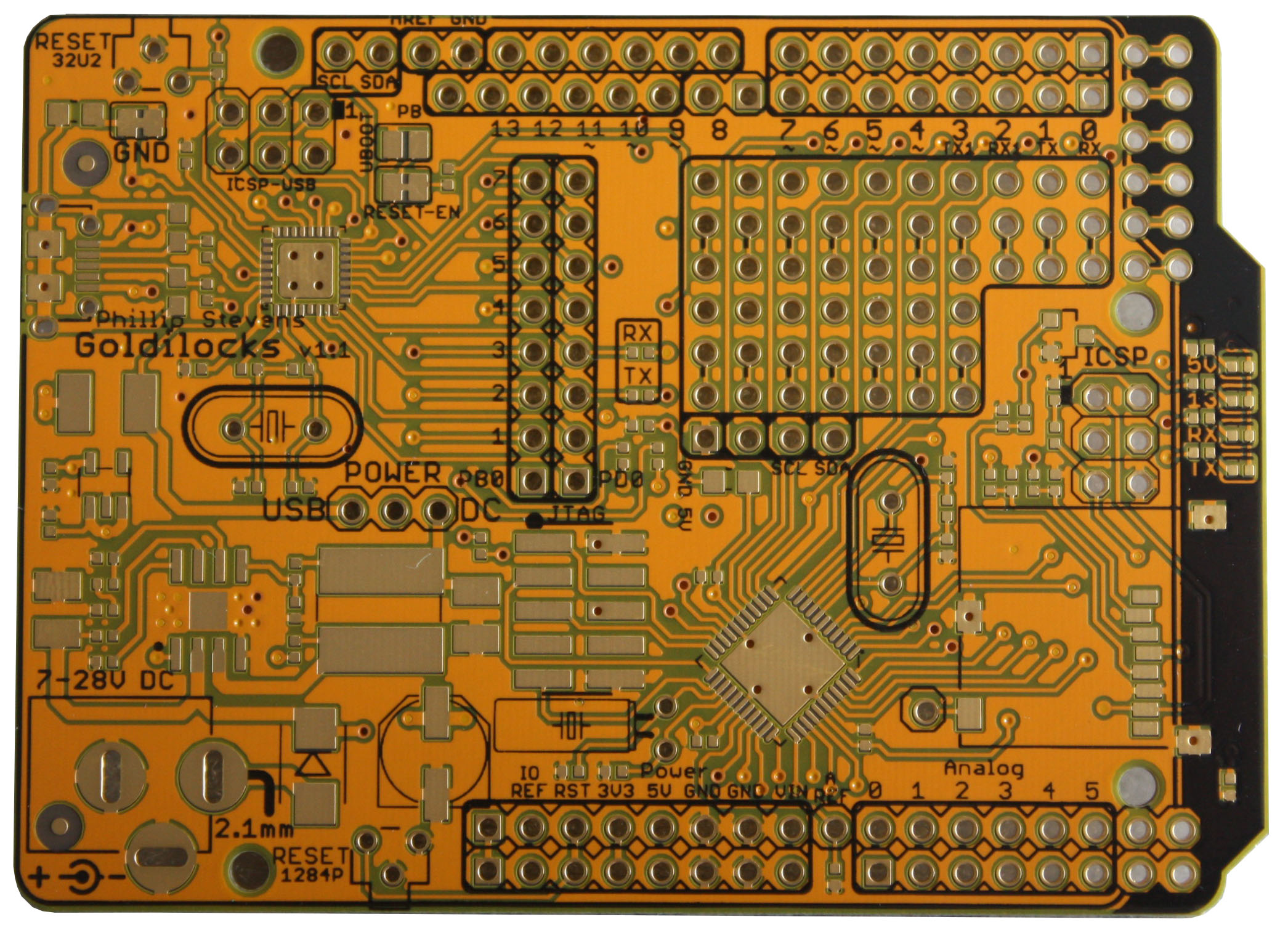
The production board design was finalised on June 28th and sent for manufacturing. The v1.1 production boards are shown below. Pick and place pictures soon.
Goldilocks v1.1 PCB Front
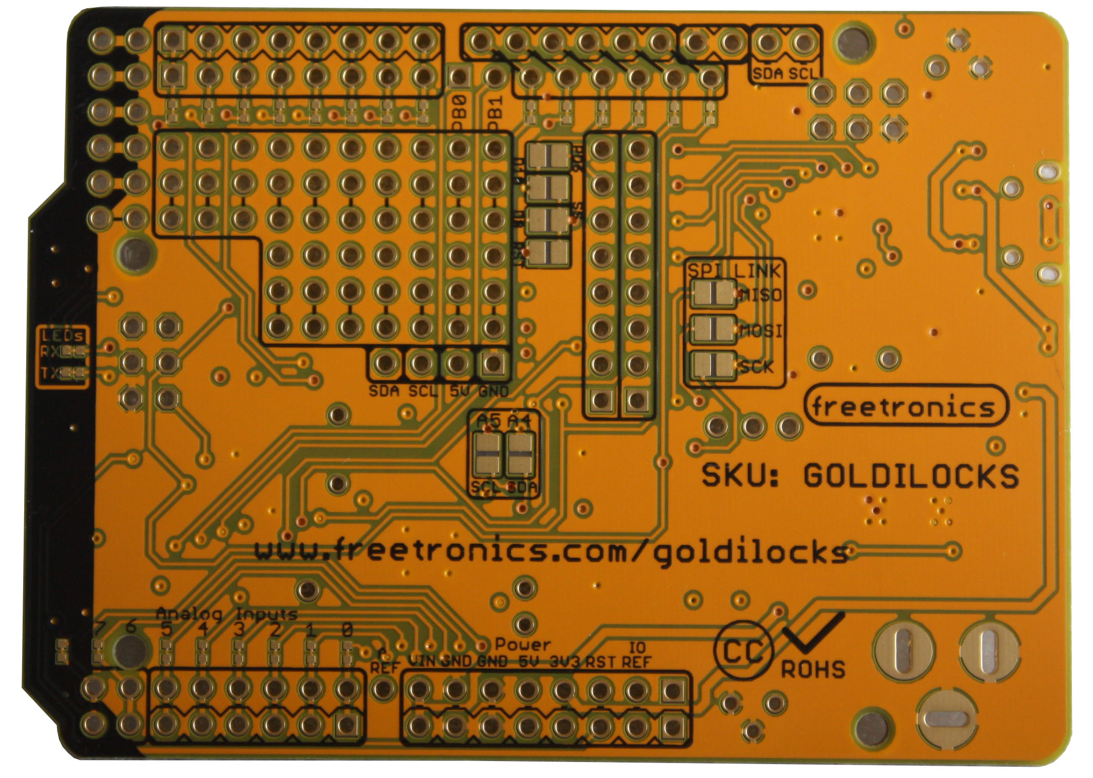
Goldilocks v1.1 PCB Back
Firmware
Moved support to the Arduino IDE Boards Manager.
Recompiled bootloader binaries with avr-gcc 4.9.2.
Returned to the original 2013 pins_arduino.h pin numbering, now that analogRead() issues are corrected.
It is not every day that I get to tell the family I’m doing “rocket science”, but I hope over the past few days, it can be an exception. Space, the final frontier. In this case, it was a lack of space and the frontier it creates, that got me thinking.
I immediately thought that it would be great to build a distributed cache RAM system to support each of the ATmega328p “Arduino” Client nodes, using the XRAM capabilities of the ATmega2561 Supervisor node. So, I did.
Using this prototype system, each Arduino Client node now has sole access to 32kByte of XRAMFS in addition to their 2kByte of internal RAM.
Initial performance measured is 422kByte/s throughput for the swap function. In other words, half of the entire Arduino RAM can be swapped with the contents of XRAMFS in just 4.74ms.
In working with the Arduino hardware I’ve found that the severe limitation in RAM space causes constraints on what can be done. For example, Ethernet, USB and other modern applications need kBytes of buffer to be used effectively, and the ATmega328p used as the Arduino Uno platform supports a total of only 2kB RAM.
Using the Arduino Mega (or Android ADK hardware) has been the saviour of that situation for me, offering an identical environment, but 8kByte of RAM as a playground. And, most importantly, the ability to directly connect 0 wait-state external SRAM.
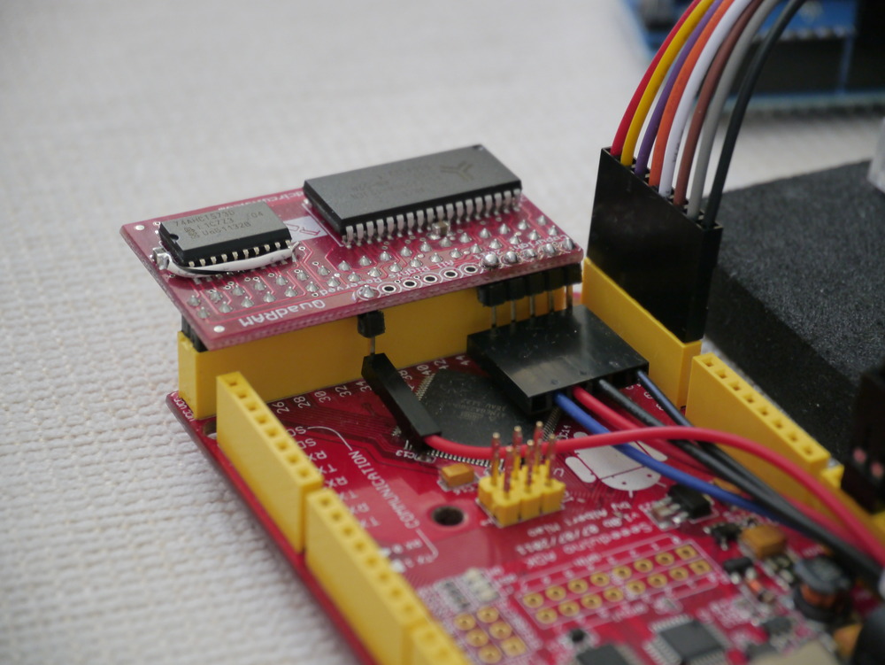
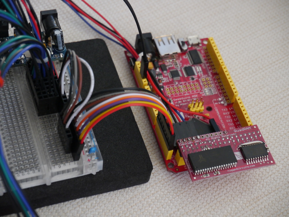
This XRAM capability of the ATmega2560 and ATmega2561 has been exploited by Rugged Circuits in their QuadRam module, which offers 512kByte of SRAM in one small package.
Therefore, using common off the shelf technology, I had the materials available to test the theory that building a XRAMFS system, to support the ArduSat platform, would work.
This allows each ArduSat Client to store 16 TIMES more data than it can currently access, and have access to that data at a relatively high speed from a medium not subject to wear (such as for example an SD card).
Ingredients & Build
This section looks at the ingredients and how to construct the prototype.
The ArduSat Supervisor node is based on the ATmega2561 MCU, because it is significantly smaller than the ATmega2560 MCU used in the Arduino Mega platform. The only difference between the two chips is that the ATmega2561 doesn’t provide as many Ports, and has only 64 Pins versus 100 Pins on the ATmega2560.
For this prototyping, the ATmega2560 is necessary, because I elected to use pin change interrupts as part of the bus protocol. Also, the Arduino Mega platform is readily available. I don’t even know where I’d go to get a ATmega2561 board…
The use of rainbow hook-up wire was essential for the success of the prototype.
Client Node – Arduino Uno / Freetronics Eleven
The ArduSat Client node is designed to be identical to the Arduino Uno platform, to ensure that it is absolutely easy for people to test code they intend to run in space. Therefore a variety of Arduino Uno devices are being used (basically, whatever I had around).
XRAM Module – Rugged Circuits QuadRAM
I’ve implemented using the Rugged Circuits QuadRAM and the MegaRAMpreviously. These modules slip over the end of the Arduino Mega platform, instantly enabling either 512kByte or 128kByte of zero wait state SRAM, mapped to the system address space. They also conveniently bring out the SPI interface onto through-hole for pins.
Something about the ability to create 16x 32kByte XRAM pages, linked with 16x Client nodes, seemed like synchronicity.
Layout
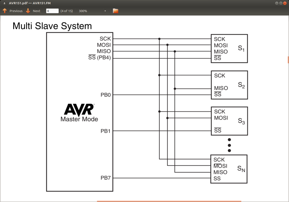
The prototype platform is designed to be the classic multi-slave SPI bus layout. This design is demonstrated in the AVR151 document and, in excerpt, is produced below.
Because of my decision to use the Pin Change Interrupts as part of the bus protocol, The Supervisor node (SPI Master) would use the Port K and Port J pins to fill the role of individual Slave Select (SS) pins. The Client nodes would each use their normal SS pin (PB2) to connect to the Supervisor.
In designing for 16x Client nodes, there is a limitation on Port J in that the good folks at Arduino determined not to break out all of the pins which, together with sharing PCINT8 with the Rx0 pin, significantly limits the number of Clients feasible on the prototype platform.
In practice, 8 Client nodes attached to all the pins on Pork K is the simple alternative. As luck (or good planning) would have it, those pins are all brought out onto one connector on the Arduino Mega platform, as evidenced by these pictures.
Amongst friends, a direct connection of the SPI SCK, MISO, and MOSI lines to all Clients is optimal. But in a shared environment, it would make sense to use FET bus isolation to keep Clients from physically attaching to the SPI bus until their SS line is held low by the Supervisor. A gram of hardware prevention can cure a tonne of software ill, as a “rogue” Client could otherwise potentially lock up the SPI bus for all, and the guys in the ISS won’t be happy if asked to hit the reset button.
Bus Protocol
Hey! – Yeah What? – This! – OK
That’s the protocol. Works in the home. Works in the office. Works the world over.
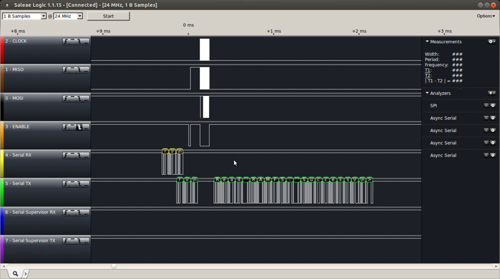
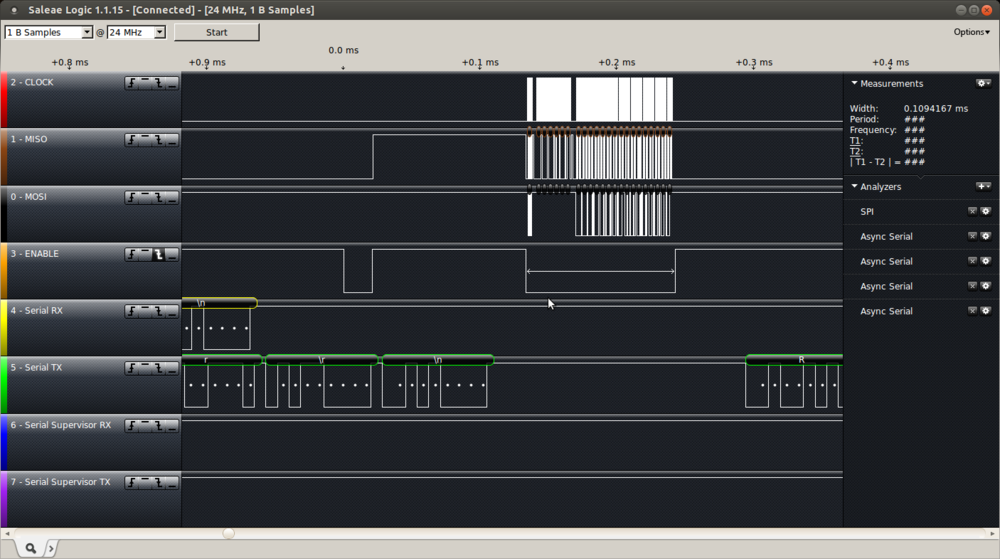
Information to this Saleae Logic chart below in Client Implementation section.
Hey!
The Supervisor node holds all the PCINT pins high. If a Client wants to initiate a Read/Write/Swap transaction, it will pull its SS line low for 30µs. This needs to be long enough for the Supervisor to register an interrupt and process it. If multiple Clients call out simultaneously, no problem, the Supervisor will grab all of the requests and push them onto a queue of requests to serve.
Yeah What?
At the next opportunity, the Supervisor serving task will pop a request off the queue, and identify which Client made the request. It will also check if there were other simultaneous requests, and push them back to the front of the queue.
The Supervisor then pulls the relevant Client SS line low. The Client has been listening for this, and at this point it enables its Slave interface to the SPI bus, and the two swap acknowledgements. When the Supervisor receives the ACK code, it knows the Client is ready, so it requests a command.
This!
When the Client (SPI Slave) has received the Supervisor ACK code, it prepares a command, and is prepared to either read, write or swap XRAMFS data under the command of the Supervisor (SPI Master).
The command set implemented by this protocol can be easily extended to include accessing other shared resources connected to the Supervisor node. This could include analogue sensors, SDCARD mass storage (though using the SPI bus would offer a degree of complexity), or serial interfaced devices.
OK
At the end of one command, with the data transaction complete, a final byte is exchanged to ensure that the Client has remained in sync with the Supervisor, and the SPI bus is released by the Client. It is important the Client stays off the SPI bus. The Supervisor then processes the next Yeah What? request.
Supervisor Implementation – freeRTOS
The Supervisor is implemented as a freeRTOS task, using standard SPI bus libraries contained in my code base. These libraries (now that this project has worked them over) are about as optimised as is possible to write in C, and achieve a good throughput over the SPI bus.
There are two (or one) PCINT based Interrupt that reads the PCINT pins and pushes the raw pin state onto a queue. This process traps multiple simultaneous requests, overcoming any interrupt masking or race conditions. Currently 30µs are allowed for the interrupts to execute. 10µs has been tested, but depending on how long the Supervisor stays in “Critical” state (interrupts off) processing other (non XRAMFS) tasks this time can be adjusted.
From idle, the Supervisor takes only 90µs to 0.1ms to pop a request from the queue and action it. Under load, it could take as long as 64ms to action a request. As soon as the pin state is collected it is processed to identify which SS line triggered the call, and therefore which bank of XRAM should be enabled. Also, at this time I check that no additional requests are pending from the same pin state. If so, the remaining pin state is pushed back on the queue to get next time round.
The exchange of acknowledgements ensures that both sides are speaking SPI, and are set to proceed.
The command contains the action (read / write / swap / test), the address of the XRAMFS block, the size of the XRAMFS block, and a CRC byte.
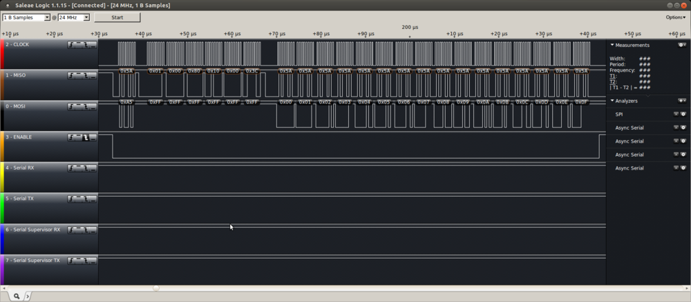
The bus transaction speed is dependent on the SPI Master SCK clock divisor. Optimally, a SPI Slave can receive data at 1/4th of its system clock. Currently, it is set to one 1/8th, therefore theoretical performance is double that of the logic capture above.
Initially, I determined to calculate a CRC byte to store along with the data, but the calculation time is large compared to the transaction time, and therefore too costly to implement at the protocol level. The application should utilise the CRC when it recovers data to confirm that the data is intact, and not irradiated.
Also, error checking following the transfer could be implemented. But at this stage I think it is better to have the Client do all sanity and error checking of its own data.
Client Implementation – freeRTOS or Arduino IDE
The Client is implemented in freeRTOS as a simple library function, that is passed a command structure, and a pointer to local RAM to be Read/Write/Swap. Some details below.
typedef enum { Huh        = 0, // Client didn't issue us a command, so just break.
               Read       = 1, // read from XRAMFS
               Write      = 2, // write to XRAMFS
               Swap       = 3, // read from both XRAMFS & local RAM, and swap
               Test       = 4  // do something else, to be determined
} RAMFSCommand; // from point of view of the client (Arduino 328p)

typedef struct        /* structure to hold the RAMFS info */
{ RAMFSCommand       ram_cmd;        // Read / Write / Swap / Test
  size_t             ram_addr;       // Address of first byte of RAM in a RAMFS (greater than RAM_START_ADDR)
  uint16_t           ram_size;       // Size of RAM block in RAMFS (less than RAM_COUNT or 32kByte)
  uint8_t            ram_crc8;       // Calculated CRC of stored data
} xRAMFSarray, * pRAMFSarray;

uint8_t ramfs_transfer_block( pRAMFSarray pRAMFS_block, uint8_t *data );
I used C and the freeRTOS platform because it is easiest for my environment, and I know it best. But, I’ll re-write it as a library in the Arduino IDE environment as needed. It won’t be too hard.
The client can use the XRAMFS malloc function to manage RAM allocation. A very simple malloc has been built, which can’t free XRAMFS. But, it can be simply ignored if desired and the command structure can be filled manually.
Initially, I implemented an interrupt driven semaphore system to manage the Yeah What? part of the bus protocol, but typically the Supervisor responds so quickly that the time to do several context swaps generated by the interrupt exceeded the time the Supervisor was prepared to wait. A simple wait loop keeps the Client on ready standby for 90µs so it can complete the transaction in the shortest time.
The Client code has no knowledge of where its XRAM is located on the Supervisor. Therefore the code is orthogonal and constant, irrespective which Client being used. This is a very useful feature where the author may not know in advance which ArduSat Client his code will be running upon.
Client application code should be written to make use of the Swap XRAMFS <-> RAM capability. This makes best use of the SPI bus features to combine Read and Write into one transaction, effectively doubling throughput over the Write plus Read combination.
The user interface (monitor) is just for initial testing. I’ll have to write a load generation rig to find out what this baby can do, but that can wait for the next post. The logic analyser has captured the result of the > r (read) command in the below command line sequence. We can see the 20µs (now 30µs) Hey! on the Slave Select, 90µs pass before the acknowledgement bytes are swapped (only one cycle needed), 6 bytes of command structure are passed (Read command is 0x01), and then the data is read out of XRAMFS to the Client.
Design Notes
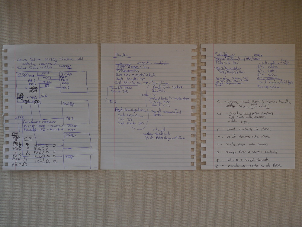
The basis of every design: detailed functional specifications, hardware design, and user interface documentation. Oh, and scribbles much.
Updates
I’ve updated the code on 22 February to remove some oversights in the Client main program, and added the OK check byte to the protocol. Code as usual on AVRfreeRTOS on Sourceforge.
Updated on 23 February to include some error checking on Supervisor side (preventing malicious Client requests), and on Client side preventing hang if the Supervisor is AWOL. Also removed the aggressive SPI timing utilising receive double buffering, as it often caused errors, and had no performance effect.
Initial performance measured is about 422kByte/s throughput for the swap function. Specifically 4.73825ms is needed for a complete 2048Byte data payload transaction (including sync, command, & OK timing). This also includes freeRTOS task swapping, as the Supervisor task is run with interrupts enabled in normal mode.
Have fixed some code issues on 4 March, mainly around a few µs delays required to let things run their course.
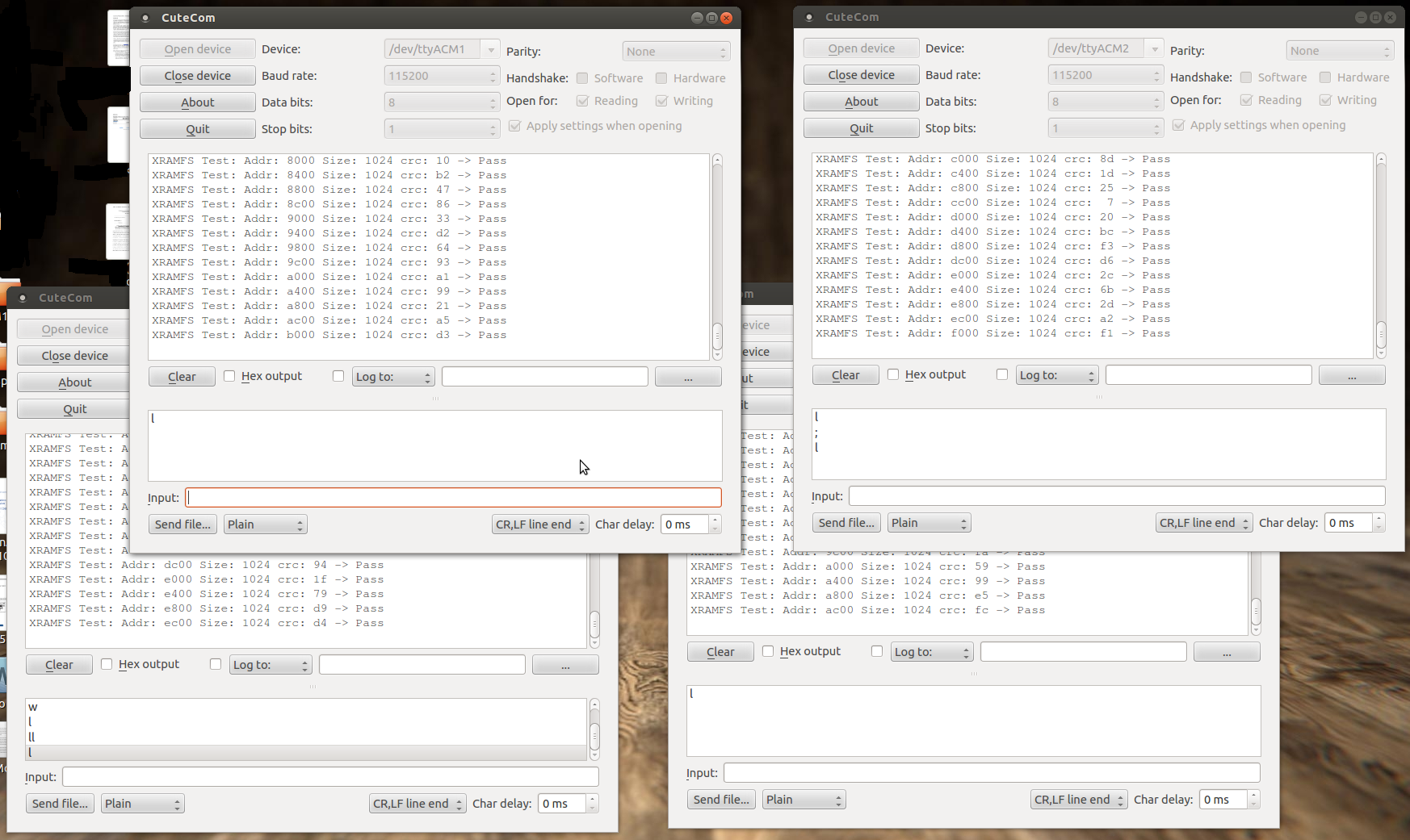
Now the platform is running stable with 4x Clients. A video is here