ArduSat SD Card Prototyping

Since my last post on the ArduSat and the idea I had to use the Supervisor node, an ATmega2561, as the core of a centralised eXtended RAM system for the Client nodes, ATmega328p “Arduino” devices, I’ve been thinking and working on a solution for building a centralised non-volatile SD Card based storage solution.

With design, sometimes it is necessary to let an idea stew for a while before the right answer just sort of distils out of the soup. For the solution for this problem, this was the case. There was some thinking space required…

thinking space

The Question

There are 16 Client nodes in the ArduSat platform. Each and any of them may wish to use the central SD Card to store information at the same, or at different times. How would it be possible to allow more than 16 files to be open on the one SD Card (connected to the Supervisor node) whilst maintaining consistency in the file system? How would access to the file system be scheduled?

The Tools

I have been using the ChaN FatFs file system libraries now for some time. They are fully featured and have a very clean design, fully separating the file system layer from the underlying physical media access layer (the drivers). This means that the file system tools can be implemented on many different architectures, with only changes to the driver layer (DiskIO) needed for each platform.

The Thought Process

My initial thought was that the Supervisor node should maintain the file system, and that I should write packaging for the FatFs file system commands to allow them to be remotely implemented across the SPI bus, in a similar manner as described in the XRAMFS post.

The idea of writing these “remote controls” for the file system commands was scary, as I recognised that there are 33 commands in the interface, and each of them has their own characteristics. Also, maintaining these interfaces would likely be problematic, as I would have to test each command extensively to ensure that there were no “thick thumb” errors introduced into the stable and proven FatFs library.

Some weeks passed…

Then at about 3am, I realised that the right answer was to write a “shim” between the standard FatF file system commands and the standard physical media drivers, and to have this shim operate across the SPI bus in exactly the same manner as the XRAMFS solution.

So, I wrote it.

The Solution

The solution separates the ChaN libraries into two parts. The file system part is resident on the Client node. Each Client node maintains its own view of the file system on the Supervisor SD Card. As the ChaN FatFs library is written for low memory devices, the file directory tree is refreshed each time a change in the working file is done. The Supervisor node only does the DiskIO under the command of each of the Clients.

There are only 5 relevant driver layer DiskIO commands. These commands are used in the Supervisor node to execute requests sent over the SPI bus from the individual Clients. Since there are only a small number of commands, and they are static and dependent on the architecture of the machine they’re running on, their functionality is quite constant. The Supervisor has no knowledge of the file system at all. It simply implements DiskIO commands on sectors of the SD Card as requested, one a time, as requested by Clients.

The Supervisor implementation simply expands on the existing Task loop established for the XRAMFS system, by adding in the 5 additional DiskIO commands. The added complexity, that the SD Card is accessed over the SAME SPI bus as the communications between Client and Supervisor, means that I had to introduce an interim “Pending” state for commands to allow the Client to wait for confirmation that a task has been completed or, in the case of disk_read or disk_ioctl, to recover the waiting data from the Supervisor.

The Client implementation inserts different shim DiskIO commands for the FatF system to call. These commands use the SPI bus to call the Supervisor, and enter a request. Some commands return immediately, allowing the Supervisor to continue with the command, once the command and any required data has been transferred. Other commands wait until they can retrieve information from the Supervisor, before returning to the FatF file system layer of the library.

In this solution, the XRAMFS was instrumental in simplifying the transfer of information. The exclusive availability of 16kB of RAM for each Client meant that disk_write or disk_read commands could cache their data in XRAMFS whilst it was actually written to or read from the SDCard. Because the RAM is available exclusively, there is no consideration that another Client may overwrite the results of a command, or that memory exhaustion may corrupt data.

The code is available at Sourceforge in the usual location.

How does it work?

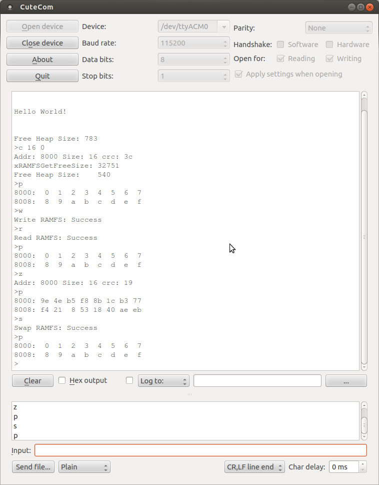
When a Client program calls one of the FatFs library commands, it in turn calls one of the special ArduSat SPI DiskIO shim routines. These routines signal the Supervisor in the normal manner, and transfer any data associated with the command into the Page of XRAMFS assigned to the Client.

The Supervisor will then undertake the standard DiskIO command, retaining the result of the command and any data resulting from the command in XRAMFS.

Both Client DiskIO routines, and the Task running in the Supervisor are aware of the “Pending” state, which is where a DiskIO command has been completed on the Supervisor and there is data waiting in the XRAMFS for the Client to recover.

Once the Client DiskIO command completes, it returns the normal interface information to the calling FatFs command.

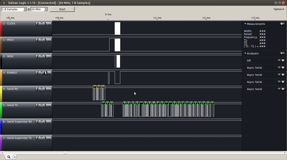
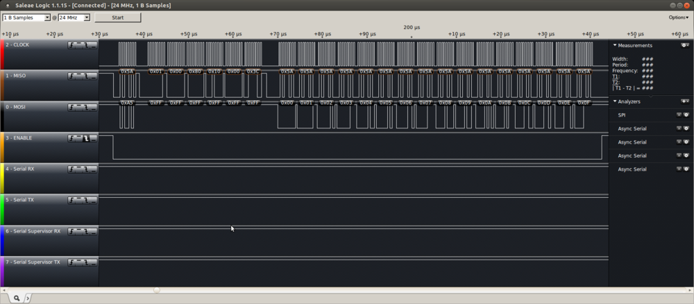
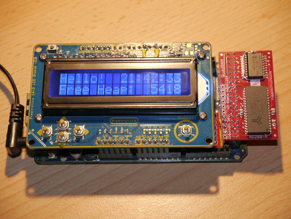
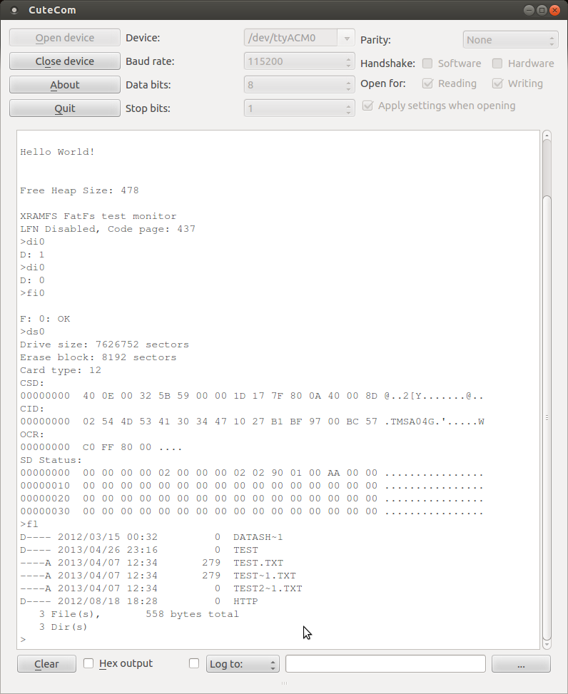
Here a monitor program on a Client is initialising the SD Card. If the Supervisor notices that the SD Card is not initialised, it will return Error, and then undertake to initialise the card. The second call for initialisation will then be successful. This decoupling method ensures that Clients cannot reinitialise the card, whilst other Clients may be using the Card.

The file system (on the Client) is then initialised Then, the SD Card status is read. Finally, the current working directory is read and printed.

Initialisation

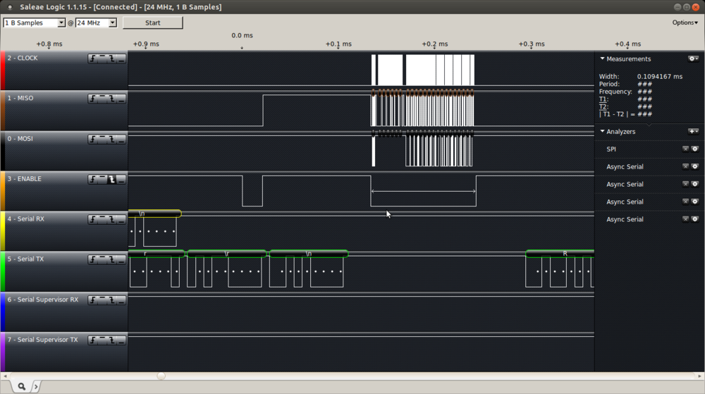
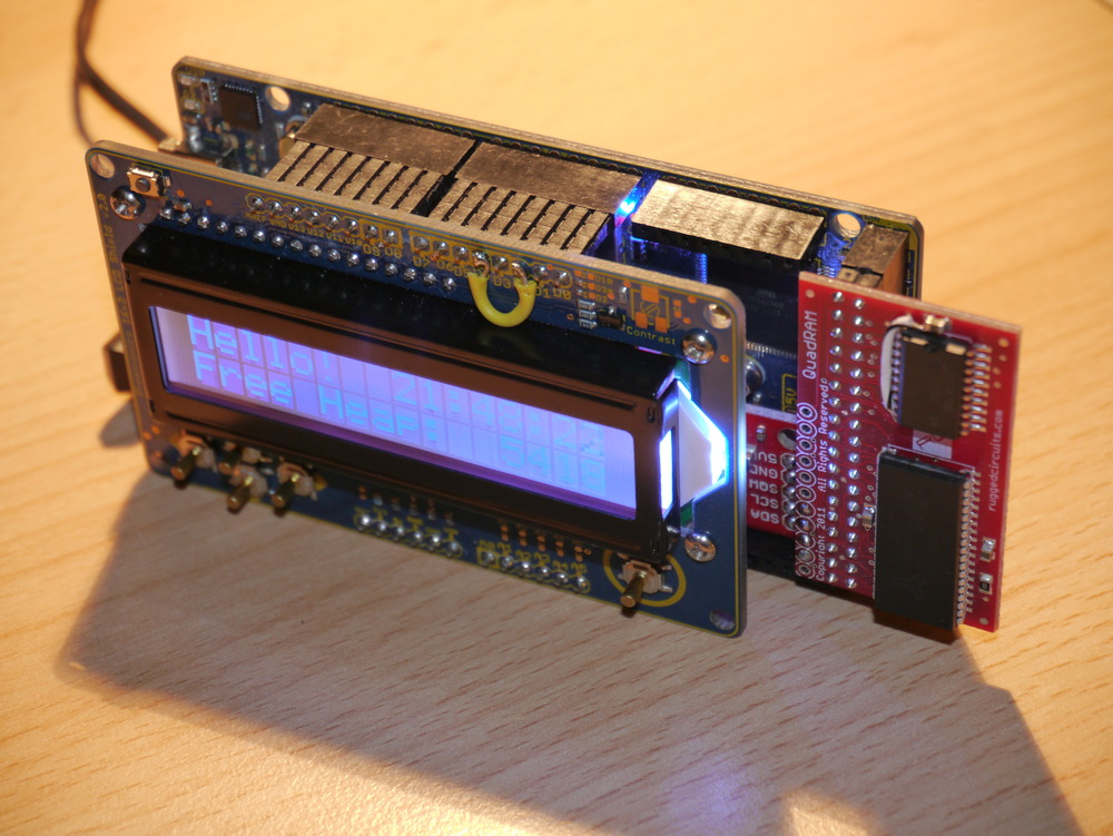
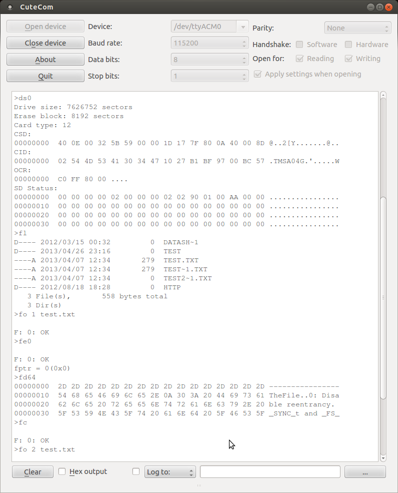
In this screenshot, a file is opened for reading, and the file pointer set to the start of the file. A dump of the first 64 Bytes of the file is read and printed. Then the file is closed.

readfile

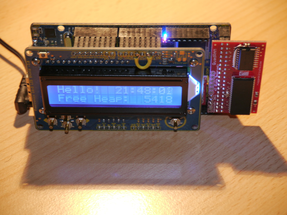
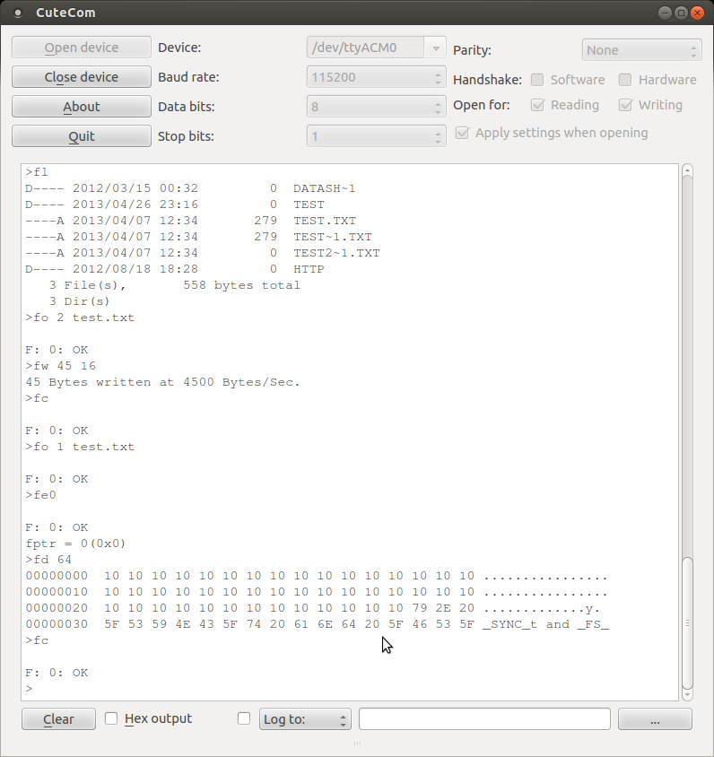
Here, the same file as above is opened for writing, and 45 bytes of 0x10 (16) are being written. The result is checked by opening the file for reading, and dumping the relevant bytes to the screen. Success!

writefile

Issues

The Client (Arduino) ATmega328p has so little Flash and RAM that implementing the FatFs consumes a significant proportion of the available resources. From the ChaN FatFs web site, at least 13 kByte of Flash (of 32 kByte on the Arduino), and 600 Bytes of RAM (of 2048 Bytes on the Arduino) are consumed by the library alone. This is excluding the working buffers necessary to prepare or process data for storage.

I was unable to fully test the FatFs solution, because of RAM and Flash limitations. I simply couldn’t turn on all the features. However, I have some confidence that the solution fully works, because the actual FatFs library is unchanged from the working solution that I’ve tested on the Arduino Mega platform. It is only the DiskIO routines that have been tampered with, and since they produce reliable results for some of the FatFs functions, there is every reason to believe they would work for all of the functions.

Thank you

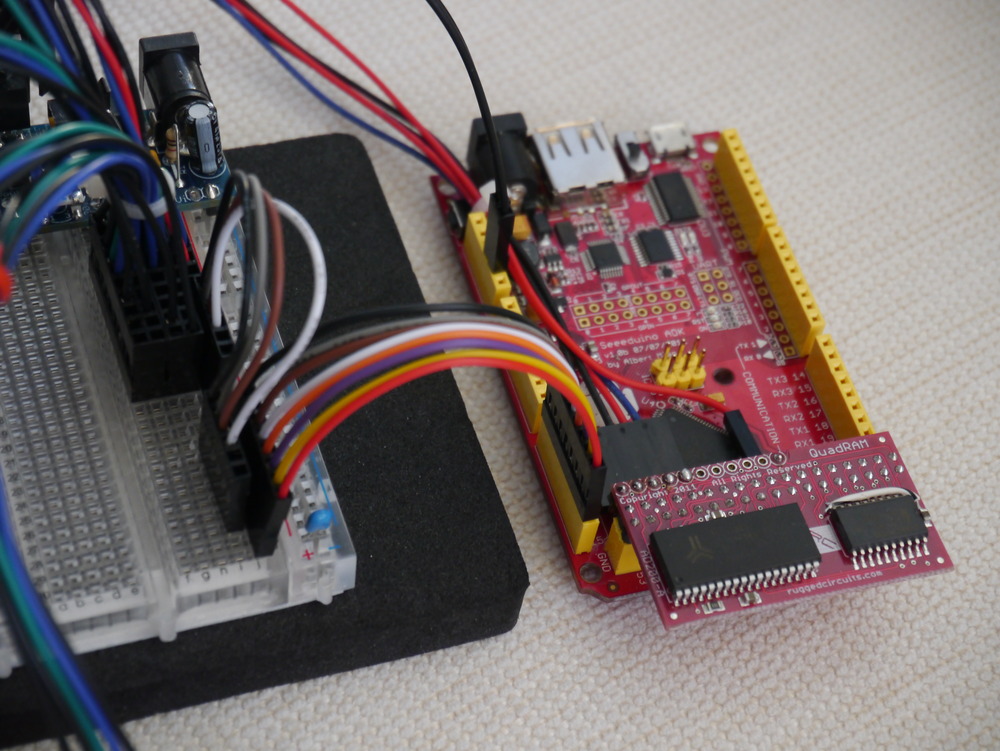
Jon for providing a new Freetronics EtherMega, so that I could complete the prototyping work.

ArduSat and NanoSatisfi for running a great project, which inspired this thought process. Possibly, this work might be useful for one of the launches over the coming years.

Another NBN rant

There are a couple of things that the NBN fanbois generally fail to note about Liberal Party Broadband Policy.
(and I don’t vote, so this is just a technical & economic discussion)

It is not about FTTN at all. FTTN is only a cheap and fast “filler” for areas of Australia that aren’t being done some other way.

  • Satellite remains.
  • Fixed wireless remains.
  • Greenfield FTTH remains.
  • FTTH On-demand (i.e. anyone who wants to have it) remains.
  • HFC (and we know that EuroDOCSIS can do 1Gb/s services, as needed) will be recovered and provide service for 2.6 million homes, immediately.

All that is changing is that the difficult brownfields services are being given a fast and cheap alternative to get some kind of service upgrade in the short term (say 5 to 8 years).

Fanbois bitch about the FTTN cabinets in the street. Yes they’re ugly. Essentially, they’re providing centralised networked power to drive the copper tail for all FTTN subscribers. Cabinets are ugly, but they’re very maintainable, and upgradable at low cost and with low impact for consumers. The current FTTH solution is putting an unmaintainable ugly lead acid battery IN MY LOUNGEROOM! (And, forcing me to pay for the power for their service too. I’m used to getting my POTS power for free.)

And, if (when) the FTTH battery is dead my lifeline services are affected. It is part of every NBNCo service agreement that it is not their liability, if your battery is dead, you can’t make a call, and therefore you die!

I’d rather have someone professional maintaining my (mother’s / great aunt’s / disabled friend’s) lifeline services battery and have it somewhere where it can be properly maintained to deliver a known grade of service, without interfering with my life.

Oh, and the famous diagram with 1Gb/s FTTH services on it, with everything else miles below. Nice picture. He could have added HFC services up there at 1Gb/s too, but he didn’t. But paying for these 1Gb/s services is another story.

The NBNCo has gazetted their 100Mb/s prices in a SAU with the ACCC, and their prices will be INCREASED annually by CPI (-1.5%) for 27 YEARS. That means in 27 years we’ll be paying much more than today (compound it up, I dare you) for the same service. They need to lock in this price to pay for their network. Don’t imagine that Moore’s law is going to apply here. 27 years ago was 1986, and then 9600 baud was looking pretty good. How will 100Mb/s look in 2040? Now, how much is then 1Gb/s going to cost, if 100Mb/s has a fixed price for the next 27 years? Good question. You got any unwanted children you can sell?

UPDATE: So just a day after this rant was written, NBNCo announced pricing for 1Gb/s services, conveniently only available after the next election in December 2013. Pricing is $150 wholesale. This is exactly twice the 100Mb/s price. An interesting price point, given this will cut the fan-out on the GPON network infrastructure from 32:1 down to 2:1. Also RSPs will need to upgrade their POI backhaul packages by a factor of 10x if they want to provide this service. Using the ACCC transmission pricing calculator, this looks like a recipe for a VERY expensive retail service.

The Labour NBN plan is unbuildable. There are not the fibre splicers in the country we need to achieve the required daily rate build rate. NBN Co contractors (to get their contracts in the first place) are paying lowest rates in the market. Anyone with any skills is working on the mines in WA, fly in fly out. Not camping in the truck, schlepping around the country digging trenches. This was apparent back in 2010. Blind Freddy could have predicted the situation the NBNCo is in now, with missed delivery targets.

In 15 years, Conroy might be remembered for the man who thought of NBN. But Turnbull will be remembered as the one who saved it, and delivered it.
(Actually, Conroy should be remembered as the man who killed NBN, when he axed its predecessor OPEL http://en.wikipedia.org/wiki/OPEL_Networks, on April 2, 2008, when he entered office).

UPDATE: So on 12th July 2013, Mike Quigley resigned or retired from his role as CEO of NBN Co. Surely his efforts will not go unrewarded. My bet is that in the second half of 2014 or early 2015 Mr Quigley will be appointed to the Board of Alcatel Lucent. After all, getting your former employer an uncontested 1,500 million Dollar contract from the Australian Government for obsolete GPON equipment must be worth something, right?

On which tool to use and when

Recently, I’ve been thinking about tools and what to use as my preferred “platform” for this hobby I call hacking. Actually, I’ve been worrying about this since October 2011, when I first wrote the proposal for the Goldilocks, my project for building a 1284p based Arduino Uno clone.

In 2011, I had tried to build several projects utilising uIP and other IP stacks (W5100 Arduino Ethernet), and RFID and uSDCard FatFS support as some of the foundations. I found that the Arduino Uno simply didn’t allow me to do anything requiring complex libraries, because it lacked RAM resources. Because of these issues, I tried two things. Firstly, I started using the Arduino Mega platform, and I also tried to use ARM based platforms with Arduino physical compatibility (e.g. Maple, Teensy, kl25z). Also, people have commented, why not use a RaspberryPi or BeagleBone as the platform for your projects, they are cheap and 50 times more capable than the Arduino Uno.

I wasted a lot of time in 2012 looking at how to achieve what I want to learn, without actually getting much satisfaction. Each one of the noted suggestions has issues, but the key issue is always complexity. I keep on coming back to the AVR ATmega 8 bit platform as the right answer. These notes are my attempt to discuss (justify) why I think that may apply for others too.

My interest lies in working with a soldering iron (hardware) and a compiler, and understanding how software interacts with the physical world. The ability to directly and explicitly influence the state of a pin on a micro-controller, either in C language or in assembler is the point of the exercise. Being able to interact with physical devices, through low level bus protocols, such as SPI or I2C, or standards, such as servo-motor timing or TCP/IP, enables me to understand what the sensors, motors, and actuators of the world really do.

Many platforms attempt to abstract away the “complexity” of dealing with these issues, and give their users the power to achieve much more in short periods of time with high level languages such as Python, or JavaScript. These languages give their users rich platforms which can quickly integrate into web applications. That in itself is a great thing, but it is simply not what interests me.

The key advantage of the AVR ATmega platform is that the platform is absolutely mature, completely open, and is very scalable. The power of the ability to compile and link a simple C program with avr-gcc, and upload it to an AVR with avrdude (either with a bootloader, or SPI interface) cannot overstated. These tools with avr-libc make the AVR ATmega platform very easy to love, and easy to scale with.

In comparison, the ARM based platforms mentioned, as well as others I’ve not mentioned, suffer from a very fragmented approach to library availability, support from the C compiler, and proprietary approaches uploading compiled code. Specifically, each ARM platform seems to need to have its own libraries and linker scripts and, because of the nature of the ARM licencing, each platform may have different capabilities and ways of servicing its hardware interfaces. All very confusing for me at least.

So why not use a RaspberryPi or a BeagleBoard? Well whilst both of these are great platforms (which I also own and use), they are normally used with a full scale Linux based operating system. Having the systematic overhead of a Hardware Abstraction Layer, and device driver interfaces just takes away the purity of simple one machine instruction equals one physical outcome.

I guess what I’m saying that one day I’ll migrate to ARM based 32 bit systems for this kind of enjoyment, but that day is not today.

“Goldilocks” 1284p Arduino UNO Clone

The Pozible project for Goldilocks boards is funded and closed.
Pozible Goldilocks

As featured in Make.

Freetronics Goldilocks is now sold out.
Freetronics Goldilocks

But, Freetronics are considering making a new version.
Please add your wish list here.

Also, I’m working on a new version, Goldilocks Analogue with an integrated dual channel DAC. Now a second prototype of the Goldilocks Analogue has been designed and tested. It has taken a year, because I’ve been using the existing Goldilocks boards for a number of projects. Now I’m designing (hopefully) the final iteration of the Goldilocks Analogue before it goes into production.

I have a Kickstarter project to get the Goldilocks Analogue into production. The project was successfully funded.

I sell on Tindie

Updated Firmware for Goldilocks (Pozible & Freetronics)

  •  LUFA 140928 for ATmega32u2 DFU and for U2duino (USB to USART).
  • Increased bootloader timeout for ATmega1284p.
  • Updated IDE file structure to provide support for Arduino IDE 1.6.x.
  • Renumbered I/O pins for greater commonality with Arduino core.
  • Also added a Goldilocks Analogue Bootloader, running at 24.576MHz

Look for Goldilocks in the Unofficial Boards Support List, and follow the instructions in the Goldilocks Analogue User Manual.

Background

This proposal is to implement an Arduino clone using the ATmega1284p MCU, as replacement for the normal ATmega328p MCU, bringing significant improvements and longevity into the existing Arduino platform.

The current Arduino Uno and Leonardo devices cater for many applications, but they are becoming limited for some modern applications, such as Ethernet networking, SD Card storage, and USB based systems. The limitation in SRAM in the 328p and 32u4 is the most apparent issue, and this is the most difficult to supplement with external components. The Uno R3 platform is too small for demanding applications, and therefore not the right solution.

Arduino Mega devices are available which provide more RAM (but still less than Goldilocks) and many more interface pins, but unfortunately many of the standard Arduino Shields will not work with the Mega, unless you are prepared to hack them. The Mega platform is too big for the standard Shields, and therefore not the right solution.

Arduino and others are moving towards 32 bit MCU devices, including ARM Cortex based platforms such as the Arduino Due, which brings significantly more resource into play, but these platforms will require a major re-education of  users, and may actually fragment the Arduino user group. Also, these ARM processor based devices must be operated at 3.3V and can only supply 4mA per I/O, which makes them incompatible with many of the existing Arduino Shields.

I believe the Goldilocks solution is to use the Arduino Uno / Leonardo R3 physical format, for 100% Arduino Shield compatibility at 5V and with the standard pin layout. But using the ATmega1284p processor to provide significant improvements in RAM, FLASH, EEPROM, interfaces, and other factors.

I’ve been working with Arduino devices now for some years, and have found that my interest remains in fully understanding the way the “bare metal” processor is working. The Arduino platform gives me that opportunity.
https://sourceforge.net/projects/avrfreertos/

Whilst many argue that the days of 8 bit processors are numbered, and that devices such as the Raspberry Pi are the future, I would say that there remains a need for very simple, but very capable platforms, such as the “Goldilocks” platform proposed here. Raspberry Pi and others are essentially Linux machines, and are addressing different needs to this platform.

The 1284p MCU has already been used by the RepRap project as a platform in their minimalist Arduino platform, as a result of them experiencing similar resource limitation issues. The RepRap 1284p platform maintains Arduino code compatibility (boot-loader, board descriptions, avrdude) but abandons physical compatibility, as theirs is a special purpose application and has no need to support Arduino Shields.

http://www.kirbyand.co.uk/serendipity/index.php?/pages/Min644pWarez.html
http://www.kirbyand.co.uk/serendipity/index.php?/pages/min644p.html

Similarly Pololu use the 1284p in their Orangutan SVP platform, but again theirs is a special application, which incorporates many robotics interfaces, and deviates from both the Arduino physical and software platform. Pololu also implement an on-board ISP, which removes the need for the Arduino serial bootloader freeing more space for program code.

http://www.pololu.com/catalog/product/1327

Recently, others are starting to use the 1284p as the “Goldilocks” solution between 328p and 2560. This helps with establishing the precedent for the “Goldilocks” with the Arduino IDE and its hardware descriptions.
http://maniacbug.wordpress.com/2011/11/27/arduino-on-atmega1284p-4/
http://arduino.cc/forum/index.php/topic,64612.0.html
http://blog.stevemarple.co.uk/2011/11/calunium-pcb-version.html
http://www.bajdi.com/bajduino/bajduino-1284/
http://forum.freetronics.com/viewtopic.php?f=6&t=330

This is the final Goldilocks v1.1 board, that was prepared for Pozible Supporters.

Goldilocks 20MHz PCB

Here are some screenshots of the prototype board design.

Goldilocks Front Side

Differences between 328p and 1284p

The ATmega1284p has a number of significant differences from the 328p that make it a great MCU for the Arduino platform. Some are listed below, in no particular order.

  • 16kByte SRAM = 8x Uno SRAM

The 1284p has 8x more SRAM than the 328p, and also has double the SRAM of the 2560. There is no other AVR ATmega MCU with this much SRAM.

For Ethernet, video, and USB applications where large frame buffers need to be maintained or manipulated, the flexibility of having 16kByte of SRAM will change the kind of applications that can be implemented.

  • 4x Uno Flash & 2x Uno EEPROM

The 1284p has 4x more Flash and 2x more EEPROM than the 328p and therefore can store larger programs and non-volatile data. 

  • 2x Programmable USART

The 1284p has 2 programmable USARTs. These appear on Digital pin 0,1 and 2,3. This allows users to maintain the serial monitor connection with the Arduino IDE, whilst addressing another application, such as a GPS device. For new users and experienced alike having two serial interfaces will be a big improvement. 

  • Independent Analogue Platform (separate I2C bus pins)

Using the SMD package for the 1284p allows the board layout to implement a fully independent analogue platform. This is because the I2C bus pins are on a separate port to the ADC pins, and the ADC pins have no “alternate function” except for the PCINT function. Also separate AVCC and GND pins allow the analogue PA Port to be powered and grounded separately from the digital section of the MCU.

  • Timer 3 (Extra 16bit timer)

The 1284p has an extra 16bit timer, Timer 3, that is not present on any other ATmega MCU. Timer 3 does not have PWM outputs (unlike Timer 0, Timer 1, and Timer 2), and therefore is free to use as a powerful internal Tick counter, for example in a RTOS. freeRTOS has already been modified to utilise this Timer 3. Timer 3 (Extra 16bit timer)

  • Timer 2 (Real Time Clock Oscillator)

The 1284p has a 32.768 kHz capable timer, that can be fitted with an accurate watch crystal to enable real time keeping. Use of the avr-libc time.h functionality (present only in upstream release currently) allows an efficient SystemTick to match with advance time and date functions.

  • JTAG Interface

The 1284p implements a JTAG functionality which will allow advanced developers the option to debug their code.

  • Better PWM access

The 1284p brings additional 8bit Timer 2 PWM outputs onto PD, which creates the option for 2 additional PWM options on this port. It also removes the sharing of the important 16bit PWM pins with the SPI interface, by moving them to PD4 & PD5, thus simplifying interface assignments. 

  • Extra I/O pins (e.g. for internal SS pins)

The 1284p has additional digital I/O pins on the PB port. These pins could be utilised for on-board Slave Select pins (for example), without stealing on-header digital pins and freeing the Arduino Pin 10 for Shield SPI SS use exclusively.

Design Improvements on “Uno”

  • Add through-holes for all I/O

The existing Freetronics 2011 has space for prototyping, but doesn’t make any allowance for connecting pins to the prototyping space. Trying to solder jumpers between the I/O pins on the board backside is not very pretty, and also not robust for permanent prototyping. The Arduino Uno or Leonardo doesn’t have any prototyping space at all.

Suggest to include a row of through-holes inside the each of the pin headers to allow a header or jumper to be soldered to the I/O lead effectively.

Align the rows of through-holes to the 1/10” pitch, and to prototyping area pin pitch, to allow “Goldilocks” to have header pins soldered on the bottom, and be inserted into a standard breadboard.

  • Replicate SPI and I2C  to through-holes (with additional 1284p Alternate SS I/O).

The SPI and I2C interfaces are used for many daughter card options (from Sparkfun for example). Some examples include RTC, acceleration & magnetic sensors.

These mini-cards need access to the SPI or I2C interfaces which are shared with I/O pins. Bringing these SPI and I2C pins with Vcc and GND onto through-holes in the standard order (of Sparkfun cards, for example) at the left and right ends (respectively) of the prototyping area would simplify prototyping with these interfaces.

This is now implemented on the Arduino Uno Rev 3. as additional pins for I2C.

http://www.arduino.cc/en/Main/arduinoBoardUno

But, the additional through-holes remain valuable for the prototyping area.

  • Add JTAG Interface

Adding a standard JTAG interface at the edge of the card would allow in circuit debugging to be implemented. Whilst there may not be sufficient space to implement a standard JTAG connector, there would be space to bring the JTAG pins onto through-holes for headers.

  • Add a Micro SD Cage

There is space to add the long term storage capability brought by an integral Micro SD Card cage. Many projects require logging of sensor data, or capturing or playback of information, and the Micro SD card format is the easiest way to get data onto and off of any format of PC or Smartphone. The ATmega1284p also has plenty of SRAM to allow large buffers for reading and writing to the Micro SD card, so it makes sense to include it as a most needed option.

  • Link ATmega32u2 and ATmega1284p SPI interfaces

The USB-serial interface on the Uno is implemented by a ATmega16u2 device, but its SPI bus is only connected to the SPI programming header, and the SS pin is not even brought out. The Goldilocks will allow the ATmega32u2 MOSI, MISO, CLK, pins to to be easily bridged (solder pads on rear of board), and bring the SS pins of both ATmega devices to a patch pad. This will allow the two devices to work in concert for demanding multi-processing applications, involving USB and other peripherals.

  • Isolate analogue platform (optional SCL & SDA bridge)

For some applications digital noise and voltage droop (when using servo PWM), can have a significant impact on the accuracy of ADC conversions. Using the SMD 1284p it is possible to completely electrically isolate the digital Vcc and analogue AVcc and GND planes, as well as isolating the ADC converter within the MCU. A separate rectifier, or low pass filter could be used to provide AVcc.

The option to bridge the 1284p I2C pins on SDA and SCL with A4 and A5, where needed for compatibility with Arduino Shields, should be maintained through the use of solder bridges. 

  • Move Reset to edge

It is more common to need to use the Reset button with a shield in place, and if the Reset button is placed close to the edge (even vertically mounted, like the Seeed ADK main board), it can still be reached with a fingernail. Arduino Uno R3 implements this by moving Reset to the upper edge, near the USB connector.

  • Clock at 20MHz (or 22.1184MHz)

There is little reason to continue to run the MCU at 16MHZ, and given the MCU is specified to 20MHZ, being able to do 5 things, where previously we could only do 4, seems like a worthwhile improvement. Also, the use of a through hole precision crystal (not a SMD resonator) allows the use of after-market timing choices, eg 22.1184MHz for more accurate UART timings.

Design

This is the Goldilocks v1.0 prototype.

GOLDILOCKS-prototype-top

This is a proposal to map the ATmega1284p pins to the Arduino physical platform.

Arduino
UNO R3
328p Feature 328p Pin 1284p Pin 1284p Feature Comment
Analog 0 PC0 PA0
Analog 1 PC1 PA1
Analog 2 PC2 PA2
Analog 3 PC3 PA3
Analog 4 SDA PC4 PA4 PC1 I2C -> Bridged
Analog 5 SCL PC5 PA5 PC0 I2C -> Bridged
Reset Reset PC6 RESET Separate Pin
Digital 0 RX PD0 PDO RX0
Digital 1 TX PD1 PD1 TX0
Digital 2 INT0 PD2 PD2 INT0 / RX1 Xtra USART1
Digital 3 INT1 / PWM2 PD3 PD3 INT1 / TX1 Xtra USART1
Digital 4 PD4 PD4 PWM1 16bit PWM
Digital 5 PWM0 PD5 PD5 PWM1 16bit PWM
Digital 6 PWM0 PD6 PD6 PWM2
Digital 7 PD7 PD7 PWM2
Digital 8 PB0 PB2 INT2 Xtra External Interrupt
-> ATmega32u2 x-pad
Digital 9 PWM1 PB1 PB3 PWM0
Digital 10 SS / PWM1 PB2 PB4 SS / PWM0 SPI
-> ATmega32u2 x-pad
Digital 11 MOSI / PWM2 PB3 PB5 MOSI SPI
Digital 12 MISO PB4 PB6 MISO SPI
Digital 13 SCK PB5 PB7 SCK SPI
 (Digital 14) PB0 -> SDCard SPI SS
 (Digital 15) PB1 -> SDCard Card Sense
SCL PC0 SCL I2C – Separate
SDA PC1 SDA I2C – Separate
PC2 TCK JTAG
PC3 TMS JTAG
PC4 TDO JTAG
PC5 TDI JTAG
XTAL1 PB6 PC6 TOSC1 Unused
XTAL2 PB7 PC7 TOSC2 Unused
 (Analog 6) PA6 Unused -> Pad / Hole
 (Analog 7) PA7 Unused -> Pad / Hole

Here’s a picture of one of the two prototype boards, where I have added some additional items. I have changed the 1284p crystal to 22.1184MHz, and added a 5ppm 32kHz watch crystal for testing the avr-libc provided time.h functions.

Also I added header sockets for the 32u2 so that I could test its ability to program the 1284p using the LUFA AVRISP code, and determine how much decoupling should be added to the SPI bus link option. This is to ensure that even if the SPI bus is linked between the two MCU, that the 32u2 can’t lock up the SPI bus for devices trying to talk to the 1284p.

Also, I’ve added bridges for the SCL/SDA pins to the A4/A5 pins for old format (pre R3) shields.

P1030259

I’ve prepared a preliminary distribution of the entire code set for goldilocks, including the lufa 130313 code used in the 32u2 and the stk500v2 bootloader used in the 1284p. This code is laid out in the arduino manner, with the directories matching the usual layout of Arduino boards.

The production board design was finalised on June 28th and sent for manufacturing. The v1.1 production boards are shown below. Pick and place pictures soon.

Goldilocks v1.1 PCB Front

Goldilocks v1.1 PCB Front

Goldilocks v1.1 PCB Back

Goldilocks v1.1 PCB Back

Firmware

Moved support to the Arduino IDE Boards Manager.

Recompiled bootloader binaries with avr-gcc 4.9.2.

Returned to the original 2013 pins_arduino.h pin numbering, now that analogRead() issues are corrected.

Look for Goldilocks in the Unofficial Boards Support List, and follow the instructions in the Goldilocks Analogue User Manual.

Support for Arduino IDE 1.6.x.

Increased 1284p bootloader time out to 4 seconds.

Set upload speed to 38400 (single speed UART) for Goldilocks Analogue.

Goldilocks_20160108 Files

Support for Arduino IDE 1.5.x. Updated to LUFA 140928 for DFU and U2duino for 32u2.

No change for 1284p. Added Goldilocks Analogue bootloader, but no LUFA required because of FTDI USB interface.

Updated directory structure to support Arduino IDE 1.5.x. Modified pins_arduino.h to support analogRead() correctly.

Goldilocks 20150101 Files

Updated to LUFA 130901 for DFU and U2duino for 32u2. No change for 1284p.

Goldilocks 20130918 Files

Obsolete – Fixed USART mismatch by adjusting stk500v2 bootloader to 38,400 baud.

Goldilocks 20130818 Files

Obsolete – Fixed 32U2 tristate RESET issue.

Goldilocks 20130814 Files

Obsolete – Fixed stk500v2 bootloader monitor issues and included compiled firmware files.

Goldilocks 20130605 Files

Obsolete – Initial release.

Goldilocks 20130601 Files

ArduSat XRAMFS Prototyping

It is not every day that I get to tell the family I’m doing “rocket science”, but I hope over the past few days, it can be an exception. Space, the final frontier. In this case, it was a lack of space and the frontier it creates, that got me thinking.

At the recent Linux Conf AU Jon Oxer spoke about Freetronics’ efforts in designing the payload for the upcoming NanoSatisfi ArduSat1 launch (pictured below). Jon mentioned in the presentation that the AVR freeRTOS code compilation that I’ve been supporting is being used in the Supervisor node of that platform.

Ardusat_payload_freetronics

I immediately thought that it would be great to build a distributed cache RAM system to support each of the ATmega328p “Arduino” Client nodes, using the XRAM capabilities of the ATmega2561 Supervisor node. So, I did.

P1030071
P1030068

Using this prototype system, each Arduino Client node now has sole access to 32kByte of XRAMFS in addition to their 2kByte of internal RAM.

Initial performance measured is 422kByte/s throughput for the swap function. In other words, half of the entire Arduino RAM can be swapped with the contents of XRAMFS in just 4.74ms.

I’ve also the code for supporting a centralised SD Card on this platform to Sourceforge AVRfreeRTOS, and written about it at ArduSat SD Card Prototyping.

Background

In working with the Arduino hardware I’ve found that the severe limitation in RAM space causes constraints on what can be done. For example, Ethernet, USB and other modern applications need kBytes of buffer to be used effectively, and the ATmega328p used as the Arduino Uno platform supports a total of only 2kB RAM.

Using the Arduino Mega (or Android ADK hardware) has been the saviour of that situation for me, offering an identical environment, but 8kByte of RAM as a playground. And, most importantly, the ability to directly connect 0 wait-state external SRAM.

This XRAM capability of the ATmega2560 and ATmega2561 has been exploited by Rugged Circuits in their QuadRam module, which offers 512kByte of SRAM in one small package.

P1030069

Therefore, using common off the shelf technology, I had the materials available to test the theory that building a XRAMFS system, to support the ArduSat platform, would work.

This allows each ArduSat Client to store 16 TIMES more data than it can currently access, and have access to that data at a relatively high speed from a medium not subject to wear (such as for example an SD card).

Ingredients & Build

This section looks at the ingredients and how to construct the prototype.

Supervisor Node – Arduino Mega / Freetronics EtherMega / Android ADK

The ArduSat Supervisor node is based on the ATmega2561 MCU, because it is significantly smaller than the ATmega2560 MCU used in the Arduino Mega platform. The only difference between the two chips is that the ATmega2561 doesn’t provide as many Ports, and has only 64 Pins versus 100 Pins on the ATmega2560.

P1030070

For this prototyping, the ATmega2560 is necessary, because I elected to use pin change interrupts as part of the bus protocol. Also, the Arduino Mega platform is readily available. I don’t even know where I’d go to get a ATmega2561 board…

The use of rainbow hook-up wire was essential for the success of the prototype.

Client Node – Arduino Uno / Freetronics Eleven

The ArduSat Client node is designed to be identical to the Arduino Uno platform, to ensure that it is absolutely easy for people to test code they intend to run in space. Therefore a variety of Arduino Uno devices are being used (basically, whatever I had around).

XRAM Module – Rugged Circuits QuadRAM

I’ve implemented using the Rugged Circuits QuadRAM and the MegaRAM previously. These modules slip over the end of the Arduino Mega platform, instantly enabling either 512kByte or 128kByte of zero wait state SRAM, mapped to the system address space. They also conveniently bring out the SPI interface onto through-hole for pins.

Ad200

Something about the ability to create 16x 32kByte XRAM pages, linked with 16x Client nodes, seemed like synchronicity.

Layout

The prototype platform is designed to be the classic multi-slave SPI bus layout. This design is demonstrated in the AVR151 document and, in excerpt, is produced below.

Spi_wiring

Because of my decision to use the Pin Change Interrupts as part of the bus protocol, The Supervisor node (SPI Master) would use the Port K and Port J pins to fill the role of individual Slave Select (SS) pins. The Client nodes would each use their normal SS pin (PB2) to connect to the Supervisor.

In designing for 16x Client nodes, there is a limitation on Port J in that the good folks at Arduino determined not to break out all of the pins which, together with sharing PCINT8 with the Rx0 pin, significantly limits the number of Clients feasible on the prototype platform.

In practice, 8 Client nodes attached to all the pins on Pork K is the simple alternative. As luck (or good planning) would have it, those pins are all brought out onto one connector on the Arduino Mega platform, as evidenced by these pictures.

Amongst friends, a direct connection of the SPI SCK, MISO, and MOSI lines to all Clients is optimal. But in a shared environment, it would make sense to use FET bus isolation to keep Clients from physically attaching to the SPI bus until their SS line is held low by the Supervisor. A gram of hardware prevention can cure a tonne of software ill, as a “rogue” Client could otherwise potentially lock up the SPI bus for all, and the guys in the ISS won’t be happy if asked to hit the reset button.

Bus Protocol

Hey! – Yeah What? – This! – OK

That’s the protocol. Works in the home. Works in the office. Works the world over.

Read_overviewRead_middleviewRead_detail

Information to this Saleae Logic chart below in Client Implementation section.

Hey!

The Supervisor node holds all the PCINT pins high. If a Client wants to initiate a Read/Write/Swap transaction, it will pull its SS line low for 30µs. This needs to be long enough for the Supervisor to register an interrupt and process it. If multiple Clients call out simultaneously, no problem, the Supervisor will grab all of the requests and push them onto a queue of requests to serve.

Yeah What?

At the next opportunity, the Supervisor serving task will pop a request off the queue, and identify which Client made the request. It will also check if there were other simultaneous requests, and push them back to the front of the queue.

The Supervisor then pulls the relevant Client SS line low. The Client has been listening for this, and at this point it enables its Slave interface to the SPI bus, and the two swap acknowledgements. When the Supervisor receives the ACK code, it knows the Client is ready, so it requests a command.

This!

When the Client (SPI Slave) has received the Supervisor ACK code, it prepares a command, and is prepared to either read, write or swap XRAMFS data under the command of the Supervisor (SPI Master).

The command set implemented by this protocol can be easily extended to include accessing other shared resources connected to the Supervisor node. This could include analogue sensors, SDCARD mass storage (though using the SPI bus would offer a degree of complexity), or serial interfaced devices.

OK

At the end of one command, with the data transaction complete, a final byte is exchanged to ensure that the Client has remained in sync with the Supervisor, and the SPI bus is released by the Client. It is important the Client stays off the SPI bus. The Supervisor then processes the next Yeah What? request.

Supervisor Implementation – freeRTOS

The Supervisor is implemented as a freeRTOS task, using standard SPI bus libraries contained in my code base. These libraries (now that this project has worked them over) are about as optimised as is possible to write in C, and achieve a good throughput over the SPI bus.

There are two (or one) PCINT based Interrupt that reads the PCINT pins and pushes the raw pin state onto a queue. This process traps multiple simultaneous requests, overcoming any interrupt masking or race conditions. Currently 30µs are allowed for the interrupts to execute. 10µs has been tested, but depending on how long the Supervisor stays in “Critical” state (interrupts off) processing other (non XRAMFS) tasks this time can be adjusted.

From idle, the Supervisor takes only 90µs to 0.1ms to pop a request from the queue and action it. Under load, it could take as long as 64ms to action a request. As soon as the pin state is collected it is processed to identify which SS line triggered the call, and therefore which bank of XRAM should be enabled. Also, at this time I check that no additional requests are pending from the same pin state. If so, the remaining pin state is pushed back on the queue to get next time round.

The exchange of acknowledgements ensures that both sides are speaking SPI, and are set to proceed.

The command contains the action (read / write / swap / test), the address of the XRAMFS block, the size of the XRAMFS block, and a CRC byte.

The bus transaction speed is dependent on the SPI Master SCK clock divisor. Optimally, a SPI Slave can receive data at 1/4th of its system clock. Currently, it is set to one 1/8th, therefore theoretical performance is double that of the logic capture above.

Initially, I determined to calculate a CRC byte to store along with the data, but the calculation time is large compared to the transaction time, and therefore too costly to implement at the protocol level. The application should utilise the CRC when it recovers data to confirm that the data is intact, and not irradiated.

Also, error checking following the transfer could be implemented. But at this stage I think it is better to have the Client do all sanity and error checking of its own data.

Client Implementation – freeRTOS or Arduino IDE

The Client is implemented in freeRTOS as a simple library function, that is passed a command structure, and a pointer to local RAM to be Read/Write/Swap. Some details below.

typedef enum { Huh        = 0, // Client didn't issue us a command, so just break.
               Read       = 1, // read from XRAMFS
               Write      = 2, // write to XRAMFS
               Swap       = 3, // read from both XRAMFS & local RAM, and swap
               Test       = 4  // do something else, to be determined
} RAMFSCommand; // from point of view of the client (Arduino 328p)

typedef struct        /* structure to hold the RAMFS info */
{ RAMFSCommand       ram_cmd;        // Read / Write / Swap / Test
  size_t             ram_addr;       // Address of first byte of RAM in a RAMFS (greater than RAM_START_ADDR)
  uint16_t           ram_size;       // Size of RAM block in RAMFS (less than RAM_COUNT or 32kByte)
  uint8_t            ram_crc8;       // Calculated CRC of stored data
} xRAMFSarray, * pRAMFSarray;

uint8_t ramfs_transfer_block( pRAMFSarray pRAMFS_block, uint8_t *data );

I used C and the freeRTOS platform because it is easiest for my environment, and I know it best. But, I’ll re-write it as a library in the Arduino IDE environment as needed. It won’t be too hard.

The client can use the XRAMFS malloc function to manage RAM allocation. A very simple malloc has been built, which can’t free XRAMFS. But, it can be simply ignored if desired and the command structure can be filled manually.

Initially, I implemented an interrupt driven semaphore system to manage the Yeah What? part of the bus protocol, but typically the Supervisor responds so quickly that the time to do several context swaps generated by the interrupt exceeded the time the Supervisor was prepared to wait. A simple wait loop keeps the Client on ready standby for 90µs so it can complete the transaction in the shortest time.

The Client code has no knowledge of where its XRAM is located on the Supervisor. Therefore the code is orthogonal and constant, irrespective which Client being used. This is a very useful feature where the author may not know in advance which ArduSat Client his code will be running upon.

Client application code should be written to make use of the Swap XRAMFS <-> RAM capability. This makes best use of the SPI bus features to combine Read and Write into one transaction, effectively doubling throughput over the Write plus Read combination.

The user interface (monitor) is just for initial testing. I’ll have to write a load generation rig to find out what this baby can do, but that can wait for the next post. The logic analyser has captured the result of the > r (read) command in the below command line sequence. We can see the 20µs (now 30µs) Hey! on the Slave Select, 90µs pass before the acknowledgement bytes are swapped (only one cycle needed), 6 bytes of command structure are passed (Read command is 0x01), and then the data is read out of XRAMFS to the Client.

Terminal

Design Notes

The basis of every design: detailed functional specifications, hardware design, and user interface documentation. Oh, and scribbles much.

P1030072

Updates

I’ve updated the code on 22 February to remove some oversights in the Client main program, and added the OK check byte to the protocol. Code as usual on AVRfreeRTOS on Sourceforge.

Updated on 23 February to include some error checking on Supervisor side (preventing malicious Client requests), and on Client side preventing hang if the Supervisor is AWOL. Also removed the aggressive SPI timing utilising receive double buffering, as it often caused errors, and had no performance effect.

Initial performance measured is about 422kByte/s throughput for the swap function. Specifically 4.73825ms is needed for a complete 2048Byte data payload transaction (including sync, command, & OK timing). This also includes freeRTOS task swapping, as the Supervisor task is run with interrupts enabled in normal mode.

Have fixed some code issues on 4 March, mainly around a few µs delays required to let things run their course.

Now the platform is running stable with 4x Clients. A video is here

And here is a screenshot of the 4x terminals.

4xXRAMFS Client Monitors Screenshot

April 27th – I’ve uploaded the code for supporting a centralised SD Card on this platform to Sourceforge AVRfreeRTOS, and written about it at ArduSat SD Card Prototyping.

VW Jetta Mk5 hacking – 5 year report

Well my peoples’ car has turned 5 years old. Manufactured in May 2007, and purchased in December 2007 for the express purpose of ferrying MissNow9 to school, it has performed admirably during its tenure as a shuttle bus.

Got it cleaned today, so perhaps it is time to write a review of its performance over the past years and to catalogue some of the minor improvements it has received.

Now, as a project, I think it is complete. So, it should get us to school in style for quite a few years to come.

Update October 2021

The car has been passed to a new owner, who has been making some further improvements as he desires. I guess this is the final update here.

Recently, he took it to the dyno to test and tune.

This slideshow requires JavaScript.

Update September 2017

In September 2017 the car finally passed 100,000km, and is approaching its 10th anniversary. Over the past 3 years it has seen fairly light usage (no school run, no track days), so the annual mileage has been fairly low. Perhaps because of this light usage, or because of the VW engineering capability, there have been no issues to speak of since this report was originally written, 5 years ago.

Input

This car started out as a VW Jetta MkV FSi 2.0 with DSG gearbox, leather seats, and alarm.

It looks very boring. It has a huge 527 litre boot. Largest of almost any car sold in Australia.

It is easy to park, and it is easy to drive. Cheap to own.

P1020938

But, it is actually a Golf GTI in disguise. It has a very nice turbo petrol motor producing 147 kW (200 hp) for motivation, and something like 47 controllers on its CAN bus to manage everything electrical.

Design specification

  1. Always remain reliable – to get to school on time.
  2. Look completely boring – stay inside OEM visual envelope.
  3. Rock on the race track – be very surprising for drivers of track-day sports cars.

Outcome

Jetta – 240kW ATW – 470Nm – 1430kg – less than 5.9kg/kW

versus

Cayman R – 239kW – 370Nm – 1340kg – 5.6kg/kW

HSV R8 Clubsport – 317kW – 550Nm – 1760kg – 5.6kg/kW

BMW 335i – 225kW – 400Nm – 1510kg – 6.7kg/kW

Ingredients

Building this result is a combination of a number of subtle improvements to the motor, suspension, transmission, brakes, and work space.

A lot of things were purchased from ECS Tuning.

Audvolks is my current garage. Raymond & James fitted the K04 Turbo upgrade. James goes out of his way to help customers with special cars. Take the time to find them.

Pedders South Melbourne people are continually helpful. Ben and Reid, have been great with the car, building the special solutions and fixing all my issues as needed.

Motor

The Turbo FSi motor is an enormously tunable engine, that can produce up to 340kW with the right additional components.

My design specification indicated that there should be no obvious variation from the OEM visual signature. Open the bonnet… nothing to see here.

P1020948

Every necessary improvement has been made to achieve 240kW ATW and, as a side benefit, the highway fuel economy has improved over standard by 1litre/100km to just under 7litre/100km.

Suspension

Handling of the Jetta / GTI Mk5 is very good, and doesn’t need much to make it better. So we just need to lower the body a little, reduce some on-limit under steer, and deliver a lot more traction (negative camber and reduced unsprung weight).

P1020944
 
P1020942P1020943Photo_3PhotoPhoto_2Photo_4Photo_5
  • KW Variant 1 coil-over springs, and dampers, to tighten the cornering response.
  • Whiteline rear sway-bar to reduce slight under-steer. Also at the rear, -1.5 degrees of negative camber has been set.
  • Audi TT Mk2 lower control arm, reduces unsprung weight, improves wheel positioning, improves traction, and adds adjustable negative camber which has been set to -2.4 degrees.

Transmission

240kW through front wheel drive. How can that work? Well, with a little moderation and understanding it can work very well.

The combination of a Torsen differential, stiffened engine mountings, significant negative camber, and very sticky rubber provides necessary grip and control whenever the vehicle is in motion.

However, a standing start using more than about 50% throttle is pretty noisy, smoky, and fruitless. So, we just don’t do it. Wide Open Throttle; only on a race track please!

Qdf19r

Brakes

Ok, we’re doing over 200 km/h at the end of the straight. How do we slow down? We need a pretty good braking solution. Fortunately, the Golf R32 has a good solution, with appropriate improvements of course. And, it all hides behind OEM 17″ wheels.

P1020945P1020941P1020940P1020934

Golf R32 345mm front brake conversion including

Electrical

Adding HID inserts into the headlamps was a great improvement, and converting all exterior and interior lamps to LED keeps the feeling fresh.

Workspace

Unfortunately, the Jetta missed out on DSG flappy paddles. Adding a R32 steering wheel, with appropriate CAN controller keying, provides this functionality.

And a touchscreen DVD/GPS system was also needed.

P1020933

Detailed Discussion (done better, done again)

Ditched the DBA 4000 rear rotors. They were discoloured (rusted), and didn’t do much to improve braking.

This bad thing happened with the Racingbrake two piece rotor. Keep those special bolts torqued.

National Security Legislation, Inquiry into Potential Reforms

Jerome,

“Committee, PJCIS (REPS)” <pjcis@aph.gov.au>

Thank you for the opportunity to provide a formal submission. Repeated here for consistency.

You are proposing the digital equivalent of steaming open every letter leaving my house, reading it, photocopying it, and storing the copy in a public warehouse without a reasonable lock.

These proposals would force all Australians to use personal end-to-end strong encryption on all communications, in the reality that all their data would be in public view for at least two years, and this will significantly and unjustifiably increase the cost of living and doing business for every Australian.

The laws providing for my right to a private life, and presumption of innocence are clear.

This reform proposal disregards these rights, is clearly an attempt to remove the last vestiges of personal privacy, the legal presumption of innocence, and introduce a Orwellian reality for Australians.

Signed

I received a nice reply…

Melding freeRTOS with ChaN’s FatF & HD44780 LCD on Freetronics EtherMega

This post is a bit of a mixed bag, describing some software and hardware integration, together with some raving about a great tool I’ve been using. So, let’s get started.

Platform

Some time ago I got a Freetronics EtherMega, which is essentially an Arduino Mega2560 with an integrated Wiznet W5100 Ethernet interface, and a MicroSD card cage. I’ve introduced this product and the use of freeRTOS here.

EtherMega (Arduino Mega 2560) and freeRTOS

One great thing about the ATmega2560 used in the EtherMega, and the Arduino Mega2560, is the availability of an external memory bus. I’ve been using a Rugged Circuits QuadRAM, and now have ordered three more of their MegaRAM devices, and intend to make the ATmega2560 my standard platform. Why three? Well everyone knows that good things come in threes.

QuadRAM (512kByte) on Freetronics EtherMega (Arduino) ATmega2560 with freeRTOS

I’m actually preferring the Rugged Circuits MegaRAM which has only 128kBytes of RAM, so it won’t be as flexible for bank switching as its big brother. Also its chip select line is reversed (note to self to fix this in the driver). But, simply having 64kBytes of normal extended RAM plus another 56kBytes of special purpose (bank switched) RAM seems like it wil be sufficient for the duration. I’ve bought a couple to go on some Android ADK devices, that I’ll write about soon.

Recently, I also acquired a Freetronics 16×2 LCD-keypad-shield to use as a drop-on display for debugging and status, and anything really. It works really nicely and with its single pin switch analogue interface (which will be useful for navigation). Unfortunately there is a conflict between the SD Card device select pin on the EtherMega (Arduino pin D4) and one of the data pins on the 16×2 LCD.

My rectification of this pin usage conflict can be seen on the pictures below, where the yellow wire joins Pin D4 to Pin D2. What can’t be seen is that the leg of Pin D4 has been cut off, so it doesn’t insert into the EtherMega, so there is no elecrical connection between the D4 pin on the 16×2 LCD, and the D4 Pin used on the EtherMega.

P1010882P1010884P1010883P1010886

Tools

Recently I purchased a Saleae Logic to use in developing. I have got to say that this is probably the best $149 that I have spent on any tool, ever. Having the ability to capture long periods (minutes) of data, with 24MHz resolution, and zoom, shrink, drag, flick around in it, and also compare many windows of alternative samples is just so great. It saves so much time being able to simply “see” what the device is actually doing on the SPI, I2C and serial ports, simultaneously, is well great. But I already said that.

P1010781

Software – FatF File System

As usual, the code is on AVRfreeRTOS on Sourceforge.

My main work was to put the existing ChaN’s FatFs Generic FAT File System Module v0.9 into my existing ATmega2560 freeRTOS system, using my existing libraries, and generally being fully integrated into the system, as a plaform for some further work.

This was fairly time consuming (until I got my Saleae Logic), because the SPI bus transfers required to initiate and drive a SD card are complex, and depend on which version of SD card (MMC, SD, HDSD) is being used.

Now that everything is working, I’ve also done some SPI optimisation, to speed up multi-byte SPI bus transfers used for reading and writing to the SD card.

In testing with a Freetronics EtherMega driving an 4GByte HDSD card the system achieved the following results.

  • Byte transfer cycle time: MOSI 3.750us, MISO 3.6250us
  • Multibyte transfer cycle time: MOSI 1.3333us, MISO 1.3750us
  • Gross Performance increase: MOSI 2.8x, MISO 2.64x

Measured performance for a multi-MegaByte file copy is about 140kBytes/s which includes both read and write operations to the same SD card.

Software – HD44780 LCD

As usual, the code is on AVRfreeRTOS on Sourceforge.

Also, as I had purchased a 16×2 LCD display and I wanted to implement a flexible solution for display, I also ported the Control Module for HD44780 Character LCD into my system.

This was pretty straightforward, once I’d recognised the pin confict issue between the two Freetronics devices, and perhaps the most interesting things to say are:

  • Using a macro to control the pin assignment means that it is very easy to change the pins used for any display type. Simply renumber them in the macro and it is done.
  • Also, using the standard avr-libc stdio utility vsprintf formatting allows me to choose how much library I want to bring in. The standard library doesn’t support float formatting, but with a simple link switch either a simpler (smaller) or more fully featured (larger) standard library can be included. I also use the standard avr-libc tools for the serial port, so there is no additional overhead specifically for the LCD.

Wiznet W5100

Now I’ve finished the W5100 drivers from Wiznet, incorporating their new v1.6 changes (because they screwed up the silicon ARP state machine). And also, a fix for a subtle bug caused
by writing to the W5100 Tx buffer before it was finished with a previous transmission. This was fixed by checking the Tx read pointer and comparing it with the Tx write pointer. When the chip is idle, they are the same. That took me 3 weeks to isolate.

Now the fun part starts, which will be to re-learn the IP protocol suites, through re-implementing some of the standard network tools, like HTTP, FTP, NTP, DHCP, DNS, that we just take for granted. DHCP is done. Ping is done. HTTP is done.

Here is a web server running on this platform.

EtherMega server

QuadRAM (512kByte) on Freetronics EtherMega (Arduino) ATmega2560 with freeRTOS

I’ve been spending some time integrating the Rugged Circuits QuadRAM extension for the Arduino Mega (or Freetronics EtherMega) into the freeRTOS environment. And, it is now my standard environment. Actually, the MegaRAM, a slightly cheaper 128kByte version is my standard, as I’ve not found an application yet that needs more than 64kBytes total RAM. But, that will happen.

QuadRAM is available from Rugged Circuits again, after a long intermission.

Without adding any complexity into the environment, I can address up to 56kBytes of heap variables, effectively leaving the entire 8kbyte of internal RAM for the stack. With no complexity or overhead.

In addition, with some simple commands within a task can implement bank switching to access up to 7 additional banks of RAM, each up to 56kBytes.

A further degree of integration into freeRTOS is to completely automate memory bank switching, to give each of either 7 or 15 tasks a bank of RAM for its exclusive use. But this is a goal for the next few months.

Here are some pictures.

P1010781P1010782P1010783

And here are the links to the products described.

Rugged Circuits QuadRAM


I’m very happy with my Saleae Logic too. Must write a review on this, one day. Great tool, more useful every day.

The described code is all available on Sourceforge, if you’re intending to try this at home.

The only finished example using the memory routines is the MegaSD project. Take a look at it on Sourceforge to see how to use the extra RAM.

HOW TO

What do we have to do to get this build working? Well it is pretty simple really, once everything is figured out. It is really only three steps.

  1. Initialise the RAM, and tell the AVR that it should enable its extended RAM bus.
  2. Tell the compiler that you’re moving the heap into the new extended RAM address space.
  3. Tell freeRTOS to move its heap to the new extended RAM address space.

Initialise the RAM

The RAM should be initialised prior to building the standard C environment that comes along for the ride. It can be done in the .init1 (using assembler) or in .init3 in C. I built both methods, but elected to just use the C method, as it is more maintainable (legible).

There are a number of references for this code. Some of the older ones refer incorrectly to a MCUCR register. That is not correct for the ATmega2560.

This example covers what Rugged Circuits suggest for their testing of the QuadRAM, but it doesn’t put the initialisation into .init3, which is needed to make the initialisation before heap is assigned. It makes the initialisation carefree.

// put this C code into .init3 (assembler could go into .init1)
void extRAMinit (void) __attribute__ ((used, naked, section (".init3")));
void extRAMinit (void)
{
// Bits PL7, PL6, PL5 select the bank
// We're assuming with this initialisation we want to have 8 banks of 56kByte (+ 8kByte inbuilt unbanked)
DDRL  |= 0xE0;
PORTL &= ~0xE0;  // Select bank 0
// PD7 is RAM chip enable, active low. Enable it now.
DDRD |= _BV(PD7);
PORTD &= ~_BV(PD7);
// Enable XMEM interface
XMCRA = _BV(SRE); // Set the SRE bit, to enable the interface
XMCRB = 0x00;

To ensure that this .init3 function, that I’ve put into lib_ext_ram, is included in your linked code, we need to call something from the lib_ext_ram library. If you’re planning to use the banks of RAM, then this is easy as you’ll naturally be calling the bank switching functions.

However, if you only want to use the extra 56kByte of RAM for simplicity (it is after all 7x more than you have available with just the internal RAM), then just call this function once from somewhere, possibly main(). I have added it to the freeRTOS stack initialisation function in port.c, so I don’t need to see it ever again.

extRAMcheck();

It returns the XMCRA value, that can be tested if you desire. But there’s no need as things will anyway have gone badly pear shaped if the RAM is not properly enabled. Calling this once is all that is needed to ensure that the .init3 code is properly inserted into the linked code.

Note: that the above code is specific to the QuadRAM device. The MegaRAM device has different IO in use, and the differences are noted in my code on Sourceforge.

Move the heap

The standard C heap has to be moved to the new location above the stack. There are other memory allocation options, but in my opinion this is the most sensible one and the only one I’m planning to implement.

The __heap_start and __heap_end symbols describe the addresses occupied by the extended RAM, and inform malloc() of the location of the heap. This is described in more detail here http://www.nongnu.org/avr-libc/user-manual/malloc.html. This is a great diagram showing the situation.

Malloc-x2
avr-gcc -Wl,-Map,MegaSDTest.map -Wl,--gc-sections -Wl,--section-start=.ext_ram_heap=0x802200  -Wl,--defsym=__heap_start=0x802200,--defsym=__heap_end=0x80ffff -mmcu=atmega2560 -o "MegaSDTest.elf" $(OBJS) $(USER_OBJS) $(LIBS)

Tell freeRTOS

Now freeRTOS has to be made aware of these changes to the heap location. There are three heap management options available for the AVR port. The two most memory economical options use a fixed array of memory defined in the .data section on initialisation. Clearly, this is not going to be useful. For the third option heap_3.c, which uses malloc(), we have nothing more to do.

However, getting heap_1.c and/or heap_2.c to work is not that complicated either. There are three parts to this. Firstly, creating a new section name, and locating it at the start of the desired heap space. We’ve already done that, above, with the –section-start command. The forth option heap_4.c has also been implemented.

Secondly, we have to make a small modification to both heap_1.c heap_2.c and heap_4.c to inform the compiler that the freeRTOS heap will be located at this .ext_ram_heap location. That is done in this manner (heap_2.c shown).

static union xRTOS_HEAP
{
//... edited ...
unsigned char ucHeap[ configTOTAL_HEAP_SIZE ];
//... edited ...
#if defined(portEXT_RAM)
} xHeap  __attribute__((section(".ext_ram_heap"))); // Added this section to get heap to go to the ext memory.
#else
} xHeap;
#endif

And finally, now we’ve (probably, just because we can) allocated a large (up to 32kByte maximum) freeRTOS heap, we need to ensure that the loader omits this section from its preparations for writing the .hex file to flash (in a similar manner to the way the .eeprom section is removed).

avr-objcopy --remove-section=.eeprom --remove-section=.ext_ram_heap -O ihex MegaSDTest.elf  "MegaSDTest.hex"

Something to watch for is that none of your other code is calling malloc(), because if it does its memory allocations will collide with the freeRTOS heap. Either check that malloc() is not being linked in or, for the paranoid, just assign the heap_1.c heap_2.c or heap_4.c heap to a region separate to your new malloc() heap addresses.

And that’s all there is to getting an easy 512kByte of fast no-wait-state RAM on your Freetronics EtherMega or Arduino Mega2560. Enjoy!

EtherMega (Arduino Mega 2560) and freeRTOS

This is an unboxing and porting review of the Freetronics EtherMega.

Ethermega-production-sample-2_large

It is an Arduino Mega 2560 compatible product, with the added goodness of a Wiznet W5100 Ethernet module and a MicroSD card cage on board.

http://www.freetronics.com/products/ethermega-arduino-mega-2560-compatible-with-onboard-ethernet

Obviously, my first job is to port the freeRTOS code to run on the EtherMega ATmega2560 microcontroller. There are some things about the ATmega2560 that are different from other ATmega devices, making it necessary to modify the standard freeRTOS code for it to work correctly. But the main difference is that because of the size of its flash memory, it has a 3 byte program counter (rather than 2 byte in every other ATmega device).

There are only a few references to making the ATmega2560 work. This reference is the most compelling guide.

http://www.avrfreaks.net/index.php?name=PNphpBB2&file=viewtopic&t=70387

Stu_San has proposed a port, and I have used it as an accurate guide to getting things running. There are some changes. freeRTOS has changed significantly with regard to how the port.c file is built. Also, I’ve already implemented options for Timer selection. So the resultant code on the Sourceforge AVRfreeRTOS Project is slightly different to what Stu_San proposed.

https://sourceforge.net/projects/avrfreertos/

The avr-linker script needs to have a small addition to support Stu_San’s suggestions. For the purposes of simplicity (only change a little as possible, to get things working), I’ve only included the .task tag into the avr6.x file, that will replace the normal avr-binutils file in /usr/lib/ldscripts

UPDATE: as of avrlibc 1.8.0 there is a .lowtext section in avr6.x included at the bottom of flash, which is exactly what we need for this outcome. Hence, in the port for freeRTOS800 I’ve converted from .task to use .lowtext, which means there is no need to change or modify the avr6.x file. It will just work automagically.

At this stage the EtherMega is nicely flashing its LED at me, which means that the scheduler and IO addressing using my digitalAnalogue tools are working correctly. But, I’m sure there are many things still to improve over the coming days and weeks.

Update – 25 January 2012

Corrected an error calculating the serial port baud rate. The (all) AVR data sheet has an error in it, that only exhibits at certain CPU frequencies. Unfortunately, I’ve normally only used Arduino and Freetronics kit over-clocked to 22.1184MHz, which provides perfect baud rates with no error. This CPU frequency does not exercise the faulty data sheet calculation, to generate errors.

WormFood’s AVR Baud Rate Calculator

The standard Arduino CPU frequency of 16MHz causes the serial port to run too slow by 3.7% at 115200 baud (well outside the recommended range of 2%), and more importantly the data sheet calculation chooses the wrong set up value for the UBRR value driving the baud clock, causing the serial port to become unworkable. The calculation method has been improved in the AVR <util/setbaud.h> file, and that calculation method is now used in my serial library. New code uploaded.

Update – 8 March 2012

Completed the ChaN FatF library port to freeRTOS for driving the microSD card. Supports both SD and HCSD. Code in usual place.

Update – 5 April 2012

Completed the Ethernet library port to freeRTOS for driving the Wiznet W5100. Supports TCP, UDP and Raw IP modes. Code in usual place.

The standard Arduino Mega stk500v2 bootloader used by default in the Freetronics EtherMega does not work when loading more than 64kB into flash. I’ve found a modified version by msproul that works, or at least does now that I’ve changed it a little more, to be found here.