Introduction
This post follows on from the and gives some insight into the results of the first board prototype board assembled.
Updated – Goldilocks Analogue
The information will develop over the next few weeks, as I add more information and test results.
I’ve built a new Goldilocks Analogue design and I have described the changes and additions.
Discussion
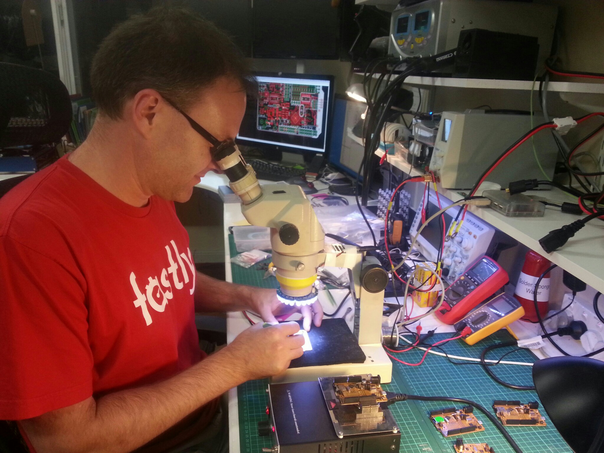
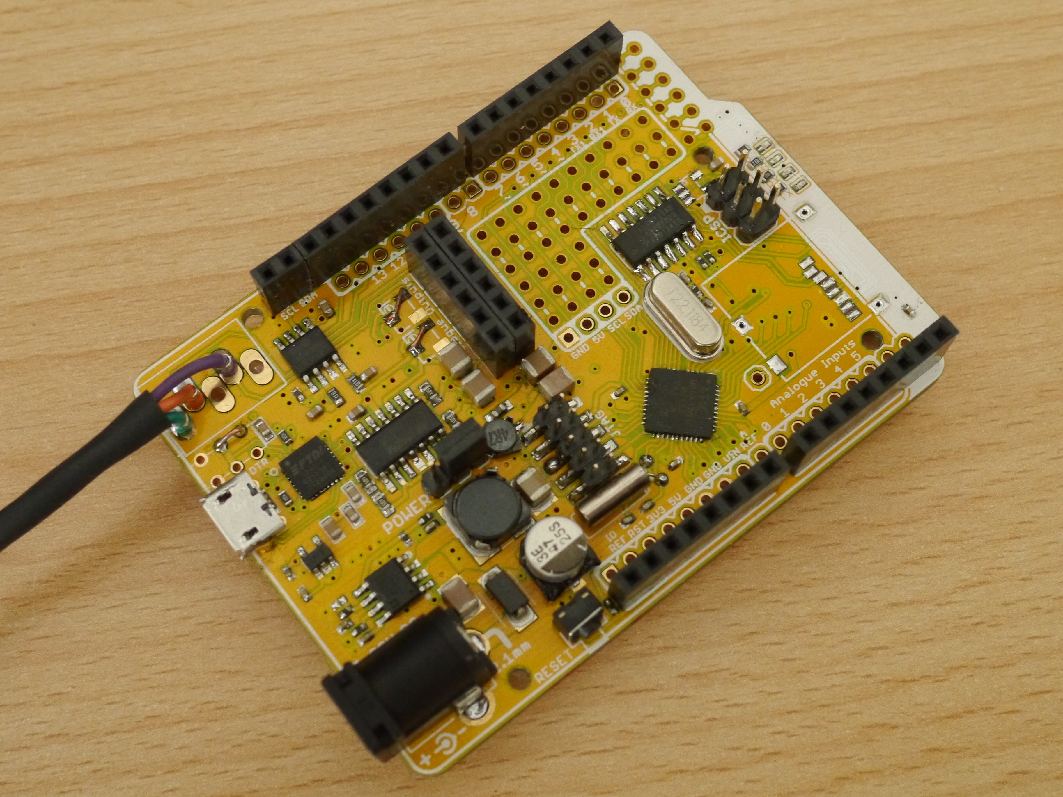
Well I’ve had my Goldilocks Analogue on my desk now for a few nights, and I’m very impressed that it seems to generally meet the specification that was intended.
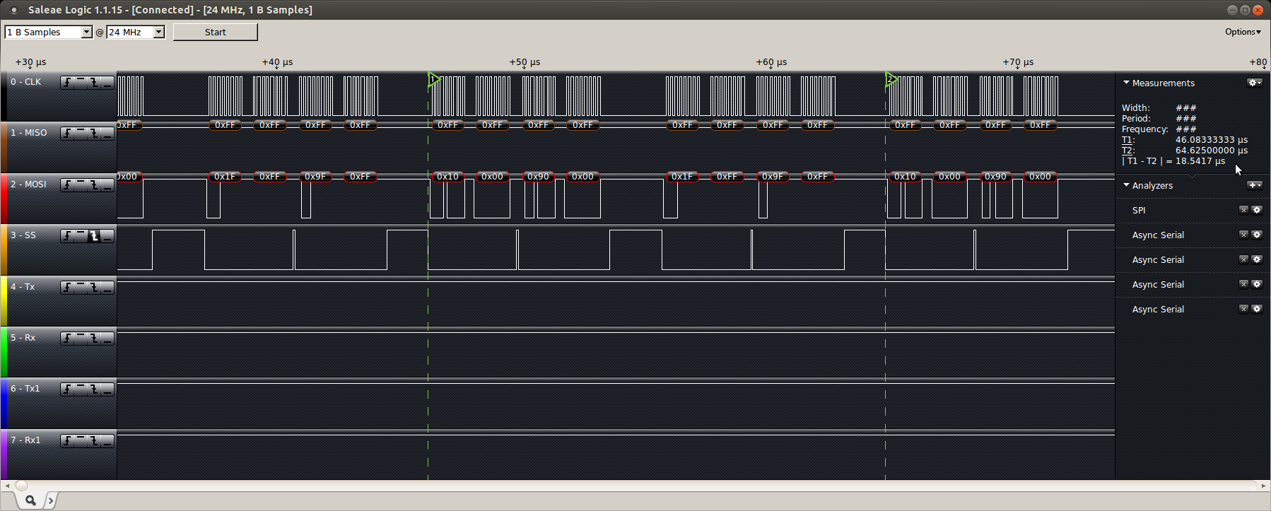
The code for setting the DAC levels is currently only optimised for setting two values at a time. Specifically, it is not a streaming function. Never-the-less, it is possible to achieve the stated goal for both DAC channels. The actual number achieved is 108 kSamples/second, shown below, or 18.8us to transmit 2 samples on 2 channels.
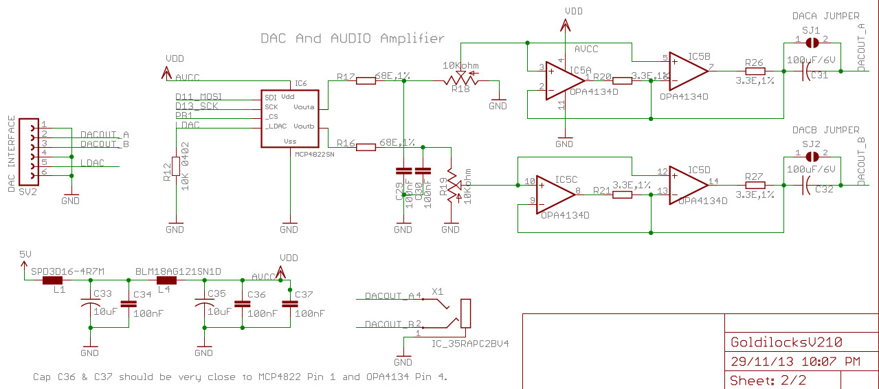
I’ve been testing the Goldilocks Analogue DAC stage and found (what I should have known) that I needed an output buffer op-amp able to do negative rail (0V) input and output to support the MCP4822 0v to 4.095V ranging DAC, so I’m going to order some soon.
Unfortunately the OPA4350 (rail to rail high current), at over $10 each, is nearly as expensive as the audiophile OPA4132 I specified previously.
There seems to be a pin compatible alternative, the TS924A, which is about $2 each, but several orders of magnitude worse in performance.
For Example: OPA4350 vs TS924A
Gain Bandwidth Product: 38MHz vs 4MHz
Slew Rate: 22V/μs vs 1.3V/μs
Total Harmonic Distortion: 0.0006% vs 0.005%
Is it worth the difference, when working with a 12 bit DAC in the presence of mV of power supply noise? I’ll revisit this with the next design notes.
How about 5V?
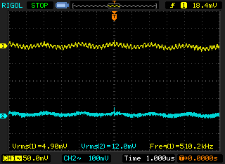
To build an effective DAC I’ve learned that we need to have an effective quiet 5V power supply, with as little noise as possible. To put this into context, the 12 bit MCP4822 generates a 1mV per level difference. I noticed there is quite a few mV of noise on the 5V supply of the Goldilocks Analogue. Not what I was hoping to see, so I’ve gone back to see how that compares with predecessors.
All measurements are taken with a 100MHz Rigol DS1102E, with 150MHz probes grounded onto the USB socket of each board respectively. The probes are directly on the regulator output capacitor, which should be the quietest point on the board, and then directly off Vcc on the MCU for the DIL boards, or a nearby test point for the SMD boards.
First stop is a reference design Arduino Uno R2 board. As a starting point the Uno shows 16mV on the power supply, and 35mV on the MCU. Let’s see how some other boards compare.

Arduino Uno
The Freetronics Eleven board also uses a linear regulator, similar (if not identical to) the Arduino Uno. However the capacitor arrangement must be somewhat more effective because the noise present on the output capacitor is less than 6mV. This is significantly better than on the Arduino Uno, and even measured against the Vcc pin the supply noise remains significantly lower than the Uno.
This Freetronics Eleven board was running at 22.1184MHz rather than the standard Arduino speed, but that doesn’t seem to affect the result.
Freetronics Eleven
Next up is the Seeed Studio ADK boards is an ATmega2560 board running at 16MHz, which also uses a linear regulator. The ADK board exhibits the same quiet supply found in the Freetronics Eleven, and has very similar characteristics on the Vcc test point as well.
Seeed Studio ADK
The Goldilocks v1.1 resulting from the Pozible project is my true point of reference. I hope to be able to do slightly better than this board, by better layout of the same SMPS circuit that is used across all of the Freetronics range of products.
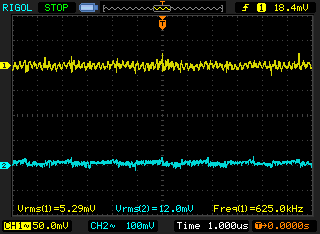
In measurement, the Goldilocks v1.1 sets a very high standard to surpass. Even though there is a 500kHz SMPS running in the supply, the Vcc supply capacitor shows very low noise of only 5.29mV, and the Vcc noise on the test point is only 12.0mV.
Goldilocks V1.1
The Goldilocks Analogue Prototype 1 uses the same SMPS circuit present across the entire range of Freetronics boards, but using an optimised (for this application) layout. Shorter internal tracks should result in slightly faster smoothing, and better regulation, although the effect at normal currents would be minimal.
In comparison with the Goldilocks v1.1, there seems to be slightly less noise at the supply capacitor with less than 5mV showing, although this effect is marginal. The noise on the Vcc line seems to be similar.
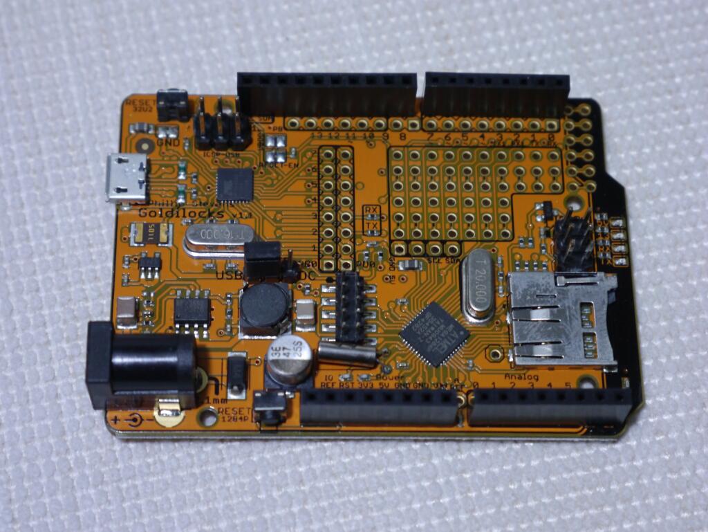
Goldilocks Analogue Prototype 1
SMPS
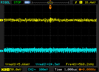
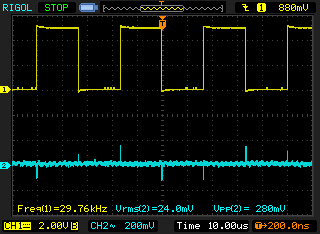
Having looked at the power supplies at rest, and built a baseline of what to expect, here are some screenshots of the Goldilocks SMPS under load. Port D is being switched from 0x00 to 0xFF at 30kHz. The first screenshot shows one of the Port D pins on channel 1, and the Vcc (5V) line at the supply capacitor on channel 2. Note that there is 24mV of noise on the Vcc supply capacitor, even without drawing much current.
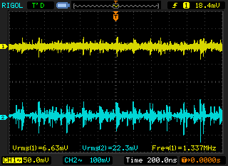
This second screenshot shows the same set up, but with 8 LEDs being driven off the Port D. Channel 2 shows the variation in supply capacitor Vcc under the increased load.
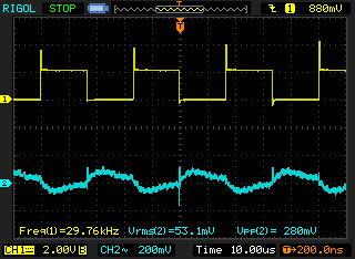
So the big question is whether the new layout of the SMPS has achieved anything. Well, based on this simple test, it would seem to have generated a fairly significant improvement.
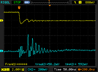
The below two screenshots shows the trailing edge of the 8 LED power load being switched off. Note that on the supply Vcc there is some oscillation and instability as the SMPS recovers from the load reduction.
This first screenshot shows the Goldilocks V1.1 situation, with a ripple of 832mV peak to peak.

With the Goldilocks Analogue, the peak to peak ripple is reduced to under 600mV, which is a 25% improvement in this situation.
Sine Waves
I’m using my new Red Pitaya to analyse the output of the Goldilocks Analogue output state, with a 43.066Hz Sine wave (1024 samples played out at 44.1kHz) as the input to the DAC.
MCP4822 DAC
This shows the sine wave generated at the output of the low pass filter (23kHz -3dB single pole design). This is almost exactly as we would like to see.
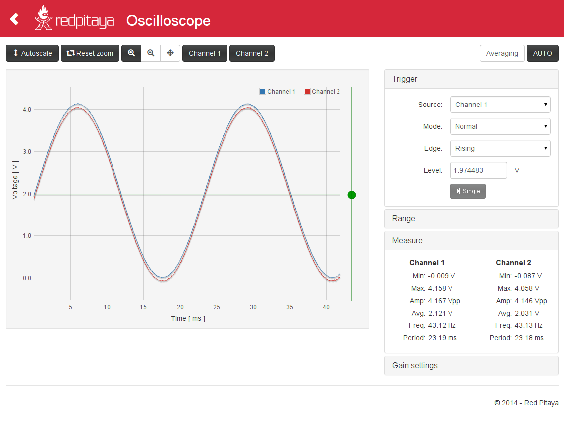
Looking at the lower segment of the sine wave below and the image above, it is almost perfect to 0V and to 4.096V peak to peak.

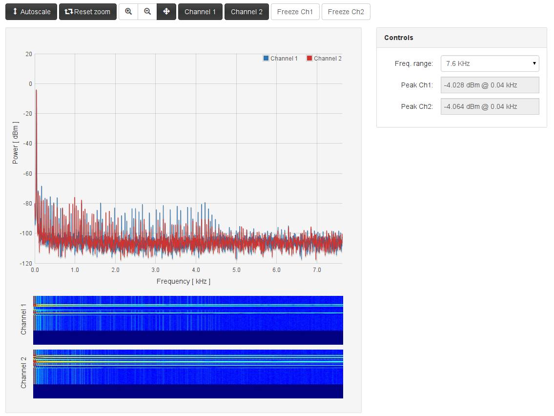
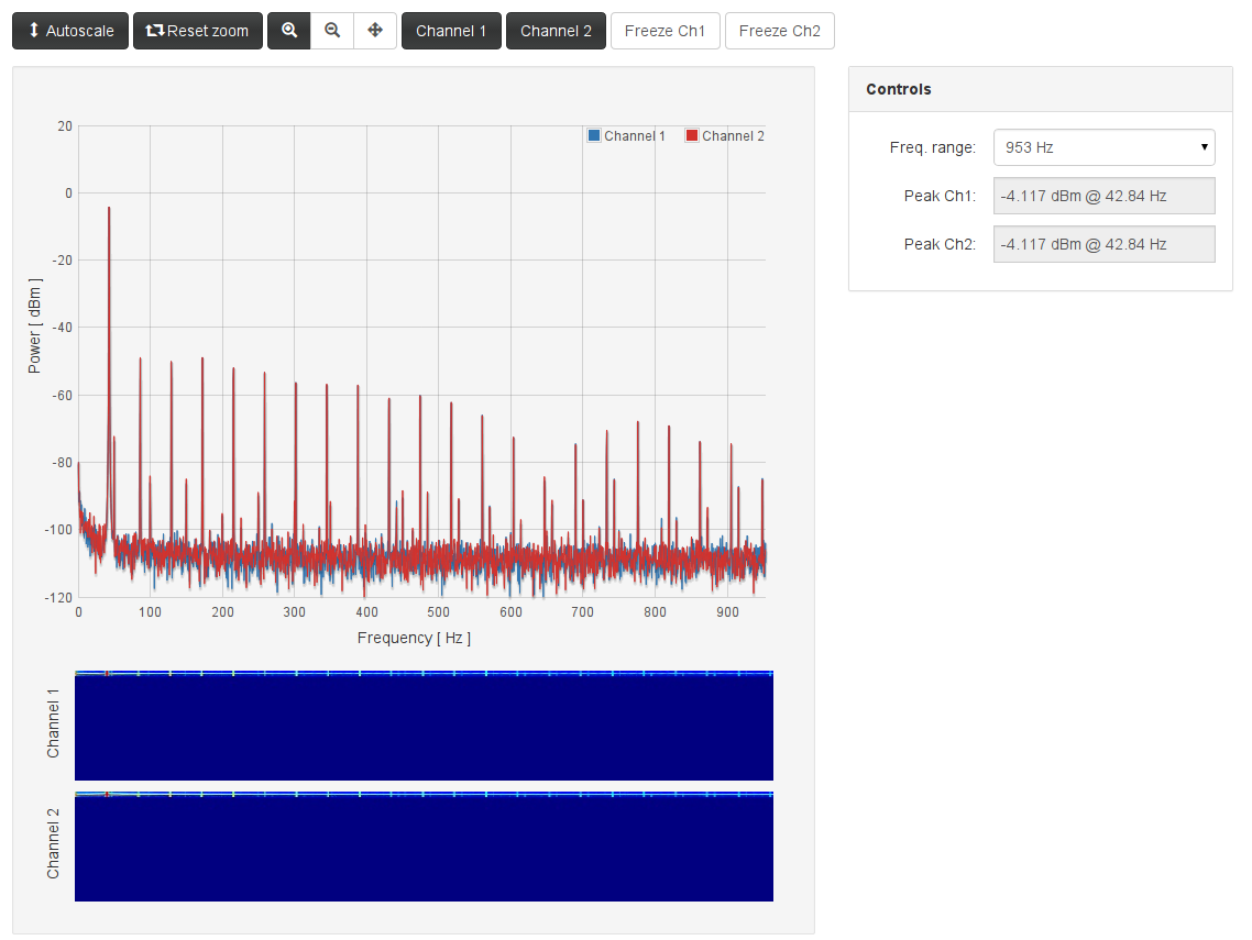
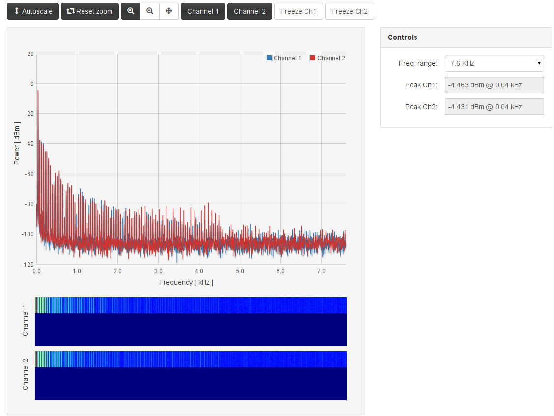
Looking at this sine wave on the spectrum analyser across the band up to 7.6kHz, we can see the noise floor is 70dB down from the signal exiting the DAC. It seems the DAC performs as advertised.
Looking across the band to 61kHz, we can see the peak at -70dbm from the 44.1kHz sampling noise. Unfortunately, the single pole filter doesn’t do much to suppress this noise source.

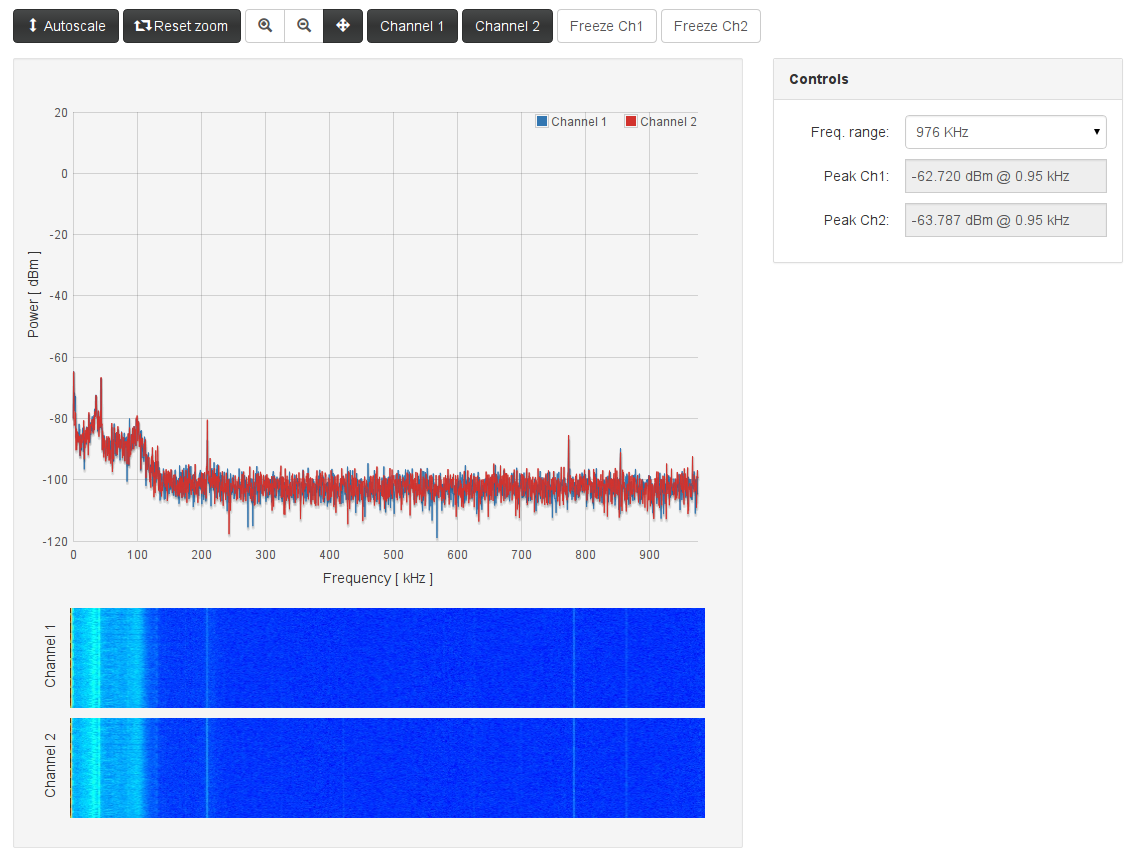
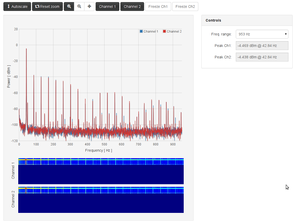
To get an idea of whether the 23kHz filter is working as expected, we need to look out to the 976kHz band. The next two images contract the signal before and after the Filter.
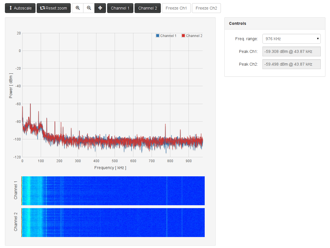
The lower image shows that noise peaks out to 200kHz have been properly suppressed, so the filter is working but it is too slow to hit the 41kHz noise.
Op Amps
The Op Amp selection was a mistake. Rather than thinking about the application correctly, I simply sought out the best “musical” Op Amp. The audiophile OPA4132 is absolutely not the right tool for this job. And these images show why.
Driving into a 1kOhm resistance, the output of the OPA4132 is shaved off as the op amp output amplifier saturates as it approaches the 0V rail (or Ground rail). The top of the waveform is OK, as we are still 1V from the Vcc rail. Under higher loading, such as headphones at 32Ohm, the signal is worse, much worse.

Looking at this (initially as an open circuit) view and then with the 1kOhm loading imposed, we can see the difficulty the op amp has with the signal.
The noise peaks (created by the flattening of the sine wave) are at least 10dB greater under a small load. As the load increases the situation gets worse.

To fix this issue, I will need to use a rail to rail high current op amp, and also make sure that I create a small negative rail (-o.23V using a LM7705) to allow the op amp to reach 0V effectively.
Amongst the Burr Brown range the best alternative seems to be the OPA2353, which can support almost 40mA of current, and can effectively drive 75Ohm loads. Unfortunately the OPA2353 (rail to rail high current) costs about $6 each,
There seems to be a pin compatible alternative, the TS922A, which is about $2 each, but several orders of magnitude worse in performance. However, it can supply 80mA and effectively drive 32Ohm headphones.
For Example: OPA2353 vs TS922A
Gain Bandwidth Product: 44MHz vs 4MHz
Slew Rate: 22V/μs vs 1.3V/μs
Total Harmonic Distortion: 0.0006% vs 0.005%
Errata
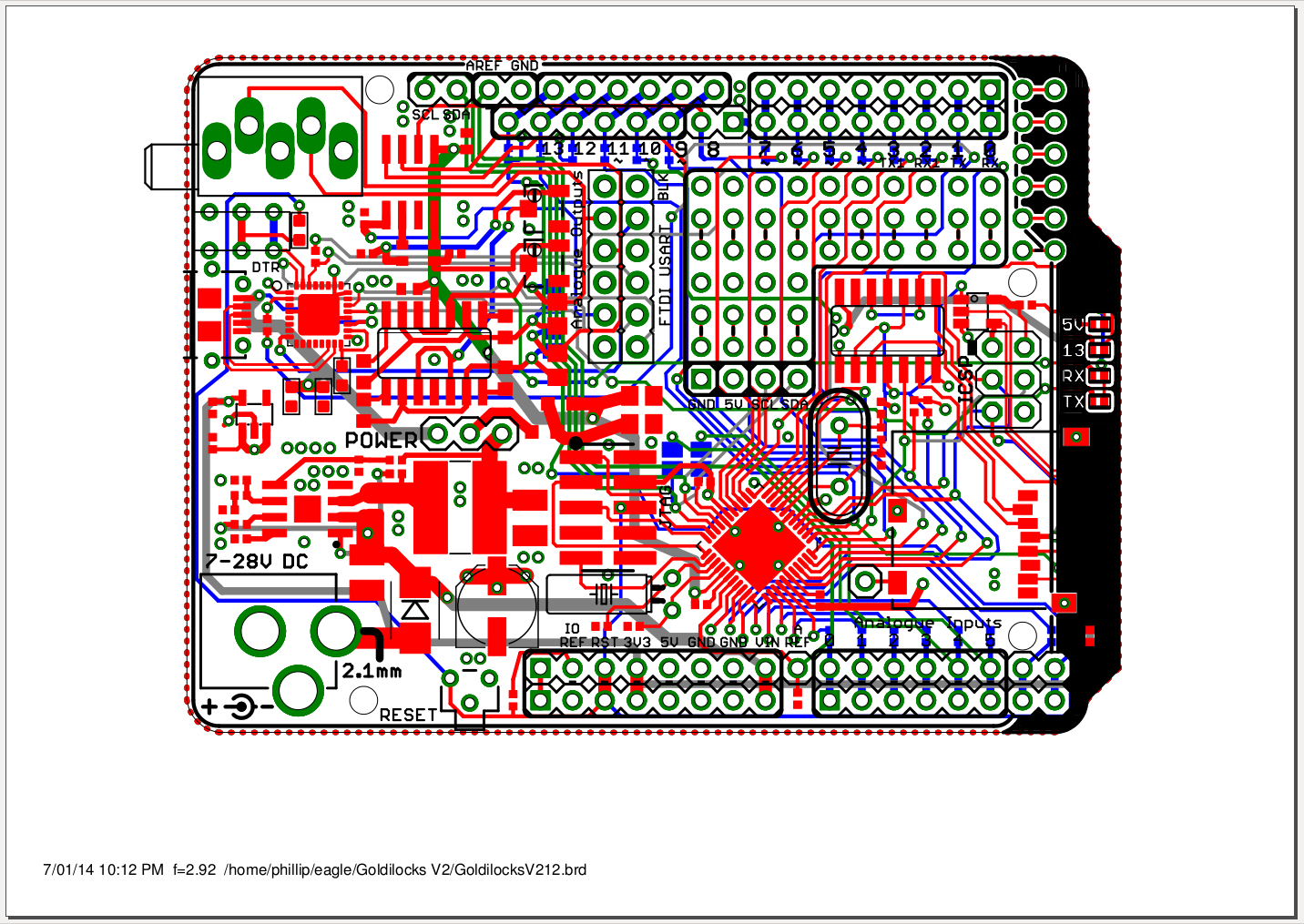
Reset button can be moved closer to the edge.
AVcc supply capacitors are too close together, and need to have bigger pads.
Use the DAC out header spare pin to pin-out the AVcc, for testing or use on prototyping area.
AVcc inductor is not correct footprint (device much larger).
AVcc ferrite bead is not correct footprint (device much smaller).
Remove analogue potentiometers, unnecessary as DAC is extraordinarily accurate.
Put pin-out on DC output, and headphone socket on AC output 100uF capacitors.
Replace Analogue Op Am with LM7705 and TS922A. This generates 0V to 4.096V required to properly buffer the MCP4822 DAC. LM7705 can’t sustain 80mA, but for small DC signals (up to 20mA) we will have accurate buffering of the DAC, and for headphones, it is an analogue signal anyway.
Replace uSD Op Amps with TXB0104, more suitable for the purpose.
These errata have been addressed in the new Goldilocks Analogue design and I have described the changes and additions.