
Just over 6 months since the third iteration of the Goldilocks Analogue Prototyping was started, and now I’ve finished the design for a forth iteration. The Goldilocks Analogue Prototype 4 design is now finished, and I’m working out what the final bill of materials will cost to assemble into a final outcome. Testing for the Prototype 4 has begun, and everything is working as expected.
The third prototype was completely successful, and produced the improvements I was looking for. The use of the MSPI Mode on USART1 means that two SPI interfaces can be run in parallel, allowing the DAC to hold its tight timing requirements while slower SD card transactions take place (for example). This was proven through the implementation of a direct digital synthesiser, controlled by a SPI controlled touch screen.

Goldilocks Analogue – Prototype 3
Revision for Prototype 4
The Prototype 3 was supposed to be the final version, and it achieved everything that I set out in the original design specifications. But, then there was some feature creep.

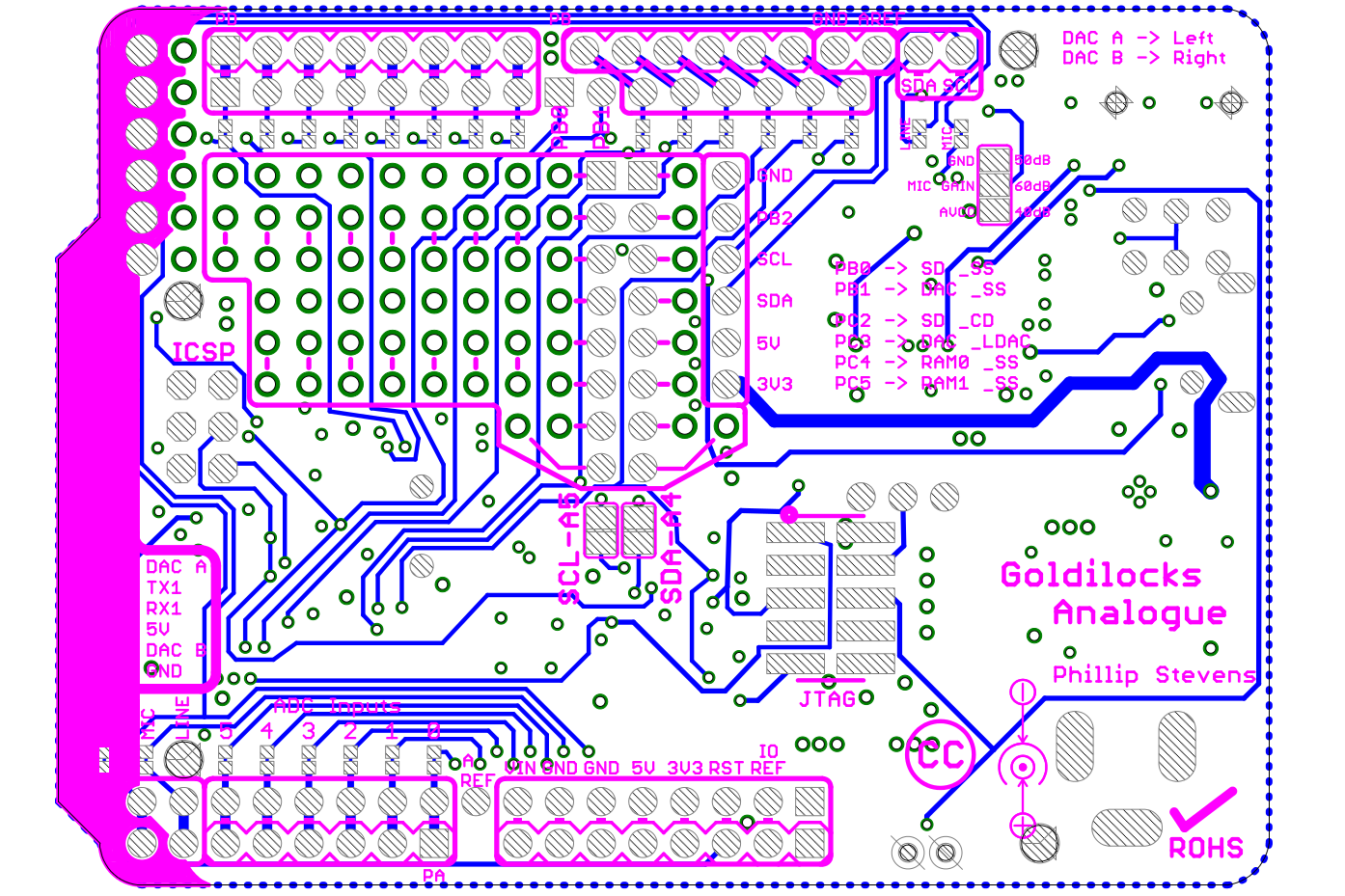
Prototype 4 back from manufacturing
In discussing the TRS 3.5mm audio socket, a better more robust TRRS version was found. The realisation that it would be possible to have a microphone input, without requiring additional board space, led me to experiment with the Adafruit breakout board for the MAX9814 Microphone amplifier, and then to build a very simple Walkie-Talkie demonstration to test the use of audio input (with the integrated ADC), simultaneously with audio output (via the DAC).
Once the use of the MAX9814 was proven, I could implement a reference circuit as an input option. The amplified microphone input is connected to Pin 7 of the Analogue Port A. Conveniently, the MAX9814 delivers the amplified signal at +1.25V with a 2V peak to peak signal. This allows the sample to fall into the range of 0V to 2.56V internal reference voltage for the ATmega ADC, providing the maximum sampling resolution with no further adjustments.
The MAX9814 also includes an integrated microphone biasing circuitry, which is designed to support normal electret microphones.

As an alternative input functionality, the Prototype 4 also allows for LINE level inputs. I have used a voltage divider to reference the input signal to 1.25V DC. Although a 2V peak to peak Line level input will overload the Microphone amplifier, rendering the output signal on PA7 unusable, the LINE input is routed to Pin 6 on Port A will have exactly the right range to sample using the internal ATmega ADC voltage reference.
Both Port A Pin 6 and Pin 7 are outside of the normal Arduino UNO R3 footprint, so the normal functionality of the UNO footprint is not affected by either the two input options. And if desired, the connection can be separated at a solder-jumper on the rear of the board.
The additional space required for the microphone and line level input circuitry has been created by simplifying the negative supply rail for the Op-Amp. The Op-Amp is provided to support DC to 50k sample per second analogue output. To achieve a linear output from 0v to 4.096V the Op-Amp requires a negative supply voltage. In this revision, I have used a single LTC1983 regulated supply device to provide the negative -3V supply rail. The outcome should be equivalent to the Prototype 3 solution, which used 3 devices.
Board Layout
The final board layout has been completed, and the board is now in discussion for manufacturing.
The GoldilocksAnalogueP4Schematic in PDF format.
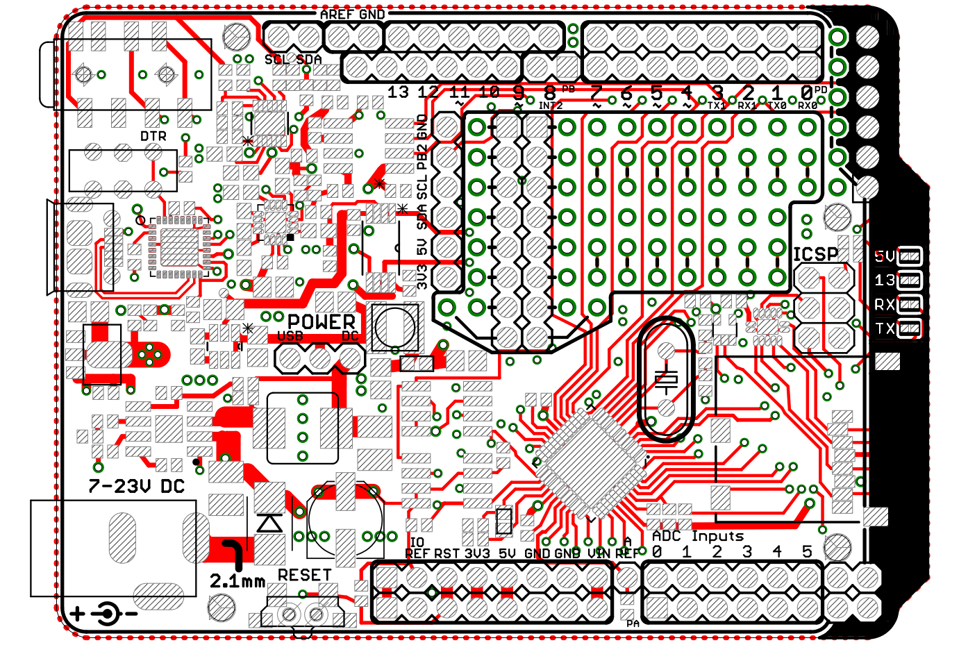
Front of board (All Layers)

This is the front of the board showing all of the layers, and the general layout of the devices. The board layout is pretty busy, but still there is sufficient prototyping capability to take all the port pins off-board, or provide on-board breakouts.


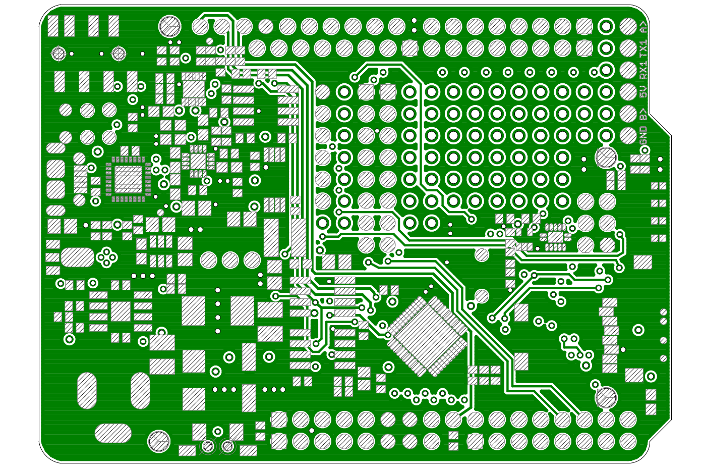
Top Layer
This is the Top Layer, which contains all of the devices. There are no devices on the Bottom Layer.

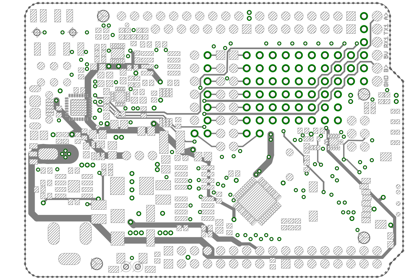
Route 2 (GND) Layer
The Ground Layer on Route 2 is unchanged from previous iterations, and provides a solid platform for low noise analogue circuits.

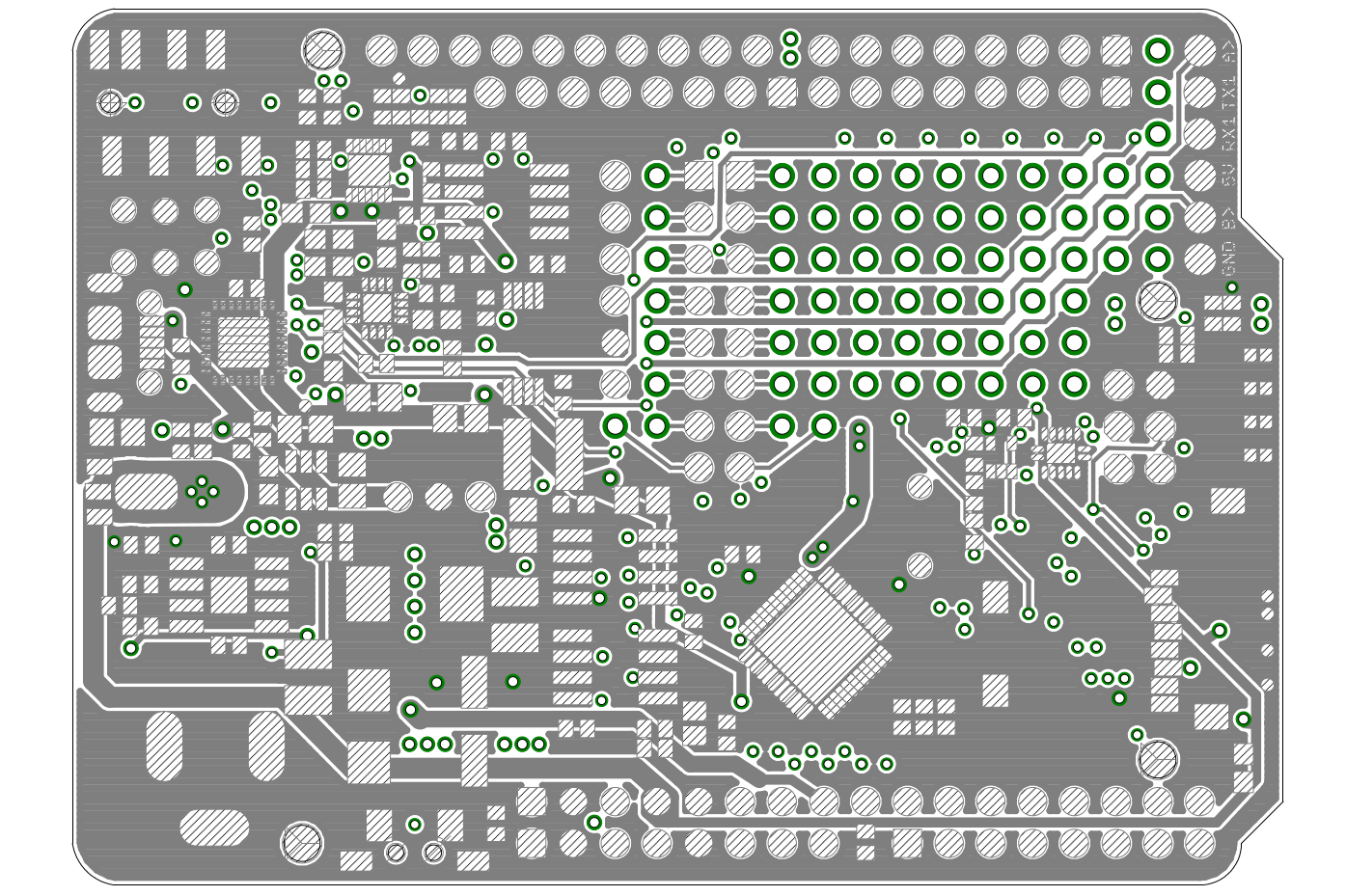
Route 15 (Vcc) Layer
The Route 15 power supply layer contains all of the supply lines, providing 5V regulated, 5V filtered for analogue AVcc, 3.3V regulated, and -3V regulated.
Bottom Layer

All the pin outs are defined on the Bottom Layer. In addition to the items previously mentioned, there are two small locations where the Line and Microphone inputs can be cut, and allow the full functionality of PA6 and PA7 to be recovered.

Pin Mapping
This the map of the ATmega1284p pins to the Arduino physical platform, and their usage on the Goldilocks Analogue
| Arduino UNO R3 |
328p Feature | 328p Pin | 1284p Pin | 1284p Feature | Comment |
| Analog 0 | PC0 | PA0 | |||
| Analog 1 | PC1 | PA1 | |||
| Analog 2 | PC2 | PA2 | |||
| Analog 3 | PC3 | PA3 | |||
| Analog 4 | SDA | PC4 | PA4 | PC1 I2C -> Bridge Pads | |
| Analog 5 | SCL | PC5 | PA5 | PC0 I2C -> Bridge Pads | |
| Reset | Reset | PC6 | RESET | Separate Pin | |
| Digital 0 | RX | PD0 | PDO | RX0 | |
| Digital 1 | TX | PD1 | PD1 | TX0 | |
| Digital 2 | INT0 | PD2 | PD2 | INT0 / RX1 | USART1 |
| Digital 3 | INT1 / PWM2 | PD3 | PD3 | INT1 / TX1 | USART1 -> MCP4822 SPI MOSI |
| Digital 4 | PD4 | PD4 | PWM1 / XCK1 | 16bit PWM -> MCP4822 SPI SCK |
|
| Digital 5 | PWM0 | PD5 | PD5 | PWM1 | 16bit PWM |
| Digital 6 | PWM0 | PD6 | PD6 | PWM2 | |
| Digital 7 | PD7 | PD7 | PWM2 | ||
| Digital 8 | PB0 | PB2 | INT2 | <- _INT/SQW DS3231 | |
| Digital 9 | PWM1 | PB1 | PB3 | PWM0 | |
| Digital 10 | _SS / PWM1 | PB2 | PB4 | _SS / PWM0 | SPI |
| Digital 11 | MOSI / PWM2 | PB3 | PB5 | MOSI | SPI |
| Digital 12 | MISO | PB4 | PB6 | MISO | SPI |
| Digital 13 | SCK | PB5 | PB7 | SCK | SPI |
| (Digital 14 | PB0 | T0 | -> SDCard SPI _SS | ||
| (Digital 15) | PB1 | T1 | -> MCP4822 SPI _SS | ||
| SCL | PC0 | SCL | I2C – Separate | ||
| SDA | PC1 | SDA | I2C – Separate | ||
| PC2 | TCK JTAG | <- _CARD_DETECT for uSD Card |
|||
| PC3 | TMS JTAG | -> MCP4822 _LDAC | |||
| PC4 | TDO JTAG | -> SRAM SPI _SS | |||
| PC5 | TDI JTAG | -> EEPROM SPI _SS | |||
| PC6 | TOSC1 | <- 32768Hz Crystal | |||
| PC7 | TOSC2 | -> 32768Hz Crystal | |||
| XTAL1 | PB6 | ||||
| XTAL2 | PB7 | ||||
| (Analog 6) | PA6 | -> LINE Input | |||
| (Analog 7) | PA7 | -> MIC Input |
